Vertex Standard VX-2200 Series Service Manual
Vhf fm transceiver
Hide thumbs
Also See for VX-2200 Series:
- Service manual (84 pages) ,
- Operating manual (33 pages) ,
- Operating manua (21 pages)
Table of Contents
Advertisement
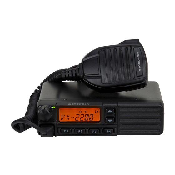
VHF FM Transceiver
VX-2100 Series
VX-2200 Series
Service Manual
©
2008 VERTEX STANDARD CO., LTD.
VX-2100 Series
Introduction
This manual provides the technical information necessary for servicing the VX-2100/-2200 Series Mobile Transceiver.
Servicing this equipment requires expertise in handing surface-mount chip components. Attempts by non-qualified
persons to service this equipment may result in permanent damage not covered by the warranty, and may be illegal
in some countries.
Two PCB layout diagrams are provided for each double-sided board in this transceiver. Each side of the board is
referred to by the type of the majority of components installed on that side ("Side A" or "Side B"). In most cases one
side has only chip components (surface-mount devices), and the other has either a mixture of both chip and leaded
components (trimmers, coils, electrolytic capacitors, ICs, etc.), or leaded components only.
As described in the pages to follow, the advanced microprocessor design of the VX-2100/-2200 allows a complete
alignment of this transceiver to be performed without opening the case of the radio; all adjustments can be performed
from the personal computer, using with the Vertex Standard VPL-1 Programming Cable and CE82 Software.
While we believe the information in this manual to be correct, Vertex Standard assumes no liability for damage that
may occur as a result of typographical or other errors that may be present. Your cooperation in pointing out any
inconsistencies in the technical information would be appreciated.
This transceiver was assembled using Pb (lead) free solder, based on the RoHS specification.
Only lead-free solder (Alloy Composition: Sn-3.0Ag-0.5Cu) should be used for repairs performed on this ap-
paratus. The solder stated above utilizes the alloy composition required for compliance with the lead-free
specification, and any solder with the above alloy composition may be used.
Specifications ........................................................... A-1
DSUB 15-pin Accessory Connector ...................... B-1
Block Diagram ......................................................... D-1
Circuit Description .................................................. E-1
Alignment ................................................................. F-1
Installation of Option ............................................ G-1
EC061N90D
Important Note
Contents
Board Units (Schematics, Layouts & Parts)
MAIN Unit .......................................................... H-1
FRONT-A Unit ( VX-2100 ) ................................... I-1
FRONT-B Unit ( VX-2200 ) ................................... J-1
Optional Units (Schematics, Layouts & Parts)
FVP-25 Encryption/DTMF Pager Unit ............. K-1
VERTEX STANDARD CO., LTD.
4-8-8 Nakameguro, Meguro-Ku, Tokyo 153-8644, Japan
VERTEX STANDARD
US Headquarters
10900 Walker Street, Cypress, CA 90630, U.S.A.
YAESU EUROPE B.V.
P.O. Box 75525, 1118 ZN Schiphol, The Netherlands
YAESU UK LTD.
Unit 12, Sun Valley Business Park, Winnall Close
Winchester, Hampshire, SO23 0LB, U.K.
VERTEX STANDARD HK LTD.
Unit 5, 20/F., Seaview Centre, 139-141 Hoi Bun Road,
Kwun Tong, Kowloon, Hong Kong
VERTEX STANDARD ( AUSTRALIA ) PTY., LTD.
Normanby Business Park, Unit 14/45 Normanby Road
Notting Hill 3168, Victoria, Australia
VX-2200 Series
Advertisement
Table of Contents

Related Manuals for Vertex Standard VX-2200 Series


Summary of Contents for Vertex Standard VX-2200 Series
-
Page 1: Table Of Contents
Vertex Standard VPL-1 Programming Cable and CE82 Software. While we believe the information in this manual to be correct, Vertex Standard assumes no liability for damage that may occur as a result of typographical or other errors that may be present. Your cooperation in pointing out any inconsistencies in the technical information would be appreciated. -
Page 2: Specifications
Specifications (VTX/EXP Version) General Frequency Ranges: 134 -174 MHz Number of Groups: 1 groups (VX-2100 Series) 8 groups (VX-2200 Series) Number of Channels: 8 channels (VX-2100 Series) 128 channels (VX-2200 Series) Power Supply Voltage: 13.6 V ± 15% Channel Spacing: 6.25 / 12.5 / 25 kHz... - Page 3 Specifications (EU Version) General Frequency Ranges: 134 -174 MHz Number of Groups: 1 groups (VX-2100 Series) 8 groups (VX-2200 Series) Number of Channels: 8 channels (VX-2100 Series) 128 channels (VX-2200 Series) Power Supply Voltage: 10.8 - 15.6 V DC Channel Spacing: 12.5 / 20 / 25 kHz...
-
Page 4: Dsub 15-Pin Accessory Connector
DSUB 15-pin Accessory Connector Pin 1: AF IN ( A Pin 6: EXT PTT NALOG NPUT External Microphone Input. Nominal input level is 6 Shorting this port to ground causes the transceiver to mV at 600-ohm. be placed in the Transmit mode, while opening the When connect the External Microphone to this port, connection to this port returns the transceiver to the insert a 0.1 µF coupling capacitor between the micro-... -
Page 5: Exploded View & Miscellaneous Parts
Exploded View & Miscellaneous Parts VX-2100 FRONT PANEL FRONT-A-UNIT RA0790200 TOP CASE RA0787600 RA080360A LIGHT GUIDE (x3 pcs) RA0841400 RUBBER PACKING BLIND SHEET RA078750A HOLDER RA0800600 T9318283 SPONGE RUBBER RA0786500 (Lot 1-4) WIRE ASSY (RED) RA0845300 (Lot 5-) RUBBER KNOB RA0832200 RA0790300 SHEET... - Page 6 Exploded View & Miscellaneous Parts Note:...
-
Page 7: Block Diagram
Block Diagram... - Page 8 Block Diagram Note:...
-
Page 9: Circuit Description
Circuit Description 1. Circuit Configuration by Frequency 2-4. Audio amplifier Detected signal from Q1036 (NJM2591V) is inputted to The receiver is a double-conversion superheterodyne with Q1042 (LM2902PW) and is output through the band pass a first intermediate frequency (IF) of 67.65 MHz and a filter inside Q1042 (LM2902PW). -
Page 10: Transmitter System
Circuit Description 3. Transmitter System 3-4-1. VCO While the radio is receiving, the RX oscillator Q1029 3-1. Mic Amplifier (2SK508) in the VCO generates a programmed frequency There are two micrphone inputs, J1004 (front) and J1006 between 201.65 and 241.65 MHz as 1st local signal. While (D-Sub). -
Page 11: Alignment
Regulated DC Power Supply (standard 13.6V DC, 15A) ponent replacement and service should be performed only Frequency Counter: ±0.2 ppm accuracy at 200 MHz by an authorized Vertex Standard representative, or the AF Signal Generator warranty policy may be voided. -
Page 12: Test Setup
Alignment Test Setup Basic Alignment Mode Setup the test equipment as shown for transceiver align- The Basic Alignment mode allows you to align the entire ment, apply 13.6V DC power to the transceiver. Refer to radio. The value of each parameter can be changed to the the drawings above for Alignment Points. - Page 13 Alignment Unit During alignment, the values of dBµV or µV (EMF or PD) can be selected or dBm. 1. RX VCO Tune Voltage (RX VCO) This parameter is to align the “Tune Voltage” of RX VCO. This alignment will be done automatically between the radio and PC.
- Page 14 Alignment 3. PLL Reference Frequency (Frequency) This parameter is to align the reference frequency for PLL. The “TX VCO Tune Voltage” alignment must be done before this alignment is going to start. 1. Press the “Start” button to start the alignment then the radio will transmit on the center frequency.
- Page 15 Alignment RSSI SQL Full Scale <Wide> (S Full Scale W) The Alignment for the RSSI Full Scale level at Wide (5k/ 4k). Noise SQL Tight <Narrow> (TI NSQ N) The Alignment for the Noise SQL Tight level at Narrow (2.5k). Noise SQL Threshold <...
-
Page 16: Maximum/Sub Audio/Sequential Tone Deviations
Alignment 7. Maximum Deviation <Wide> / <Narrow> This parameter is to align the Maximum Deviation (Wide/Narrow). The “TX VCO Tune Voltage” must be done before this alignment is started. 1. Press the “Start” button to start the alignment. 2. Set the value to get desired deviation (Wide: 4.2kHz, Narrow: 2.1kHz) on the deviation meter by changing the slide bar on your PC. - Page 17 Alignment CH (Channel-by-Channel) Fine Alignment Mode The CH Fine Alignment Mode allows you to align the radio separately for every operating channel. The value of each parameter can be changed to the desired position using the “ ” / “ ” and up/down arrow keys, direct number input, and by dragging the PC mouse.
-
Page 18: Installation Of Option
Installation of Option FVP-25/FVP-35/FVP-36 The FVP-25 is an Encryption/DTMF Pageing Unit which 1. Disconnect the DC power cable. permits secure voice communications with station within 2. Referring to Figure 1, remove the 8 screws affixing the your network, while preventing others from listening us- Top Cover, then remove the top cover. -
Page 19: Main Unit
MAIN Unit (Lot. 1~4) 67.65MHz RX:1.3V RX:7.4V -121.5dBm -103.0dBm 67.65MHz -81.5dBm RX:8.0V TX:0V TX:0V -123.8dBm (C1046 removed) -111.0dBm (C1146 removed) -108.5dBm -102.5dBm (C1230 removed) TX:0V RX:7.5V RX:2.0V -110.0dBm (C1198 removed) TX:0V Circuit Diagram TX:0V RX:2.0V TX:0V RX:4.3V TX:0V RX:1.4V -103.0dBm TX:0V -108.5dBm (C1093 removed) 8.1V... - Page 20 MAIN Unit (Lot. 1~4) Note...
- Page 21 MAIN Unit (Lot. 1~4) Parts Layout (Side A) UA78M08CKTPR (Lot.1-4) (Q1006) SN74LV4053APWR (Q1004, 1005) LM2902PWR (Q1040, 1042, 1043, 1045, 1046, 1048,1049) MTM231230L (BL) (Q 1008, 1011, 1012) 2SK397300L (Q1050, 1055, 1060, 1063, 1070) S-AV32 (Q1009) UMG2N (Q1013) M62364FP RT1N441U (N3) 3SK293 (UF) BH2220FVM TAR5S35(3V5)
- Page 22 MAIN Unit (Lot. 1~4) Parts Layout (Side B) DAN222 (N) (D1020, 1035, 1039) MC2850 (A7) (D1021, 1027, 1041 1046, 1047, 1048 1053, 1054) 2SK508 (K52) (Q1029) 2SK880GR (XG) (Q1037) 2SC4617 (BR) (Q1018, 1019, 1020, TDA1519CTH SN74LV4066APWR ADF4111BRUZ-RL7 LM2902PWR DTA124EE (15) RT1N140U RT1N441U (N3) S-80835CNMC...
- Page 23 MAIN Unit (Lot. 5~8) Circuit Diagram...
- Page 24 MAIN Unit (Lot. 5~8) Note...
-
Page 25: Main Unit (Lot. 5~8) Parts Layout
MAIN Unit (Lot. 5~8) Parts Layout (Side A) NJM7808DL1A (Q1006) SN74LV4053APWR (Q1004, 1005) NJM12902V (Q1040, 1042, 1043, 1045, 1046, 1048,1049) LM2902PWR (Lot. 7~) (Q1045) MTM231230L (BL) (Q 1008, 1011, 1012) 2SK397300L (Q1050, 1055, 1060, 1063, 1070) S-AV32 (Q1009) UMG2N (Q1013) M62364FP RT1N441U (N3) 3SK293 (UF) - Page 26 MAIN Unit (Lot. 5~8) Parts Layout (Side B) DAN222 (N) (D1020, 1035, 1039) MC2850 (A7) (D1021, 1027, 1041 1046, 1047, 1048 1053, 1054) 2SK508 (K52) (Q1029) 2SK880GR (XG) (Q1037) 2SC4617 (BR) (Q1018, 1019, 1020, TDA1519CTH SN74LV4066APWR ADF4111BRUZ-RL7 NJM12902V DTA124EE (15) RT1N140U RT1N441U (N3) DTC143EE (23) (Lot.
- Page 27 MAIN Unit (Lot. 9~17) Circuit Diagram...
- Page 28 MAIN Unit (Lot. 9~17) Note H-10...
- Page 29 MAIN Unit (Lot. 9~17) Parts Layout (Side A) NJM7808DL1A (Q1006) SN74LV4053APWR (Q1004, 1005) NJM12902V (Q1040, 1042, 1043, 1045, 1046, 1048,1049) MTM231230L (BL) (Q 1008, 1011, 1012) 2SK397300L (Q1050, 1055, 1060, 1063, 1070) S-AV32 (50 W) S-AV33 (25 W) (Q1009) UMG2N (Q1013) M62364FP RT1N441U (N3)
- Page 30 MAIN Unit (Lot. 9~17) Parts Layout (Side B) DAN222 (N) (D1020, 1035, 1039) MC2850 (A7) (D1021, 1027, 1041 1046, 1047, 1048 1053, 1054) 2SK508 (K52) (Q1029) 2SK880GR (XG) (Q1037) 2SC4617 (BR) (Q1018, 1019, 1020, TDA1519CTH SN74LV4066APWR ADF4111BRUZ-RL7 NJM12902V LC73881M DTA124EE (15) RT1N140U RT1N441U (N3) DTC143EE (23)
- Page 31 MAIN Unit (Lot. 18~20) Circuit Diagram H-13...
- Page 32 MAIN Unit (Lot. 18~20) Note H-14...
-
Page 33: Main Unit (Lot. 18~20) Parts Layout
MAIN Unit (Lot. 18~20) Parts Layout (Side A) NJM7808DL1A (Q1006) SN74LV4053APWR (Q1004, 1005) NJM12902V (Q1040, 1042, 1043, 1045, 1046, 1048,1049) MTM231230L (BL) (Q 1008, 1011, 1012) 2SK397300L (Q1050, 1055, 1060, 1063, 1070) S-AV32 (50 W) S-AV33 (25 W) (Q1009) UMG2N (Q1013) M62364FP RT1N441U (N3) - Page 34 MAIN Unit (Lot. 18~20) Parts Layout (Side B) DAN222 (N) (D1020, 1035, 1039) MC2850 (A7) (D1021, 1027, 1041 1046, 1047, 1048 1053, 1054) 2SK508 (K52) (Q1029) 2SK880GR (XG) (Q1037) 2SC4617 (BR) (Q1018, 1019, 1020, TDA1519CTH SN74LV4066APWR ADF4111BRUZ-RL7 NJM12902V LC73881M DTA124EE (15) RT1N140U RT1N441U (N3) DTC143EE (23)
-
Page 35: Main Unit (Lot. 21~) Circuit Diagram
MAIN Unit (Lot. 21~) Circuit Diagram H-17... - Page 36 MAIN Unit (Lot. 21~) Note H-18...
- Page 37 MAIN Unit (Lot. 21~) Parts Layout (Side A) NJM7808DL1A (Q1006) SN74LV4053APWR (Q1004, 1005) NJM12902V (Q1040, 1042, 1043, 1045, 1046, 1048,1049) MTM231230L (BL) (Q 1008, 1011, 1012) 2SK397300L (Q1050, 1055, 1060, 1063, 1070) S-AV32 (50 W) S-AV33 (25 W) (Q1009) UMG2N (Q1013) M62364FP RT1N441U (N3) (Lot.
- Page 38 MAIN Unit (Lot. 21~) Parts Layout (Side B) DAN222 (N) (D1020, 1035, 1039) MC2850 (A7) (Lot. 1~22) DAN217U (A7) (Lot. 23~) (D1021, 1027, 1041 1046, 1047, 1048 1053, 1054) 2SK508 (K52) (Q1029) 2SK880GR (XG) (Q1037) 2SC4617 (BR) (Q1018, 1019, 1020, TDA1519CTH SN74LV4066APWR ADF4111BRUZ-RL7...
-
Page 39: Main Unit
MAIN Unit Parts List DESCRIPTION VALUE TOL. MFR'S DESIG VXSTD P/N VERS. LOT SIDE LAY ADR PCB with Components CS1873001 VTX 50 W CS1873002 VTX 25 W CS1873003 EU 25 W CS1873004 EXP 50 W CS1873005 EXP 25 W Printed Circuit Board FR012250E FR012250G FR012250I... -
Page 40: Parts List
MAIN Unit Parts List DESCRIPTION VALUE TOL. MFR'S DESIG VXSTD P/N VERS. LOT SIDE LAY ADR C 1046 CHIP CAP. 0.001uF GRM155B11H102KA01D K22178809 C 1047 CHIP CAP. 0.001uF GRM155B11H102KA01D K22178809 C 1048 CHIP CAP. 0.001uF GRM155B11H102KA01D K22178809 C 1049 CHIP CAP. 0.1uF GRM21BB11E104KA01L K22140811... - Page 41 MAIN Unit Parts List DESCRIPTION VALUE TOL. MFR'S DESIG VXSTD P/N VERS. LOT SIDE LAY ADR C 1116 CHIP CAP. GRM1552C1H7R0BZ01D K22178294 C 1117 CHIP CAP. 0.0022uF GRM155B11H222KA01D K22178813 C 1118 CHIP CAP. 0.01uF GRM36B103K16PT K22128804 C 1118 CHIP CAP. 0.01uF GRM155B11E103KA01D K22148834...
- Page 42 MAIN Unit Parts List DESCRIPTION VALUE TOL. MFR'S DESIG VXSTD P/N VERS. LOT SIDE LAY ADR C 1192 CHIP CAP. 39pF GRM1552C1H390JZ01D K22178226 C 1193 CHIP CAP. 10pF GRM1552C1H100JZ01D K22178212 C 1195 CHIP CAP. 18pF GRM1552C1H180JZ01D K22178218 C 1196 CHIP CAP. 0.0047uF GRM36B472K25PT K22148830...
- Page 43 MAIN Unit Parts List DESCRIPTION VALUE TOL. MFR'S DESIG VXSTD P/N VERS. LOT SIDE LAY ADR C 1258 CHIP CAP. 12pF GRM1552C1H120JZ01D K22178214 C 1259 CHIP CAP. 180pF GRM36CH181J25PT K22148201 C 1259 CHIP CAP. 180pF GRM1552C1H181JA01D K22179711 C 1260 CHIP CAP. 0.001uF GRM155B11H102KA01D K22178809...
- Page 44 MAIN Unit Parts List DESCRIPTION VALUE TOL. MFR'S DESIG VXSTD P/N VERS. LOT SIDE LAY ADR C 1313 CHIP CAP. 0.01uF GRM36B103K16PT K22128804 C 1313 CHIP CAP. 0.01uF GRM155B11E103KA01D K22148834 C 1314 CHIP CAP. 0.01uF GRM36B103K16PT K22128804 C 1314 CHIP CAP. 0.01uF GRM155B11E103KA01D K22148834...
- Page 45 MAIN Unit Parts List DESCRIPTION VALUE TOL. MFR'S DESIG VXSTD P/N VERS. LOT SIDE LAY ADR D 1028 DIODE 1SV325(TPH3.F) G2070848 D 1029 DIODE 1SV325(TPH3.F) G2070848 D 1030 DIODE 1SV325(TPH3.F) G2070848 D 1031 DIODE 1SV325(TPH3.F) G2070848 D 1032 DIODE 1SV325(TPH3.F) G2070848 D 1033 DIODE...
- Page 46 MAIN Unit Parts List DESCRIPTION VALUE TOL. MFR'S DESIG VXSTD P/N VERS. LOT SIDE LAY ADR L 1016 M.RFC 0.22uH HK1608 R22J-T L1690940 L 1017 M.RFC 0.082uH HK1608 82NJ-T L1690527 L 1017 M.RFC 0.22uH HK1608 R22J-T L1690940 L 1018 M.RFC 0.082uH HK1608 82NJ-T L1690527...
- Page 47 RMC1/16S 472JTH J24189033 R 1005 CHIP RES. 1/16W RMC1/16S 473JTH J24189045 R 1005 CHIP RES. 1/16W RMC1/16S 223JTH J24189041 R 1006 CHIP RES. 470k 1/16W RMC1/16S 474JTH J24189057 R 1007 CHIP RES. RMC1 101JTE J24305101 : Please contact Vertex Standard H-29...
- Page 48 MAIN Unit Parts List DESCRIPTION VALUE TOL. MFR'S DESIG VXSTD P/N VERS. LOT SIDE LAY ADR R 1008 CHIP RES. 470k 1/16W RMC1/16S 474JTH J24189057 R 1009 CHIP RES. 470k 1/16W RMC1/16S 474JTH J24189057 R 1009 CHIP RES. 270k 1/16W RMC1/16S 274JTH J24189054 R 1010...
- Page 49 MAIN Unit Parts List DESCRIPTION VALUE TOL. MFR'S DESIG VXSTD P/N VERS. LOT SIDE LAY ADR R 1057 CHIP RES. 1/16W RMC1/16S 105JTH J24189061 R 1058 CHIP RES. 100k 1/16W RMC1/16S 104JTH J24189049 R 1058 CHIP RES. 1/16W RMC1/16S 473JTH J24189045 R 1058 CHIP RES.
- Page 50 MAIN Unit Parts List DESCRIPTION VALUE TOL. MFR'S DESIG VXSTD P/N VERS. LOT SIDE LAY ADR R 1133 CHIP RES. 1/16W RMC1/16S 823JTH J24189048 R 1135 CHIP RES. 100k 1/16W RMC1/16S 104JTH J24189049 R 1136 CHIP RES. 100k 1/16W RMC1/16S 104JTH J24189049 R 1137 CHIP RES.
- Page 51 MAIN Unit Parts List DESCRIPTION VALUE TOL. MFR'S DESIG VXSTD P/N VERS. LOT SIDE LAY ADR R 1192 CHIP RES. 1/16W RMC1/16S 223JTH J24189041 R 1193 CHIP RES. 1/16W RMC1/16S 103JTH J24189037 R 1194 CHIP RES. 1/16W RMC1/16S 823JTH J24189048 R 1195 CHIP RES.
- Page 52 MAIN Unit Parts List Parts List DESCRIPTION VALUE TOL. MFR'S DESIG VXSTD P/N VERS. LOT SIDE LAY ADR R 1267 CHIP RES. 1/16W RMC1/16S 151JTH J24189015 R 1268 CHIP RES. 1/16W RMC1/16S 223JTH J24189041 R 1269 CHIP RES. 1/16W RMC1/16 000JATP J24185000 R 1270 CHIP RES.
- Page 53 MAIN Unit Parts List DESCRIPTION VALUE TOL. MFR'S DESIG VXSTD P/N VERS. LOT SIDE LAY ADR R 1338 CHIP RES. 1/16W RMC1/16S 473JTH J24189045 R 1339 CHIP RES. 1/16W RMC1/16S 105JTH J24189061 R 1340 CHIP RES. 1/16W RMC1/16S 105JTH J24189061 R 1343 CHIP RES.
- Page 54 MAIN Unit Note H-36...
- Page 55 FRONT-A Unit (VX-2100) Circuit Diagram RX: 4.9V RX: 0V TX: 0V TX: 4.9V 5.0V 13.6V...
- Page 56 FRONT-A Unit (VX-2100) Parts Layout (Side A) RT1N441U (N3) (Lot. 1~22) BRPG1211C DTC144EE (26) (Lot. 23~) (D2001) (Q2011, 2013, 2014, 2015) Parts Layout (Side B) RT1N441U (N3) (Lot. 1~22) CD4094BPWR UA78L05ACPK (F5) DTC144EE (26) (Lot. 23~) (Q2005, 2012) (Q2007) (Q2001, 2002, 2003, 2004, 2006, 2008, 2009, 2010)
-
Page 57: Front-A Unit ( Vx-2100
FRONT-A Unit (VX-2100) Parts List DESCRIPTION VALUE TOL. MFR'S DESIG VXSTD P/N VERS. LOT SIDE LAY ADR PCB with Components CB3472001 Printed Circuit Board FR014510B C 2001 CHIP TA.CAP. 4.7uF TEESVB21E475M8R K78140019 C 2002 CHIP CAP. 0.1uF GRM21BB11E104KA01L K22140811 C 2003 CHIP CAP. - Page 58 FRONT-A Unit (VX-2100) Note...
- Page 59 FRONT-B Unit (VX-2200) Circuit Diagram RX: 4.9V TX: 0V RX: 0V TX: 4.9V DIMMER LEVEL 3: 4.8V 5.0V 5.0V...
- Page 60 FRONT-B Unit (VX-2200) Parts Layout (Side A) BRPG1211C (D3005) (DS3001) Parts Layout (Side B) 2SB1132 (BA) XP1501 (R5) RT1N441U (N3) (Lot. 1~22) CD4094BPWR (Q3001) (Q3002, 3007) DTC144EE (26) (Lot. 23~) (Q3005) (Q3003, 3004) UA78L05ACPK (F5) 2SA1602A (MF) (Lot. 1~15) NJU6533KQ1 (Q3006) ISA1602AM1 (MF) (Lot.
-
Page 61: Front-B Unit ( Vx-2200
FRONT-B Unit (VX-2200) Parts List DESCRIPTION VALUE TOL. MFR'S DESIG VXSTD P/N VERS. LOT SIDE LAY ADR PCB with Components CB3473001 Printed Circuit Board FR014520C C 3001 CHIP TA.CAP. 4.7uF TEESVB21E475M8R K78140019 C 3002 CHIP CAP. 0.1uF GRM21BB11E104KA01L K22140811 C 3003 CHIP CAP. - Page 62 FRONT-B Unit (VX-2200) Note:...
-
Page 63: Fvp-25 Encryption/Dtmf Pager Unit
FVP-25 Encryption/DTMF Pager Unit (Option) Circuit Diagram Parts Layout Side A Side B M64026FP LC73881 DTC144EU (26) (Q1001) (Q1002) (Q1003) - Page 64 FVP-25 Encryption/DTMF Pager Unit (Option) Parts List DESCRIPTION VALUE TOL. MFR'S DESIG VXSTD P/N VERS. LOT SIDE LAY ADR Printed Circuit Board FR005010F C 1001 CHIP CAP. 0.1uF GRM188B11C104KA01D K22124805 C 1002 CHIP CAP. 0.01uF GRM39B103M25PT K22144802 C 1003 CHIP CAP. 10pF GRM1882C1H100JA01D K22174211...
-
Page 65: Fvp-36 Voice Inversion Type Encryption Unit
FVP-36 Voice Inversion Type Encryption Unit (Option) Circuit Diagram Parts Layout M64026FP (Q1001) Side A Side B... - Page 66 FVP-36 Voice Inversion Type Encryption Unit (Option) Parts List DESCRIPTION VALUE TOL. MFR'S DESIG VXSTD P/N VERS. LOT SIDE LAY ADR Printed Circuit Board FR005010F C 1003 CHIP CAP. 10pF GRM1882C1H100JA01D K22174211 C 1004 CHIP CAP. 10pF GRM1882C1H100JA01D K22174211 C 1005 CHIP CAP.
- Page 68 Copyright 2008 VERTEX STANDARD CO., LTD. All rights reserved No portion of this manual may be reproduced without the permission of VERTEX STANDARD CO., LTD.
Need help?
Do you have a question about the VX-2200 Series and is the answer not in the manual?
Questions and answers