Table of Contents
Advertisement
Quick Links
SAFETY PRECAUTION FOR SERVICE MANUAL ............................................................................................................... 2
AC POWER SUPPLY CORD................................................................................................................................................. 2
SPECIFICATIONS ................................................................................................................................................................. 3
LASER BEAM SAFETY PRECAUTIONS .............................................................................................................................. 4
STANDARD NOTES FOR SERVICING................................................................................................................................. 5
OPERATING CONTROLS AND FUNCTIONS ...................................................................................................................... 8
BLOCK DIAGRAMS.............................................................................................................................................................. 10
SCHEMATIC DIAGRAMS..................................................................................................................................................... 11
IC'S PIN VOLTAGE CHART ................................................................................................................................................ 22
WAVEFORMS....................................................................................................................................................................... 25
OVERALL WIRING CONNECTION...................................................................................................................................... 28
WIRING DIAGRAM............................................................................................................................................................... 29
NOTES ON SCHEMATIC DIAGRAM / TYPES OF TRANSISTOR AND LED ...................................................................... 39
TROUBLESHOOTING.......................................................................................................................................................... 40
IC PIN FUNCTION DESCRIPTIONS.................................................................................................................................... 41
Parts marked with "
parts with specified ones for maintaining the safety and performance of the set.
SERVICE MANUAL
CONTENTS
" are important for maintaining the safety of the set. Be sure to replace these
MODEL
• In the interests of user-safety (Required by safety regula-
tions in some countries) the set should be restored to its
original condition and only parts identical to those specified
be used.
This document has been published to be used for
after sales service only.
The contents are subject to change without notice.
1
DV-SL700W
No. S9501DVSL700W
DVD PLAYER
DV-SL700W
Page
Advertisement
Table of Contents

Related Manuals for Sharp DV-SL700W


Summary of Contents for Sharp DV-SL700W
-
Page 1: Table Of Contents
DV-SL700W SERVICE MANUAL No. S9501DVSL700W DVD PLAYER DV-SL700W MODEL • In the interests of user-safety (Required by safety regula- tions in some countries) the set should be restored to its original condition and only parts identical to those specified be used. -
Page 2: Safety Precaution For Service Manual
DV-SL700W SAFETY PRECAUTION FOR SERVICE MANUAL l This product is classified as a CLASS 1 LASER PRODUCT. WARNINGS: The AEL (Accessible Emission Level) of Laser Power Output for this model is specified to be lower than Class 1 Requirements. However, the following precautions must be observed during servicing to protect your eyes against exposure to the Laser beam. -
Page 3: Specifications
DV-SL700W SPECIFICATIONS As part of our policy of continuous improvement, SHARP reserves the right to make design and specification changes for product improvement without prior notice. The performance specification figures indicated are nominal values of production units. There may be some deviations from these values in individual units. -
Page 4: Laser Beam Safety Precautions
DV-SL700W LASER BEAM SAFETY PRECAUTIONS This DVD player uses a pickup that emits a laser beam. Do not look directly at the laser beam coming from the pickup or allow it to strike against Do not look directly at the laser beam coming your skin. -
Page 5: Standard Notes For Servicing
(2) Lift each lead of the flat pack-IC upward one by one, may be apt to keep the soldering bit in contact with the using a sharp pin or wire to which solder will not PWB for extended period of time. However, Since the adhere (iron wire). - Page 6 Hot Air Blower Fig. S-1-3 (2) Lift each lead of the flat pack-IC upward one by one, using a sharp pin or wire to which solder will not adhere (iron wire). When heating the pins, use a fine Fig. S-1-1 tip soldering iron or a hot air desoldering machine.
- Page 7 DV-SL700W (4) Bottom of the flat pack-IC is fixed with glue to the 2. Installation Instructions for Handling CBA; when removing entire flat pack-IC, first apply (1) Using desoldering braid, remove the solder from the Semi-conductors soldering iron to center of the flat pack-IC and heat foil of each pin of the flat pack-IC on the CBA so you up.
-
Page 8: Play
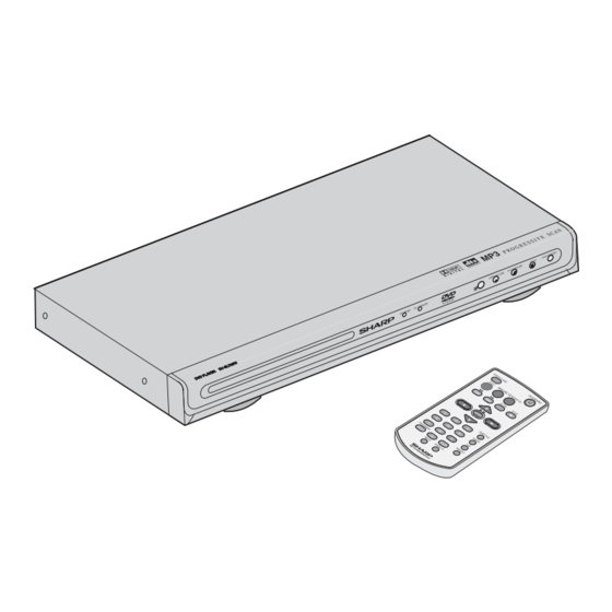
DV-SL700W OPERATING CONTROLS AND FUNCTIONS n Main unit (front panel) 4 5 6 7 Disc Tray Disc Tray OPEN/CLOSE Button STANDBY Indicator Play or Pause Button PLAY/PAUSE Indicator STOP Button Remote Sensor ON/STANDBY n Main unit (rear panel) 1. AC Cord Lead 4. -
Page 9: Remote Control
DV-SL700W n Remote control Remote Control Transmitter MENU/PBC Button Disc Tray Open/ Close Button Title Select Button Fast Backward/Chapter (track) skip down Fast Forward/Chapter (track) skip up Direct Number Buttons PROGRAM / ANGLE Button MUTE Button 10. ON/STANDBY Button 11. SETUP/GO TO Button 12. -
Page 10: Block Diagrams
DV-SL700W BLOCK DIAGRAMS Figure 1: BLOCK DIAGRAM... -
Page 11: Schematic Diagrams
DV-SL700W SCHEMATIC DIAGRAMS CONTROL PCB SCHEMATIC Figure 1: CONTROL PCB SCHEMATIC... - Page 12 DV-SL700W MAIN PCB SCHEMATIC Pickup head parameter Motor Driver AM5668 Motor Driver AT5660 3.3K 2700P Sony 1500P 1000P 1000P Sanyo 2.2K 1000P 1000P 1000P 1000P Samsung 2.2K 1500P 1000P 3.3K 2700P 1000P 2.2K 1000P 3.3K Mitsumi 1500P 2700P 1000P DVCC33 VCC1.8...
- Page 13 DV-SL700W MAIN PCB SCHEMATIC RF3.3V C112 C113 C114 (S-Video) (S-Video) 0.1UF 0.1UF 0.1UF PLL3.3V VVCC3 DAC_REF C153 C108 C109 C110 C111 0.1UF 0.1UF 0.1UF 10UF16V 0.1UF VGND Vref0 C163 1UF C169 47PF C170 47PF R109 1.5K R112 5.1K R113 5.1K C167 0.068UF...
- Page 14 DV-SL700W MAIN PCB SCHEMATIC SPDIF_OUT R302 ZD301 ZD304 deo) (S-Video) 6.8V 6.8V 75 OHM VCC VGND ZD306 6.8V VGND C171 V_BIAS VVCC3 R303 ZD307 C115 0.1UF 6.8V 75 OHM VGND ZD303 6.8V VGND VGND C116 V_COMP VVCC3 0.1UF VGND C117...
- Page 15 DV-SL700W MAIN PCB SCHEMATIC Q305 R309 FB304 R307 C945 JK102 FB305 FB306 R306 CVBS IN CVB1_O-1 R305 R308 G/Y_O SPDIF_OUT C309 R/V_O 15PF 2.4UH L301 RCA+SVIDEO C305 R302 VGND FB308 101 470PF C301 SC-L IN 75 OHM 470PF JK101 VGND...
- Page 16 DV-SL700W MAIN PCB SCHEMATIC D101 D102 FORVH W R FRQQHFWRU 1N4148 1N4148 DIP28-SSOPH IC105 AM5869S VOFC+ FOC+ Actuator VINFC Driver(6 x) VOFC- FOC- BIAS TRB1 TRB1 REGO3 RFGO1 RFGO3 RFGO1 VOTK+ RAD+ Actuator VINTK Driver(6 x) C125 VOTK- RAD- VREF2 BIAS 0.1UF...
- Page 17 DV-SL700W MAIN PCB SCHEMATIC RF_AVSS APC_AVSS DVDLDO DVDLDO CDLDO CDLDO C182 47UF16V DVDMDI DVDMDI IC101 CDMDI CDMDI RF3.3V APC_SRV_AVDD C122 0.1UF VREF1 R163 33K (1%) SPHE8202S(D)-216PIN R33K VREF2 V165 C188 0.22UF SVOTST C121 C183 C161 0.01UF RFRPPH 0.1UF C162 0.01UF...
- Page 18 DV-SL700W MAIN PCB SCHEMATIC R_D6 R419 Q405 RB105 R_D7 C427 2N3906 R_OE_B Q403 Q404 VDD_K4 VCC1.8 220UF 2N3906 2N3906 POWER NO M_DQM2/GPIO 220UF/16V PIN_142 DQM2 R417 RB106 M_DQM3/GPIO PIN_141 DQM3 C421 R_A10 RA10 R_A11 RA11 R_A9 R_A8 RB107 LMUTE VDD_O4...
- Page 19 DV-SL700W MAIN PCB SCHEMATIC R420 +12V L-OUT R-OUT Q406 FB405 2N3906 R433 C431 POWER OFF C430 C432 JK103 SC-R IN R IN SC-L IN L IN AGND IC103A B IN B IN RA17 RA11 AV CON RA10 R_CS1 RA19 RA13...
- Page 20 DV-SL700W POWER PCB SCHEMATIC T250V/1A 470K 1N4007 0.1uF/250V 470K 820K 100K 4700PF/1KV CON1 15uF/400V 820K FR107 Ac Power 03NK60 Supply Cord 0.001UF/100V AC 110 ~ 240 V 50/60Hz 470R 4.7K 103/50V 560R PMBS3906 1N4148 PMBS3904 0.47UF/50V 220R PC1-2 472/50V 330uF/16V...
- Page 21 DV-SL700W 1 V+ -24V +12V PCON S+5V PC1-1 10.70K 1UF/50V R37(JUMP) A1015 TL431 10.0K 47UF/16V 750R 0uF/16V C1815 1N5822 220uF/16V L2(3uH) 300R 300R 6.2v/1W 470uF/10V 00PF/100V 1500uF/100V Figure 3: POWER PCB SCHEMATIC (2/2)
-
Page 22: Ic's Pin Voltage Chart
DV-SL700W IC’S PIN VOLTAGE CHART IC101(SPCA8202D) Ref.number Mode play 0.94 0.95 0.42 2.09 0.95 stop 0.94 0.95 0.44 2.09 0.95 play 2.47 2.45 2.46 0.19 0.19 stop 2.47 2.45 2.46 0.19 0.19 play 1.67 1.53 1.95 1.95 1.64 2.02 1.98 1.75... - Page 23 DV-SL700W play 1.25 1.26 2.88 1.67 1.66 1.67 stop 2.27 2.88 1.67 1.66 1.67 play 0.62 0.59 1.21 0.52 3.29 3.29 1.07 stop 0.62 0.59 1.21 0.52 3.29 3.29 1.08 play 1.17 3.29 3.26 0.03 2.64 1.67 1.67 1.67 1.68 1.46...
- Page 24 DV-SL700W stop 3.27 0.14 1.25 2.55 play 3.27 1.39 3.27 1.39 1.25 1.49 stop 3.27 0.24 0.22 0.22 0.22 3.27 0.19 0.18 0.16 play 1.13 stop 0.18 IC402(AZ4558) Ref.number Mode play -11.53 11.82 stop -11.53 11.82 IC104(24C02) Ref.number Mode play 3.33...
-
Page 25: Waveforms
DV-SL700W WAVEFORMS VIDEO OUT S-VIDEO OUT - Y Output Video Out 0.5V 20us Video Y 0.2V 20us Note : S-VIDEO OUT - C Output Note : WF1 ~ WF3 : Power On (Stop) Mode. S-VIDEO OUT - C Output WF1 ~ WF3 : Power On (Stop) Mode. - Page 26 DV-SL700W COMPONENT VIDEO OUT - Pr/Cr Output COMPONENT VIDEO OUT - Pr/Cr Output COMPONENT VIDEO OUT - Pr/Cr Output COMPONENT VIDEO OUT - Pr/Cr Output (Interlace mode) (P-Scan mode) (Interlace mode) (P-Scan mode) Interlace Mode Pr level :525mV+10% P-Scan Mode Pr level :525mV+10%...
- Page 27 DV-SL700W -MEMO-...
-
Page 28: Overall Wiring Connection
DV-SL700W OVERALL WIRING CONNECTION Standard Notes Notes: 1. Do not use the part number shown on these draw- WARNING ings for ordering. The correct part number is shown in the parts list, and may be slightly different or Many electrical and mechanical parts in this chassis amended since these drawings were prepared. -
Page 29: Power Board
DV-SL700W Standard Notes Notes: 1. Do not use the part number shown on these draw- WARNING ings for ordering. The correct part number is shown in the parts list, and may be slightly different or Many electrical and mechanical parts in this chassis amended since these drawings were prepared. -
Page 30: Wiring Diagram
DV-SL700W WIRING DIAGRAM WIRING SIDE OF POWER PCB (TOP VIEW) WH(W) WH(P) COLOUR TABLE BROWN BLUE WHITE BLACK WHITE(PINK) FROM MAIN PCB CN901 LUG WIRE (GND1) FROM CONTROL PCB (SCREWED AT POWER PCB) When servicing, pay attention as the area closed by this line (... - Page 31 DV-SL700W WIRING SIDE OF POWER PCB (BOTTOM VIEW) When servicing, pay attention as the area closed by this line ( ) is directly connected with AC. Figure 1: WIRING SIDE OF POWER PCB (BOTTOM VIEW)
- Page 32 DV-SL700W WIRING SIDE OF MAIN PCB (TOP VIEW) OUTPUT CONNECTION TABLE AUDIO VIDEO R432 R420 Q405 Q406 S-VIDEO COMPONENT VIDEO OUT COAXIAL Q404 Q407 R416 Q403 R438 R153 R310 C421 R434 IC103C C405 R432 R420 Q405 FB902 Q406 MX29LV040 VIDEO...
- Page 33 DV-SL700W WIRING SIDE OF MAIN PCB (TOP VIEW) TO POWER PCB 6 5 4 CON2 FB902 FB405 FB403 C152 C934 FB907 R188 R186 FB901 R432 R420 Q405 FB902 Q406 VIDEO C152 D902 Q404 C934 FB907 Q407 R416 R188 Q403 R186...
- Page 34 DV-SL700W WIRING SIDE OF MAIN PCB (BOTTOM VIEW) FB305 C315 C120 TP11 FB402 C113 C163 C411 C410 C913 FB918 C109 C920 C110 C171 C310 C116 FB303 L310 C101 R304 C191 IC401B FB309 C194 C327 C235 R437 R421 FB404 ZD309 Figure 2: WIRING SIDE OF MAIN PCB (BOTTOM VIEW) 1/2...
- Page 35 DV-SL700W WIRING SIDE OF MAIN PCB (BOTTOM VIEW) C211 C126 C124 C905 R175 C121 R148 C212 C202 R902 R904 C209 C204 FB912 C205 R174 C105 C912 C216 C201 C217 C925 C208 R103 C207 C907 R908 C206 C104 C132 C106 C136...
- Page 36 DV-SL700W WIRING SIDE OF CONTROL PCB (TOP VIEW) LUG WIRE (GND1) TO POWER PCB JW106 JW104 JW101 JW102 JW103 WH (P) WH (P) WH (P) WH (P) WH (P) WH (P) WH (P) Figure 3: WIRING SIDE OF CONTROL PCB (TOP VIEW)
- Page 37 DV-SL700W WIRING SIDE OF CONTROL PCB (BOTTOM VIEW) R101 D204 D203 D105 D104 D103 D102 Figure 3: WIRING SIDE OF CONTROL PCB (BOTTOM VIEW) 1/2...
- Page 38 DV-SL700W WIRING SIDE OF CONTROL PCB (BOTTOM VIEW) Figure 3: WIRING SIDE OF POWER PCB (BOTTOM VIEW) 2/2...
-
Page 39: Notes On Schematic Diagram / Types Of Transistor And Led
DV-SL700W NOTES ON SCHEMATIC DIAGRAM l Resistor: l Schematic diagram and Wiring Side of P.W. Board for this To differentiate the units of resistors, such symbol as K and model are subject to change for improvement without prior M are used; the symbol K means 1000 ohm and the symbol notice. -
Page 40: Troubleshooting
DV-SL700W TROUBLESHOOTING Severe hum or noise is heard If you experience any of the following difficulties while using the sys- Check that the connecting cords are away from a transformer or tem, use this troubleshooting guide to help you remedy the problem. -
Page 41: Ic Pin Function Descriptions
DV-SL700W IC PIN FUNCTION DESCRIPTIONS IC105 5 Channel BTL Driver for DVD PLayer Pin Configuration: AM5869S Pin Description: PIN(S) NAME DESCRIPTION PIN No Pin Name Function VINFC Input for focus driver TRB_1 connect to external transistor base REGO2 Regulator voltage output, connect to external transistor collector... - Page 42 DV-SL700W IC105 5 Channel BTL Driver for DVD PLayer Tray driver logic input: FWD(pin6) REV(pin7) VOTR+(pin10) VOTR-(pin9) Function OPEN OPEN Open mode Reverse mode Forward mode Brake mode Input circuit of pin6 and pin7 is designed to avoid simultaneous activation of upper and lower out- put tr.;...
- Page 43 DV-SL700W PC1, Optical Sensor (EL-817) Pin Configuration: Pin No. And Internal Connection Diagram 1. Anode 3. Emitter 2. Cathode 4. Collector U1, Voltage Regulator (TL431) Pin Configuration: Z Package (TO-92) CATHODE ANODE Figure 1: PIN CONFIGURATION OF TL431 Functional Block Diagram:...
- Page 44 DV-SL700W IC101, DVD SINGLE CHIP MPEG A/V PROCESSOR Signal Description: R_A15 M_D10 DAC_REF M_D11 DA_L M_D12 DA_R VDD_K2 DAC_VDD M_D13 DAC_VSS M_D14 R_A16 M_D15 R_A18 M_BA0 A_IEC_TX/GPIO M_CS0_B/GPIO A_DATA0/GPIO VSS_02/VSS_K2 VDD_O5 M_RAS_B A_DATA1/GPIO M_CAS_B A_DATA2/GPIO M_WE_B A_DATA3/GPIO M_D0 A_LRCK/GPIO M_D1...
- Page 45 DV-SL700W Signal Description: VSS_* LPFOLPFN VDD_* VREFO System CLKIN / CLKOUT PDPLT Interface RSTB FDPLT LPFNIN LGIN DAC_VREF Audio analog output DAC_L CNIN interface DAC_R SLVL GMRES AU_XCK AGCCAP AU_BCK RFAP Audio AU_LRCK digital output interface AU_DATA[3:0] FLTIP FLTIN A_IEC_TX...
- Page 46 DV-SL700W Table 1 8202D Pin Description Name Pin No Definition AGCON Differential AGC output #N AGCOP Differential AGC output #P RFIP Differential RF input #P RFIS Single-ended RF equalizer input. RFSUM RF summing amplified output. DPDA AC coupled RF inputs for the DPD #A, from the main beam photo detector.
- Page 47 DV-SL700W Symbol Pin NO Description GPIO[70] E_MX8 Priority selection Function sft_cfg2[5:4]=2'b01 UA1_RXD sft_cfg7[5:4]=2'b11 656_DATA[0] sft_cfg1[11:9]=3'b110 RISC_INT1_11 FM_GPICB[12] sft_cfg7[11]=1'b0, sft_cfg0[11]=1'b1, fm_qpio_len[3:0]>8 FM_GPICB[29] sft_cfg0[11]=1'b0, fm_qpio_len[3:0]4'b1100 sft_cfg8[5]=1'b1 TV_EXT_DATA_Cr[7] (other) GPIO[70](default) E_MX9 GPIO[71] Priority selection Function sft_cfg2[5:4]=2'b01 UA1_TXD sft_cfg7[5:4]=2'b11 656_DATA[1] sft_cfg1[11:9]=3'b110 RISC_INT1_12 FM_GPIOB[13] sft_cfg7[11]=1'b0, sft_cfg0[11]=1'b1, fm_qpio_len[3:0]>8...
- Page 48 DV-SL700W Symbol Pin NO Description Servo TRAY_OUT TRAY_OUT/GPIO Priority selection Function sft_cfg2[11:10]=2'b01,2'b10 AT_IORDY sft_cfg4[3]=1'b1 TRAY_OUT (default) sft_cfg8[9]=1'b1 DAC_PDC sft_cfg8[8]=1'b1 OTP_TEST_ADDR[3] (other) GPIO[3] Servo DMEA DMEA_OUT/GPIO Priority selection Function sft_cfg2[11:10]=2'b01,2'b10 AT_DMACK sft_cfg4[4]=1'b1 DMEA_OUT (default) sft_cfg8[9]=1'b1 DAC_PDB sft_cfg8[8]=1'b1 OTP_TEST_ADDR[4] (other) GPIO[4] Servo FGIN...
- Page 49 DV-SL700W Symbol Pin NO Description Servo DFCT DFCT/GPIO Priority selection Function sft_cfg2[11:10]=2'b01,2'b10 AT_INTRQ sft_cfg4[6]=1'b1 DFCT (default) sft_cfg8[8]=1'b1 DAC_DATA_F[7] (other) GPIO[8] VDD_K1 Kernel logic power supply #1 GPIO GPIO/TRAY_IS_IN Priority selection Function sft_cfg2[11:10]=2'b01,2'b10 AT_ADR[1] sft_cfg8[3]=1'b1 DSP_FL2 fm_qpio_len[3:0]>0 FM_GPIOB[0] sft_cfg8[9]=1'b1 DAC_DATA_F[6] (other)
- Page 50 DV-SL700W Symbol Pin NO Description GPIO GPIO/ttio2_6 Priority selection Function sft_cfg2[11:10]=2'b01,2'b10 AT_CS0 sft_cfg4[9]=1'b1 ttio6/ttio2 sft_cfg4[15:13]=3'b001 VSYNC_PC sft_cfg3[15:14]=2'b01 ISA_IOCHRDY sft_cfg1[11:9]=3'b001 RISC_INT1_13 sft_cfg3[11:10]=2'b01 ADC_DATA, digital audio input interface data fm_qpio_len[3:0]>1 FM_GPIOB[4] sft_cfg8[9]=1'b1 DAC_DATA_F[2] (other) GPIO[13] (default) GPIO GPIO/ttio3_7 Priority selection Function sft_cfg4[9]=1'b1...
- Page 51 DV-SL700W Symbol Pin NO Description ROM / SRAM / flash chip select #2 or GPIO R_CS2_B/GPIO Priority selection Function sft_cfg1[1]=1'b1 R_CS2_B (default) sft_cfg8[9]=1'b1 DAC_DATA_E[7] (other) GPIO[18] ROM / SRAM / flash chip select #2 or GPIO R_CS1_B/GPIO Priority selection Function...
- Page 52 DV-SL700W Symbol Pin NO Description SDRAM chip select 0, or GPIO[24] M_CS0_B/GPIO Priority selection Function SDRAM chip sft_cfg0[0]=1'b1 select(default) sft_cfg8[9]=1'b1 DAC_DATA_D[2] (other) GPIO[24] M_BAO SDRAM bank select address_[0]_ M_DD[15] SDRAM data bus [15] M_DD[14] SDRAM data bus [14] M_DD[13] SDRAM data bus [13]...
- Page 53 DV-SL700W Symbol Pin NO Description M_A[10] SDRAM address bus [10] M_A[0] SDRAM address bus [0] VSS_04/VSS_K4 Kernel logic I/O power started around supply #4 M_A[1] SDRAM address bus [1] M_A[2] SDRAM address bus [2] M_A[3] SDRAM address bus [3] R_WE_B...
- Page 54 DV-SL700W Symbol Pin NO Description R_D5 ROM / SRAM / flash data bus bit [5] R_D4 ROM / SRAM / flash data bus bit [4] R_D3 ROM / SRAM / flash data bus bit [3] VSS_O5/VSS_K5 Kernel logic / I/O power shared ground supply #5...
- Page 55 DV-SL700W Symbol Pin NO Description Serial audio data output for channel 7/6 or GPIO A_DATA[3]/GPIO Priority selection Function sft_cfg3[4]=1'b1 A_DATA[3] (default) sft_cfg8[8]=1'b1 ADC_MONO_SPGA sft_cfg8[9]=1'b1 DAG_TEST (other) GPIO[56] PCM data output DR strobe A_LRCK/GPIO Priority selection Function sft_cfg3[6]=1'b1 A_LRCK (default) sft_cfg8[8]=1'b1...
- Page 56 DV-SL700W Symbol Pin NO Description V_DAC[0] Video DAC output #0. This is a high-impedance current source output. These out- puts can drive a 37.5Ω load directly. VDD_TVA0 TV_DAC power supply #0 VSS_TVA0 TV_DAC ground pin #6 VDD_TVA1 TV_DAC power supply #1...
- Page 57 DV-SL700W IC104, EEPROM 2K BIT 2-WIRE SERIAL bidirectional transfer of data. Pin#6 is the serial clock (SCL) input DESCRIPTION: pin. Pin #7 is the write protect (WP) pin used to be protect The Turbo IC 24CO1/24CO2 is a serial 1K/2K EEPROM fabricated hardware data.
- Page 58 DV-SL700W IC106, CMOS DRAM 143MHZ 16MB Pin Configuration: DQ15 DQ14 VSSQ VSSQ DQ13 DQ12 VDDQ VDDQ DQ11 DQ10 VSSQ VSSQ 50pin TSOP ll 400mil x 825mil VDDQ VDDQ 0.8mm pin pitch LDQM UDQM /CAS /RAS Pin Description: PIN NAME DESCRIPTION The system clock input.
- Page 59 DV-SL700W IC106, CMOS DRAM 143MHZ 16MB Functional Block Diagram: Self Refresh Counter Refresh Refresh Interval Timer counter 512Kx16 Bank 0 Address[0:10] Sense AMP & I/O gates Column Decoder Address Precharge Register Row Active BA(A11) Column Active Column Addr Latch & Counter...
- Page 60 DV-SL700W IC120, ST 3.0V RESET CIRCUIT Ground Active-Low RESET Output STM809 RST (RST) Active-High RESET Output Supply Voltage RST (RST) Manual Reset Input Logic Diagram (STM809) Signal Names SOT23-3 Connections IC402, DUAL LOW NOISE OPERATIONAL AMP Pin Configuration: M Package/P package...
- Page 61 DV-SL700W IC103A, CMOS 3V 4M FLASH MEMORY Pin Configurations: MX29LV040 Sector Structure Sector Address Range 00000h-0FFFFh 10000h-1FFFFh 20000h-2FFFFh 30000h-3FFFFh 40000h-4FFFFh 50000h-5FFFFh 60000h-6FFFFh 70000h-7FFFFh Note: All sectors are 64 Kbytes in side. PIN DESCRIPTION SYMBOL PIN NAME A0~A18 Address Input Q0~Q7...
- Page 62 DV-SL700W IC103A, CMOS 3V 4M FLASH MEMORY Block Diagram: WRITE CONTROL PROGRAM/ERASE STATE INPUT HIGH VOLTAGE MACHINE LOGIC (WSM) STATE REGISTER MX29LV040 ADDRESS FLASH LATCH ARRAY ARRAY A0-A18 SOURCE COMMAND BUFFER DATA Y-PASS GATE DECODER SENSE DATA COMMAND AMPLIFIER DATA LATCH...
-
Page 63: Parts Guide
DV-SL700W PARTS GUIDE DVD PLAYER DV-SL700W MODEL CONTENTS [1] INTEGRATED CIRCUITS [9] CAPACITORS [2] TRANSISTORS [10] RESISTORS [3] DIODES [11] OTHER CIRCUITARY PARTS [4] FILTER [12] P.C.B. ASSEMBLY (Non Replace- ment Item) [5] VIBRATORS/CRYSTAL [13] CABINET PARTS [6] TRANSFORMER [7] COILS... - Page 64 DV-SL700W PRICE PART PARTS CODE DESCRIPTION RANK MARK RANK [1] INTEGRATED CIRCUITS IC101 92LRCI00820206 IC 216PIN SPHE8202D LQFP SUNPLUS DVD SINGLE CHIP MPEG A / V PROC IC104 92LRCI24000206 IC 8P AF24BC02-SI SOIC APLUS EEPROM 2K BIT 2-WIRE SERIAL IC105...
- Page 65 DV-SL700W PRICE PART PARTS CODE DESCRIPTION RANK MARK RANK [8] ARRAY PARTS RB105~RB107 92LQCP01508133 GP CHIP ARRAY 4x33 OHM 1 / 10 W 5% 8 PIN CHIP RB110,RB111 92LQCP01508133 GP CHIP ARRAY 4x33 OHM 1 / 10 W 5% 8 PIN CHIP...
- Page 66 DV-SL700W PRICE PART PARTS CODE DESCRIPTION RANK MARK RANK [9] CAPACITORS C929,C932 92LPXL45647040 GP CHIP CAP 0.1 uF 50V 10% 0603 TYPE X7R C934 92LPME03954010 GP COND ELECT 100 uF 16V 20% Size=5x11mm AI 85°C P=2.5mm C936 92LPME03953010 GP COND ELECT 100 uF 10V 20% 85°C P=2.5mm Size 5x11mm...
- Page 67 DV-SL700W PRICE PART PARTS CODE DESCRIPTION RANK MARK RANK [10] RESISTORS R410~R413 92LQCF01503002 GP CHIP RES. 1K OHM 1 / 10W 5% 0603 SMT TYPE R416 92LQCF0150302A GP CHIP RES. 2K OHM 1 / 10W 5% 0603 SMT TYPE R417~R421 92LQCF01503002 GP CHIP RES.
- Page 68 Serial No Label ( 55mm X 11mm ) 92LYLB12408801 TISI Label ( 23mm X 23mm ) 92LICG10008003 P-Case ( DV-SL700W ) 92LYLB42408501 Hong Kong Safety Label ( 55mm X 15mm ) 92LYLB41602601 G-Card Reminding Label ( 100mm X 50mm )
-
Page 69: Exploded View
DV-SL700W [] EXPLODED VIEW MAIN UNIT S4x4 S3x3 S3x6 S2x2 Figure1 : MAIN BOX PARTS... - Page 70 DV-SL700W -MEMO-...
- Page 71 DV-SL700W -MEMO-...
- Page 72 DV-SL700W COPYRIGHT © 2005 BY SHARP CORPORATION ALL RIGHTS RESERVED. No Part of this publication may be reproduced, stored in a retrieval system, or transmitted in any from or by any means, electronic, mechanical, photocopying , recording, or otherwise, without prior written permission of the publisher.
Need help?
Do you have a question about the DV-SL700W and is the answer not in the manual?
Questions and answers