Table of Contents
Advertisement
Quick Links
SPECIFICATIONS..................................................................................................................................................................2
LASER BEAM SAFETY PRECAUTIONS ..............................................................................................................................3
IMPORTANT SAFEGUARDS AND PRECAUTIONS .............................................................................................................4
STANDARD NOTES FOR SERVICING .................................................................................................................................5
OPERATING CONTROLS AND FUNCTIONS.......................................................................................................................9
TROUBLESHOOTING ..........................................................................................................................................................11
BLOCK DIAGRAMS ..............................................................................................................................................................16
SCHEMATIC DIAGRAMS / IC'S PIN VOLTAGE ...................................................................................................................18
WAVEFORMS .......................................................................................................................................................................32
WIRING DIAGRAM ...............................................................................................................................................................34
SYSTEM CONTROL TIMING CHARTS................................................................................................................................41
IC PIN FUNCTION DESCRIPTIONS ....................................................................................................................................42
FL DISPLAY ..........................................................................................................................................................................57
LEAD IDENTIFICATIONS .....................................................................................................................................................59
PART GUIDE
SHARP CORPORATION
SERVICE MANUAL
DVD VIDEO PLAYER
MODEL
• In the interests of user-safety (Required by safety regula-
tions in some countries) the set should be restored to its
original condition and only parts identical to those specified
be used.
CONTENTS
This document has been published to be used for
after sales service only.
The contents are subject to change without notice.
1
DV-SL8W
No. XXXXXXXXXXXXX
DV-SL8W
Page
Advertisement
Table of Contents

Related Manuals for Sharp DV-SL8W


Summary of Contents for Sharp DV-SL8W
-
Page 1: Table Of Contents
DV-SL8W SERVICE MANUAL No. XXXXXXXXXXXXX DVD VIDEO PLAYER DV-SL8W MODEL • In the interests of user-safety (Required by safety regula- tions in some countries) the set should be restored to its original condition and only parts identical to those specified be used. -
Page 2: Specifications
DV-SL8W SPECIFICATION ITEM CONDITIONS UNIT NOMINAL LIMIT 1. Video Output ± 0.1 2-1. Coxial Digital Out mVpp 3. Audio (PCM) 3-1. Output Level 1 kHz 0dB 3-2. S/N ratio >65 3-3. Freq. Response fs=48 kHz 20 ~ 22 kHz ± 0.5 fs=44.1 kHz 20 ~ 22 kHz... -
Page 3: Laser Beam Safety Precautions
DV-SL8W LASER BEAM SAFETY PRECAUTIONS This DVD player uses a pickup that emits a laser beam. Do not look directly at the laser beam coming from the pickup or allow it to strike against your skin. The laser beam is emitted from the location shown in the figure. When checking the laser diode, be sure to keep your eyes at least 30cm away from the pickup lens when the diode is turned on. -
Page 4: Important Safeguards And Precautions
DV-SL8W IMPORTANT SAFEGUARDS AND PRECAUTIONS 1. IMPORTANT SERVICE NOTES BEFORE RETURNING THE DVD VIDEO PLAYER Reverse the AC plug on the set and repeat AC voltage measurements for each exposed part. Any reading of Before returning the DVD video player to the user, 1.4V rms (this corresponds to 0.7mA rms AC.) or more... -
Page 5: Standard Notes For Servicing
DV-SL8W STANDARD NOTES FOR SERVICING Circuit Board Indications Using lead-free wire solder a. The output pin of the 3 pin Regulator ICs is indicated When fixing the PWB soldered with the lead-free solder, as shown. apply lead-free wire solder. Repairing with conventional lead wire solder may cause damage or accident due to cracks. - Page 6 Soldering Iron Fig. S-1-3 (2) Lift each lead of the flat pack-IC upward one by one, using a sharp pin or wire to which solder will not adhere (iron wire). When heating the pins, use a fine Fig. S-1-1 tip soldering iron or a hot air desoldering machine.
- Page 7 DV-SL8W (4) Bottom of the flat pack-IC is fixed with glue to the 2. Installation CBA; when removing entire flat pack-IC, first apply (1) Using desoldering braid, remove the solder from the soldering iron to center of the flat pack-IC and heat foil of each pin of the flat pack-IC on the CBA so you up.
- Page 8 DV-SL8W Instructions for Handling Semi-conductors Electrostatic breakdown of the semi-conductors may occur due to a potential difference caused by electrostatic charge during unpacking or repair work. 1. Ground for Human Body Be sure to wear a grounding band (1MΩ) that is properly grounded to remove any static electricity that may be charged on the body.
-
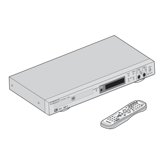
Page 9: Operating Controls And Functions
DV-SL8W OPERATING CONTROLS AND FUNCTIONS Main unit (front panel) ■ 1) Power Button 2) Microphone Volume Controls 3) Microphone Sockets 4) Stop Button PLAY STOP DVD PLAYER DV-SL8 POWER OPEN/CLOSE REMOTE 5) Play or Pause Button SENSOR SVCD – SKIP –... - Page 10 DV-SL8W ■ Remote control Remote Control Transmitter Setup Menu Button Subtitle Select Button Angle Select Button Interlace and Progressive Scan Direct Button OPEN/ SETUP CLOSE Resume Button Title Select Button SUBTITLE Zoom Button ANGLE 10. Cursor or Echo Level Up and Down Buttons 11.
-
Page 11: Troubleshooting
DV-SL8W TROUBLESHOOTING FLOW CHART NO. 1 The power cannot be turned on. Is the fuse normal? See FLOW CHART No. 2 <The fuse blows out.> Is normal state restored when once unplugged power Check if there is any leak or short-circuiting on the cord is plugged again after several seconds? primary circuit component, and service it if defective. - Page 12 DV-SL8W FLOW CHART NO. 6 P-ON (+12V) is not outputted. FLOW CHART NO. 6 P-ON (+12V) is not outputted. Is +12V voltage supplied to the kathode of D9? Check D9, B1 and the periphery circuit, and service it if defective.
- Page 13 DV-SL8W FLOW CHART NO. 9 No operation is possible from the remote control unit. Operation is possible from the DVD, but no operation is possible from the remote control unit. Is 5V voltage supplied to Pin(3) terminal ofthe infrared Check EV+5V line and service it if defective.
- Page 14 DV-SL8W FLOW CHART NO. 13 [No Disc] indicated. (When the focus servo is not functioning.) Replace the DVD Servo PWB. No improvement can be found. Original DVD Servo PWB is poor. Replace the DVD Mecha. FLOW CHART NO. 14 [No Disc] indicated. (When the laser beam does not light up.) Replace the DVD Servo PWB.
- Page 15 DV-SL8W FLOW CHART NO. 17 Audio is not outputted normally. Set the disc on the disc tray, and playback. Are the analog audio signal outputted from each pin of Check each line between IC U20 and IC U13 or IC U20? replace IC U20 or DVD MPEG PWB or DVD Mecha.
-
Page 16: Block Diagrams
DV-SL8W BLOCK DIAGRAMS... - Page 17 DV-SL8W...
-
Page 18: Schematic Diagrams / Ic's Pin Voltage
DV-SL8W SCHEMATIC DIAGRAMS / IC’S PIN VOLTAGE Standard Notes Notes: 1. Do not use the part number shown on these draw- WARNING ings for ordering. The correct part number is shown in the parts list, and may be slightly different or Many electrical and mechanical parts in this chassis amended since these drawings were prepared. - Page 19 DV-SL8W LIST OF CAUTION, NOTES, AND SYMBOLS USED IN THE SCHEMATIC DIAGRAMS ON THE FOLLOWING PAGES: 1. CAUTION: FOR CONTINUED PROTECTION AGAINST FIRE HAZARD, REPLACE ONLY WITH THE SAME TYPE FUSE. 2. CAUTION: Fixed Voltage (or Auto voltage selectable) power supply circuit is used in this unit.
- Page 20 DV-SL8W CN 18 P-12V R183 P+12V Servo analog +5V A+5V P+5V power R152 BC75 CON6-2.54 BC95 BC94 BC45 0.1U 0.1U 0.1U 0.1U MOTOR +5V power M+5V FB(300ma 0.7 ohm) EC34 BC68 100 U16V 0.1U P+5V DVCC3 LD1 117-3V3(1A) FB(300ma 0.7 ohm)
- Page 21 DV-SL8W RF 3.3V EC23 100 U16V PLL3.3V close to 8200 Servo PLL/slicer +3.3V power BC32 0.1U A3.3V BC33 0.1U PWM3.3 FB(300ma 0.7 OHM) BC25 0.1U AD POWER +3.3V AD_VCC3 R107 BC56 0.1U 100U10V deo PLL wer +1.8V VPLLVCC1 .8 SD_VCC3 FB(300ma 0.7 OHM)
- Page 22 DV-SL8W R117 R122 SANYO 1000P SANYO 1000P SANYO SAMSUNG 1000P SAMSUNG 3.3K 2700P SAMSU MITSUMI 1000P MITSUMI 3.3K 2700P M ITSUM SONY 310 1000P SONY 310 1500P SONY 3 THOMSON 1500P THOMSON 3.3K 2700P Thomso DMEA D FCO DTCO F CO...
- Page 23 DV-SL8W R124 2.2K SANYO 2.2K SCART_SIG SAMSUNG SCART_SIG SCART_DISPLAY SCART_DISPLAY 2.2K M ITSUMI AU_Mute AUDIO_MUTE 4 SONY 310 AU_LRCK AU_LRCK AU_BCK Thomson DMEA AU_BCK AU_XCK AU_XCK SPDIF_OUT SPDIF_OUT R124 7.5K R118 2.2K SPDCO TRAY- TRAY+ 0.1u VVCC3 0.1u VVCC3 G ND 0.1u...
- Page 24 DV-SL8W SONY R F 3.3V BC35 BC40 BC42 BC58 BC39 R F 3.3V R148 R150 0.1U 0.1U 0.1U 0.1U 0.1U C 87 C 85 SANYO 0.1u G ND C 86 R 185 1.2K (1%) SAMSUNG MITSUMI P U H RF...
- Page 25 DV-SL8W WF11 TP20 R F O R FO XRFRP TP28 R F RP R F RP SIPCLK P+5V SIPDATA SIPDEN G N D 0.1U R F 3.3V 8550(DIP ECB) 8550(DIP ECB) LOAD- R170 2.2K R 101 2.2K TP18 D FCT...
- Page 26 DV-SL8W +12V D VCC 820R SCART H9014 P+12V BEAD BEAD SCAR T_DISPLAY H9014 A F R R 11 G N D CVBS Pr(R) Y(G) Pb(B) G N D G N D D VCC D VCC D V C C D V C C...
- Page 27 DV-SL8W V+5V R 95 C 102 75(0805) WF8/WF9 C 49 BC105 BC106 D VCC 8550(DIP) C103 100P 100P R 94 G N D G N D G N D G N D 74HCU04 V+5V G N D BC107 BC108 R 89...
- Page 28 DV-SL8W 32VFD 4 NetLabel125 NetLabel126 -21V 16312 IN4148 RE 1 IN4148 REMOTE 1.15V 1.15V DA TA 1.15V C1.K 220U/10V R5 R6 R7 R8 10K 10K 10K 10K 10K 10K DATA Figure 9 FRONT PANEL SCHEMATIC DIAGRAM...
- Page 29 DV-SL8W Figure 10 POWER SCHEMATIC DIAGRAM...
- Page 30 DV-SL8W VOLTAGE CHART U13 (MPEG A/V PROCESSOR, SUNPLUS SPHE8200A) Ref.No. MODE STOP PLAY Ref.No. MODE STOP PLAY Ref.No. MODE STOP PLAY Ref.No. MODE STOP PLAY Ref.No. MODE STOP PLAY Ref.No. MODE STOP PLAY Ref.No. MODE STOP PLAY Ref.No. MODE STOP PLAY Ref.No.
- Page 31 DV-SL8W U17 ( SERVO IC, SUNPLUS SPHE6300A) Ref.No. MODE STOP PLAY Ref.No. MODE STOP PLAY Ref.No. MODE STOP PLAY Ref.No. MODE STOP PLAY Ref.No. MODE STOP PLAY U15 (MOTOR DRIVER IC, SM5954FP) Ref.No. MODE STOP PLAY Ref.No. MODE STOP PLAY U2 (OP AMP IC, SM4558) Ref.No.
-
Page 32: Waveforms
DV-SL8W WAVEFORMS VIDEO OUT S-VIDEO OUT - Y Output Video Out 0.5V 20us Video Y 0.2V 20us Note : S-VIDEO OUT - C Output WF1 ~ WF3 : Power On (Stop) Mode. WF4 ~ WF7 : DVD Test Disc TDV-540A. - Page 33 DV-SL8W COMPONENT VIDEO OUT - Pr/Cr Output COMPONENT VIDEO OUT - Pr/Cr Output (Interlace mode) (P-Scan mode) Interlace Mode Pr level : 525mV ±10% P-Scan Mode Pr level : 525mV ±10% 20us 20us WF10 Audio Left WF11 Audio Right Audio-L 2 ± 0.2Vrms Audio-R 2 ±...
-
Page 34: Wiring Diagram
DV-SL8W WIRING DIAGRAMS BC68 R181 R170 R101 R180 R179 R160 R144 R143 R155 R154 BC59 R186 R103 BC66 R104 R127 B C 3 0 R205 R182 BC28 BC32 BC27 BC78 BC25 BC22 BC52 BC31 BC20 BC92 R206 BC29 BC91 BC53... - Page 35 DV-SL8W R138 R137 R150 R148 BC75 BC40 R152 BC42 BC58 BC35 R151 BC69 R189 BC32 BC79 BC25 R172 R102 BC22 R173 BC93 R171 BC16 BC46 BC36 BC45 BC44 BC94 R183 BC10 BC95 BC17 B C 3 8 BC101 BC100 C105...
- Page 36 DV-SL8W Figure 2: WIRING SIDE OF SERVO PWB (3/5) SERVO PWB (PWB-C) EC28 VGA PORT SONY280 EC27 EC32 EC21 SL - SL + EC22 SP - SP + EC18 EC39 EC16 AUDIO OUTPUT +5V IR GND CLK STB DAT GND CEN SUB FL FR SL SR...
- Page 37 DV-SL8W Figure 4: WIRING SIDE OF SERVO PWB (4/5)
- Page 38 DV-SL8W Figure 5: WIRING SIDE OF SERVO PWB (5/5)
- Page 39 DV-SL8W DISPLAY PWB (PWB-A) (CNS 1) (CNS 7) FROM MIC PWB SERVO (CNS 6) (CNS 4) -21V SERVO PWB FROM POWER PWB LUG 2 TO CHASSIS GND (PWB-D) MIC PWB WH-WHITE (MIC 1) RD-RED (MIC 2) BK-BLACK (GND) TO DISPLAY...
- Page 40 DV-SL8W POWER PWB Brown Blue AC POWER SUPPLY CORD (AC1) AC 110/127/220/230~240V (50/60Hz) Figure 7: POWER PWB PATTERN...
-
Page 41: System Control Timing Charts
DV-SL8W SYSTEM CONTROL TIMING CHARTS Tray Close ~ Play / Play ~ Tray Open Tray Disc Play Tray Tray Close Rotation Stop Open 3.3V Tray IN (R143) 1.65V Sled Drive (IC U15 Pin 12) 1.65V Disc Drive (IC U15 Pin 18) 1.65V... -
Page 42: Ic Pin Function Descriptions
DV-SL8W IC PIN FUNCTION DESCRIPTIONS U1, Hex Inverter (Philips 74HCU04) Pin Configulation: Functional Diagram: 1A 1 Pin Description : PIN NO. SYMBOL NAME AND FUNCTION 1, 3, 5, 9, 11, 13 1A to 6A Data inputs 2, 4, 6, 8, 10, 12... - Page 43 DV-SL8W U10, EEPROM IC (AMTEL AT24C02N) Pin Configurations : Pin Description : Pin Name Function A0 - A2 Address Inputs Ground Supply Voltage Write Protect Serial Data Serial Clock Input Block Diagram : START STOP LOGIC SERIAL H.V. PUMP/TIMING CONTROL...
- Page 44 DV-SL8W U13, DVD SINGLE-CHIP MPEG A/V PROCESSOR (SPHE8200A) BLOCK DIAGRAM RISC PLLv PLLa EPROM/ Servo loader inf. icache dcache SRAM Power control EPROM/SRAM interface loader RF input Intr. control Graphics Engine Timer SDRAM SDRAM/16 or 32 controller IR/VFD/(I2C) Engine processor...
- Page 45 DV-SL8W GROUP MAP VSS_* VDD_* System CLKIN HGIN Interface RSTB LGIN1 TESTMODE LGIN2 LPFNIN PDFLT1 FDFLT AIN_L/MIC VREFO AIN_R PDRSET analog FDRSET interface DRESET SERVO CNIN SLVL AUI_BCK AUI_LRCK digital input RFRP AUI_DATA RFRPLP TEXOLP AU_XCK TEXO Audio AU_BCK digital output...
- Page 46 DV-SL8W SIGNAL STATE DESCRIPTION Supply Pins (51) VSS_ K* 30,47,79,100,124,142 Ground pins for chip kernel logic VSS_ O* 36,63,90,107,116,132,152 Ground pins for chip output VSS_K6/O7 Shared ground pin VDD_ K* 24,42,76,95,120,137,177 1.8V power supply pins for chip kernel logic and input pre-driver...
- Page 47 DV-SL8W SIGNAL STATE DESCRIPTION R_A19/GPIO ROM / SRAM/ Flash address bus bit 19 or GPIO Priority selection Function sft_cfg0[0]=1’b1 R_A19 (default) sft_cfg2[4:2]=3’b010 UART0 TX (Other) GPIO[32] R_OE_B/GPIO ROM / SRAM/ Flash output enable or GPIO Priority selection Function sft_cfg1[4]=1’b1 R_OE_B (default) sft_cfg4[2:0]=3’b100...
- Page 48 DV-SL8W SIGNAL STATE DESCRIPTION M_CLOKO SDRAM clock output M_CKE SDRAM clock enable M_A[11]/GPIO SDRAM address bus [11] or GPIO Priority selection Function sft_cfg6[4]=1’b1 M_A[11] (default) (Other) GPIO[14] M_A[9] SDRAM address bus [9] M_A[8] SDRAM address bus [8] M_A[7] SDRAM address bus [7]...
- Page 49 DV-SL8W SIGNAL STATE DESCRIPTION A_IEC_TX/GPIO IEC-958 transmit data Priority selection Function sft_cfg3[7]=1’b1 A_IEC_tX (default) (Other) GPIO[19] A_DATA[0] / GPIO Serial audio data output for channel 1/0 or GPIO Priority selection Function sft_cfg3[7]=1’b1 A_DATA[0] (default) (Other) GPIO[20] A_DATA[1] / GPIO Serial audio data output for channel 3/2 or GPIO...
- Page 50 DV-SL8W SIGNAL STATE DESCRIPTION VFD_DATA_TDM_CLK GIPO (for VFD data) or TDM clock This pin must be pull-high to 3.3V. Priority selection Function sft_cfg4[14:13]=2’b10 TDM_CLK (Other) GPIO[56] (default) UA0_RX/GPIO UART #0 data receive or GPIO Priority selection Function sft_cfg2[4:2]=3’b101 UART0_RX (default)
- Page 51 DV-SL8W SIGNAL STATE DESCRIPTION TDM_DX/ttin0_4/GPIO TDM output data or GPIO TDM_CLK/ttin1_5/GPIO TDM master clock or GPIO TDM_FSXR/ttin2_6/GPIO TDM input/output frame signal or GPIO TDM_DR/ttin3_7/GPIO/R_C_S4B TDM intput data or GPIO Servo Analog Interface (25) (Servo Analog Pins) (Servo Analog Pins) HGIN...
- Page 52 DV-SL8W U17, SERVO IC (SPHE6300A) PIN DESCRIPTIONS XOPVIP1 XTDM_DX XOPVIN1 XTDM_CLK XOPVOP1 XTDM_FSXR XOPVIP2 XTDM_DR XOPVIN2 XTDM0 XOPVOP2 XTDM1 AVSS XTDM2 XOPDA DVCC XDPDB XCLK XDPDC XDATA XDPDD AVDD XDOUT XDVDD DVSS XDVDC XRFRPPH XRFRPBH XDVDB AVDO XDVDA SPHE6300A XRFRPMEAN...
- Page 53 DV-SL8W PIN NO. PIN NAME TYPE DESCRIPTION XOPVIP1 Op-amp 1 positive input. XOPVIN1 Op-amp 1 negative input. XOPVOP1 Op-amp 1 output. XOPVIP2 Op-amp 2 positive input. XOPVIN2 Op-amp 2 negative input. XOPVOP2 Op-amp 2 output. AVSS Ground Power group 1 XDPDA AC coupled RF inputs for the DPD from the main beam photo detector.
- Page 54 DV-SL8W PIN NO. PIN NAME TYPE DESCRIPTION XGPOUT2 Digital output. XGPOUT1 XGPOUT0 DVCC Power Power group 5 XFEO Focus error signal output. XFEOCAP External capacitor connected to XFEO. XTEO Tracking error signal output. XTEOCAP External capacitor connected to XTEO. AVSS...
- Page 55 DV-SL8W U20, STEREO D/A CONVERTER (CS4334) PIN DESCRIPTIONS SDATA AOUTL SERIAL DATA INPUT ANALOG LEFT CHANNEL OUTPUT DEM/SCLK DE-EMPHASIS/SCLK ANALOG POWER LRCK AGND LEFT/RIGHT CLOCK ANALOG GROUND MCLK AOUTR MASTER CLOCK ANALOG RIGHT CHANNEL OUTPUT Pin Name Pin Function and description...
- Page 56 DV-SL8W IC1 (DISPLAY PWB), VFD DRIVER IC (ATC16312) Pin Assignment 43 42 41 40 29 38 37 36 35 34 S15/G6 S14/G7 ATC16312 S13/G8 S12/G9 -44QFP S11/G10 12 13 14 15 16 17 18 19 20 21 22 Pin Description Pin No.
-
Page 57: Fl Display
DV-SL8W FL DISPLAY MEC32, 92L38T02C01320 PATTERN: SVCD GRID ASSIGNMENT: SVCD PATTERN DETAILS: Icon2 Icon1... - Page 58 DV-SL8W MEC32, 92L38T02C01320 FL DISPLAY ANODE CONNECTION: Icon1 PAUSE PLAY Dolby logo Icon2 PIN CONNECTION: PIN NO. CONNECTION PIN NO. CONNECTION PIN NO. CONNECTION PIN NO. CONNECTION NOTES: F : Filament Grid NC : No Connection NP : No Pin...
-
Page 59: Lead Identifications
DV-SL8W LEAD IDENTIFICATION 1. EMITTER 1. EMITTER 1. EMITTER 2. BASE 2. BASE 2. BASE 3. COLLECTOR 3. COLLECTOR 3. COLLECTOR 1 2 3 1 2 3 1 2 3 Transistor S9015 (PNP) Transistor S9014 (NPN) Transistor S8550 (PNP) FIXED VERSION... - Page 60 DV-SL8W PARTS GUIDE DVD VIDEO PLAYER DV-SL8W MODEL CONTENTS [1] INTEGRATED CIRCUITS [10] CAPACITORS [2] IC PACKAGE SUPPLY PARTS [11] RESISTORS [3] TRANSISTORS [12] ARRAY PARTS [4] DIOEDS [13] OTHER CIRCUITRY PARTS [5] FILTERS [14] P.W.B. ASSEMBLY (Replacement Items) [6] TRANSFORMER...
- Page 61 DV-SL8W PRICE PART PARTS CODE DESCRIPTION RANK MARK RANK [1] INTERGRATED CIRCUITS 92L21TSL8W1631 VFD/FL Driver IC, AD16312(ATC16312) (Front Panel PWB) 92L22TSL8W2659 Switching IC, FairChild 5M02659R (Power PWB) 92L23TSL8W8170 Photocoupler, Liteon LTV-817 92L21TSL8W7404 HEX Inverter (14Pin), PHILIPS 74HCU04 U2,U6 92L21TSL8W4558 OP AMP IC (8Pin), SM4558...
- Page 62 DV-SL8W PRICE PART PARTS CODE DESCRIPTION RANK MARK RANK COILS 92L15EKFB00010 0Ω, Ferrite bead (0603) L36,L37 92L15EK1060000 10uH Inductor (0805) 92L15EK1050000 1uH Inductor (0603) (MPEG PWB) [8] VARIABLE RESISTORS W1,W2 92L07T02S10000 MIC Volume Control [9] VIBRATORS 92L18S01P02270 Crystal, 27.0000MHz [10] CAPACITORS...
- Page 63 DV-SL8W PRICE PART PARTS CODE DESCRIPTION RANK MARK RANK [10] CAPACITORS 92L01S06EM1050 1uF Chip Capacitor 92L01S06EK4700 47pF Chip Capacitor 92L01S06EM1030 0.01uF Chip Capacitor 92L01S06EK1020 1000pF Chip Capacitor 92L01S06EM1040 0.1uF Chip Capacitor 92L01S06EK6810 680pF Chip Capacitor 92L01S06EK2210 220pF Chip Capacitor 92L01S06EM1030 0.01uF Chip Capacitor...
- Page 64 DV-SL8W PRICE PART PARTS CODE DESCRIPTION RANK MARK RANK [11] RESISTORS 92L05T104EJ474 470KΩ 1/4W ±5%, Carbon resistor (Power PWB) 92L05T108EJ103 10KΩ 1/8W ±5%, Resistor (Front Panel PWB) 92L04S06EJ6800 68Ω, Chip Resistor 92L05T108EJ330 33Ω 1/8W ±5%, Carbon resistor (Power PWB) 92L05T108EJ103 10KΩ...
- Page 65 DV-SL8W PRICE PART PARTS CODE DESCRIPTION RANK MARK RANK [11] RESISTORS R124 92L04S06EJ7520 7.5KΩ, Chip Resistor R125 92L04S06EJ1010 100Ω, Chip Resistor R126 92L04S06EJ1030 10KΩ, Chip Resistor R128 92L04S06EJ5120 5.1KΩ, Chip Resistor R129 92L04S06EJ1030 10KΩ, Chip Resistor R130,R131 92L04S06EJ1R00 1Ω, Chip Resistor...
- Page 66 DV-SL8W PRICE PART PARTS CODE DESCRIPTION RANK MARK RANK [15] CABINET PARTS 92L43T09000000 SHARP Badge 92L41TSL8WS480 Front Panel 92L48T02S00000 Leg Cushion (φ10 x 2mm) 92L41TSL8WS030 FL Window 92L41TSL8WS010 Karaoke Volume Knob 92L41TSL8WS000 Power Button 92L48TS2000502 Cab cushion (20 x 5 x 1mm)
- Page 67 DV-SL8W EXPLODED VIEW 603x3 603x3 PWB-A 601x2 601x4 MEC32 603x3 601x2 601x2 610x3 From Power Switch From DETAIL-Mic Jack AC Cord MIC1 DETAIL-Bottom View MIC2 BEND THE FFC WITHIN LENGHT 80~82mm. PWB-D 602x7 FFC5 FFC1 Bend 227x2 605x2 605x2 PWB-C...
- Page 68 DV-SL8W © COPYRIGHT 2004 BY SHARP CORPORATION ALL RIGHTS RESERVED. No part of this publication may be reproduced, stored in a retrieval system, or transmitted in any form or by any means, electronic, mechanical, photocopying, recording, or otherwise, without prior written permission of the publisher.
Need help?
Do you have a question about the DV-SL8W and is the answer not in the manual?
Questions and answers