Table of Contents
Advertisement
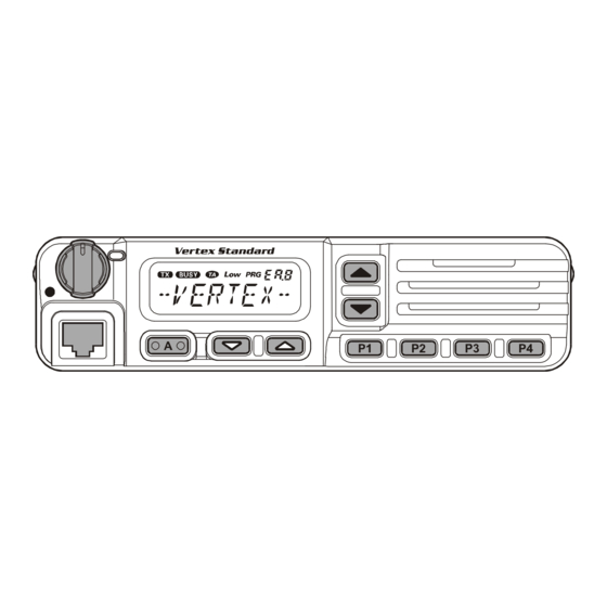
VHF FM Transceiver
VX-3200V
Service Manual
©
2002 VERTEX STANDARD CO., LTD.
Introduction
This manual provides technical information necessary for servicing the VX-3200V Transceiver.
Servicing this equipment requires expertise in handling surface-mount chip components. Attempts by non-qualified
persons to service this equipment may result in permanent damage not covered by the warranty, and may be illegal in
some countries.
Two PCB layout diagrams are provided for each double-sided circuit board in the transceiver. Each side of thr board is
referred to by the type of the majority of components installed on that side ("leaded" or "chip-only"). In most cases one
side has only chip components, and the other has either a mixture of both chip and leaded components (trimmers, coils,
electrolytic capacitors, ICs, etc.), or leaded components only.
While we believe the technical information in this manual to be correct, Vertex Standard assumes no liability for damage
that may occur as a result of typographical or other errors that may be present. Your cooperation in pointing out any
inconsistencies in the technical information would be appreciated.
Specifications ................................................... 2
Dsub 9-Pin Accessory Connector ................. 3
Exploded View & Miscellaneous Parts ........ 4
Block Diagram ................................................. 5
Interconnection Diagram ............................... 7
(EC039N90A)
Contents
Circuit Description ...................................... 9
Alignment ................................................... 11
Board Unit (Schematics, Layouts & Parts)
Rf Unit ............................................................................. 17
Panel Unit ........................................................................ 31
VERTEX STANDARD CO., LTD.
4-8-8 Nakameguro, Meguro-Ku, Tokyo 153-8644, Japan
VERTEX STANDARD
US Headquarters
10900 Walker Street, Cypress, CA 90630, U.S.A.
International Division
8350 N.W. 52nd Terrace, Suite 201, Miami, FL 33166, U.S.A.
YAESU EUROPE B.V.
P.O. Box 75525, 1118 ZN Schiphol, The Netherlands
YAESU UK LTD.
Unit 12, Sun Valley Business Park, Winnall Close
Winchester, Hampshire, SO23 0LB, U.K.
VERTEX STANDARD HK LTD.
Unit 5, 20/F., Seaview Centre, 139-141 Hoi Bun Road,
Kwun Tong, Kowloon, Hong Kong
1
Advertisement
Table of Contents

Related Manuals for Vertex Standard VX-3200V


Summary of Contents for Vertex Standard VX-3200V
- Page 1 ICs, etc.), or leaded components only. While we believe the technical information in this manual to be correct, Vertex Standard assumes no liability for damage that may occur as a result of typographical or other errors that may be present. Your cooperation in pointing out any inconsistencies in the technical information would be appreciated.
- Page 2 Specifications General Frequency range: 134-160 MHz (Version A) 148-174 MHz (Version C) Number of Groups: Number of Channels : 128 channels PLL Steps: 2.5 kHz / 5.0 kHz / 6.25kHz Power Supply Voltage: 13.6V DC ±15 % Channel Spacing: 12.5 / 15.0 / 25.0 / 30.0 kHz Current Consumption (Approx.): TX: 10 A RX: 700 mA...
- Page 3 DSUB 9-pin Accessory Connector Pin 1: Output Logic squelch (Will be effective this output during Data transmission – Inputting logic Low level signal to the Pin #4 as the DTR signal) High: Radio receiving the signal with the correct CTCSS or DCS. Low: Radio not receiving the signal with the correct CTCSS or DCS.
- Page 4 Exploded View & Miscellaneous Parts REF. VXSTD P/N DESCRIPTION QTY. „ • U20308002 BINDING HEAD SCREW M3 x 8 NI ‚ U24306002 TAPTITE SCREW M3 x 6 NI ƒ U24308002 TAPTITE SCREW M3 x 8 NI „ „ U31206007 OVAL HEAD SCREW M2.6 x 6 B CASE RA0015100 „...
- Page 5 Block Diagram (1)
- Page 6 Block Diagram (2)
- Page 7 Interconnection Diagram...
- Page 8 Note...
- Page 9 Circuit Description 1. Overview Detected audio from Q1029 is applied to Q2016 (AK2345) and audio low-pass filter. After volume adjustment by The VX-3200V is a VHF/FM mobile transceiver designed Q2014 (M62364FP), the audio signal is amplified by the to operate in the frequency range of 148 to 174MHz(C AF power amplifier Q1509 (TDA2003H) and passed to Band), or 134 to 160MHz(A Band).
-
Page 10: Power Supply Circuits
Circuit Description 7. Power Supply Circuits for providing to the first local signal. In TX, the VCO gen- erates 148 to 174MHz (C Band), 134 to 160MHz (A Band). 7-1 All 13.6V 13.8V is always supplied to Power AMP Q1039 The output of the VCO is amplified by the Q1020 and rout- (RA45H4452M). - Page 11 Vertex Standard VPL-1 Connection Cable & We recommend that servicing be performed only by au- Alignment program thorized Vertex Standard service technicians who are ex- Alignment Preparation & Precautions perienced with the circuitry and fully equipped for repair and alignment. Therefore, if a fault is suspected, contact...
- Page 12 Alignment PLL VCV Setup the test equipment as shown below, apply 13.6V DC power to the transceiver. ¦ Connect the positive lead of the DC voltmeter to the test point TP1007 (VCV) on the RF-Unit, as The transceiver must be programmed for use in the in- indicated in the figure, and the negative lead to tended system before alignment is attempted.
- Page 13 Alignment The alignment tool outline Menu of the tool Installation the tool [0] Common TX This alignment tool consists, MS-DOS based, only one ex- - [0] Tx Power High ecute file “svc52.exe.“ You make a directly as you think This parameter is used to align TX High power (50 W). fit, and copy this file.
- Page 14 Alignment - [3] REF Deviation [1] Common RX This parameter is used to align the REF Deviation. - [0] Tight NSQL ¦ Press [Enter] on “[3] REF Deviation” to align REF This parameter is used to align the noise level in squelch Deviation.
- Page 15 RF Unit Jumper Information JP1501 (JP1): Determine the o u t p u t s u p p l y voltage at pin 8 of DSUB 9-pin Ac- cessory Connector. Close: +5.0 V (Maximum 100 mA) Open: No Action JP1502 (JP2): Determine the output supply volt- age at pin 8 of DSUB 9-pin Acces- sory Connector.
- Page 16 Note...
- Page 17 RF Unit Circuit Diagram (1) HIGH POWER: 0.4 V LOW POWER: 0.1 V RX: 0 V TX: 1.6 V RSSI: 0.6 ~ 2.4 V RX: 0 V RX: 0 V RX: 0 V TX: 2.0 V TX: 7.0 V RX: 0 V TX: 8.1 V TX: 2.0 V 5.0 V...
- Page 18 RF Unit Circuit Diagram (2) 4.8 V 2.2 V 1.2 V 0.7 V 1.3 V RX WIDE: 0.2 ~ 3.8 V RX NARROW: 0.2 ~ 3.5 V TX: 0.2 V RX WIDE: 0.8 ~ 3.8 V RX NARROW: 0.8 ~ 3.1 V RX: 0.3 V TX: 0.8 V TX: 0 V...
- Page 19 RF Unit Parts Layout (Side A) RA60H1317M TDA2003H MB15A02PFV1 (Q1039) (Q1509) (Q1023) NJM2902V M5223 2SA1162GR (SG) (Q1503) (Q1019) (Q1035) 2SA1602A (MF) (Q1031) 2SC2712 (LG) 2SJ125D (JD) 2SK520 (K41) (Q1036) (Q1515) (Q1013) 2SC3356 (R24) (Q1011, 1037) 2SC4154 (LE) R1055 (Q1034, 1501) R1190 2SC4226 (R22) (Q1011, 1015)
- Page 20 RF Unit Parts Layout (Side B) TA31136FN NJM2902V 2SB1201S (Q1028) (Q1003) (Q1005) 2SA1602A (MF) 2SB1132 (BA) 2SB1301 (ZQ) (Q1505) (Q1009) (Q1511) 2SD1368CB (CB) (Q1504) 2SC4154 (LE) 2SC5415E (EA) DTB123EK (F12) (Q1501, 1007, 1519) (Q1025) (Q1008) 2SC4215 (QY) (Q1029) 2SC5107 (MF0) (Q1020, 1021, 1026) IMH6A (H6) MM1216ENRE...
-
Page 21: Parts List
RF Unit Parts List DESCRIPTION VALUE TOL. MFR'S DESIG VXSTD P/N VERS. LOT SIDE LAY ADR PCB with Component (w/o Q1039) CB1946001 Printed Circuit Board FR008050B C 1001 CHIP CAP. 0.001uF 630V GHM1030R102K630PT K22281801 C 1002 CHIP CAP. 220pF GRM39CH221J50PT K22174243 C 1002 CHIP CAP. - Page 22 RF Unit Parts List DESCRIPTION VALUE TOL. MFR'S DESIG VXSTD P/N VERS. LOT SIDE LAY ADR C 1079 CHIP TA.CAP. 10uF TEMSVA1A106M-8R K78100028 C 1080 CHIP CAP. 0.01uF GRM39B103M50PT K22174823 C 1081 CHIP CAP. 0.1uF GRM39B104K16PT K22124805 C 1082 CHIP CAP. 0.01uF GRM39B103M50PT K22174823...
- Page 23 RF Unit Parts List DESCRIPTION VALUE TOL. MFR'S DESIG VXSTD P/N VERS. LOT SIDE LAY ADR C 1159 CHIP CAP. 12pF GRM39CH120J50PT K22174213 C 1160 CHIP CAP. 0.001uF GRM39B102K50PT K22174821 C 1161 CHIP CAP. 18pF GRM39CH180J50PT K22174217 C 1162 CHIP CAP. 0.01uF GRM39B103M50PT K22174823...
- Page 24 RF Unit Parts List DESCRIPTION VALUE TOL. MFR'S DESIG VXSTD P/N VERS. LOT SIDE LAY ADR C 1241 CHIP CAP. 22pF GRM39CH220J50PT K22174219 C 1242 CHIP CAP. 100pF GRM39CH101J50PT K22174235 C 1243 CHIP CAP. 100pF GRM39CH101J50PT K22174235 C 1244 CHIP CAP. 100pF GRM39CH101J50PT K22174235...
- Page 25 RF Unit Parts List DESCRIPTION VALUE TOL. MFR'S DESIG VXSTD P/N VERS. LOT SIDE LAY ADR C 1527 CHIP CAP. 0.1uF GRM39B104K16PT K22124805 C 1528 CHIP CAP. 0.1uF GRM39B104K16PT K22124805 C 1529 CHIP CAP. 470pF GRM39CH471J50PT K22174249 C 1530 CHIP CAP. 470pF GRM39CH471J50PT K22174249...
- Page 26 RF Unit Parts List DESCRIPTION VALUE TOL. MFR'S DESIG VXSTD P/N VERS. LOT SIDE LAY ADR L 1010 M.RFC 0.47uH C2012C-R47J L1691016 L 1011 M.RFC 0.47uH C2012C-R47J L1691016 L 1012 M.RFC 10uH LK1608 100K-T L1690689 L 1013 COIL 0.033uH AS1005-33NK L0022546 L 1014 COIL...
- Page 27 RF Unit Parts List DESCRIPTION VALUE TOL. MFR'S DESIG VXSTD P/N VERS. LOT SIDE LAY ADR Q 1507 TRANSISTOR RT1N241M-T11-1 G3070249 Q 1508 TRANSISTOR PDTC114TE G3070238 Q 1509 TDA2003H G1090815 Q 1510 TRANSISTOR PDTC114TE G3070238 Q 1511 TRANSISTOR 2SB1301-T2 ZQ G3213017Q Q 1512 TRANSISTOR...
- Page 28 RF Unit Parts List DESCRIPTION VALUE TOL. MFR'S DESIG VXSTD P/N VERS. LOT SIDE LAY ADR R 1067 CHIP RES. 4.7k 1/16W RMC1/16 472JATP J24185472 R 1068 CHIP RES. 1.2k 1/16W RMC1/16 122JATP J24185122 R 1069 CHIP RES. 1/16W RMC1/16 103JATP J24185103 R 1070 CHIP RES.
- Page 29 RF Unit Parts List DESCRIPTION VALUE TOL. MFR'S DESIG VXSTD P/N VERS. LOT SIDE LAY ADR R 1155 CHIP RES. 1/10W RMC1/10T 390J J24205390 R 1156 CHIP RES. 1/16W RMC1/16 221JATP J24185221 R 1157 CHIP RES. 180k 1/16W RMC1/16 184JATP J24185184 R 1158 CHIP RES.
- Page 30 RF Unit Parts List DESCRIPTION VALUE TOL. MFR'S DESIG VXSTD P/N VERS. LOT SIDE LAY ADR R 1550 CHIP RES. 1/16W RMC1/16 333JATP J24185333 R 1551 CHIP RES. 4.7k 1/16W RMC1/16 472JATP J24185472 R 1553 CHIP RES. 1/16W RMC1/16 473JATP J24185473 R 1554 CHIP RES.
- Page 31 PANEL Unit Circuit Diagram 5.0 V 1.3 V 1.8 V 2.3 V 1.8 V 1.0 V 1.3 V 2.6 V LIGHT ON: 3.9 V LIGHT OFF: 0 V TX: 1.8 V BUSY: 2.2 V 0.8 V 3.2 V 0.8 V 5.0 V 0.6 V 0.8 V...
-
Page 32: Panel Unit
PANEL Unit Parts Layout (Side A) LC87F72C8A BU4066BF S-93C56AMFN (Q2003) (Q2024) (Q2011) S-80835CNMC 2SC4617 (BR) BRPG1211C (Q2003) (Q2004, 2020) (D2004) DA221 (K) MC2846 (A4) (D2003, 2033, 2034) (D2011) Parts Layout (Side B) AK2345 LA8630M NJM2902V (Q2016) (Q2017) (Q2015, 2021, 2022) M62364FP (Q2014) D2035... - Page 33 PANEL Unit Parts List DESCRIPTION VALUE TOL. MFR'S DESIG VXSTD P/N VERS. LOT SIDE LAY ADR PCB with Component CB1947001 Printed Circuit Board FR007630D C 2001 CHIP CAP. 0.1uF LMK105BJ104KV-F K22108806 C 2002 CHIP TA.CAP. 10uF 6.3V TEMSVA0J106M-8R K78080027 C 2003 CHIP CAP.
- Page 34 PANEL Unit Parts List DESCRIPTION VALUE TOL. MFR'S DESIG VXSTD P/N VERS. LOT SIDE LAY ADR C 2083 CHIP CAP. 820pF UMK105B821KW-F K22178828 C 2085 CHIP TA.CAP. 10uF 6.3V TEMSVA0J106M-8R K78080027 C 2086 CHIP CAP. 0.01uF GRM36B103K16PT K22128804 C 2087 CHIP CAP.
- Page 35 PANEL Unit Parts List DESCRIPTION VALUE TOL. MFR'S DESIG VXSTD P/N VERS. LOT SIDE LAY ADR R 2161 CHIP RES. 120k 1/16W RMC1/16S 124JTH J24189050 R 2162 CHIP RES. 1/16W RMC1/16S 823JTH J24189048 R 2163 CHIP RES. 1/16W RMC1/16S 221JTH J24189017 R 2164 CHIP RES.
- Page 36 PANEL Unit Parts List DESCRIPTION VALUE TOL. MFR'S DESIG VXSTD P/N VERS. LOT SIDE LAY ADR Q 2020 TRANSISTOR 2SC4617 TL R G3346178R Q 2021 NJM2902V-TE1 G1091679 Q 2022 NJM2902V-TE1 G1091679 Q 2024 BU4066BF-E2 G1092593 Q 2025 TRANSISTOR RT1N241M-T11-1 G3070249 Q 2026 TRANSISTOR PDTC114TE...
- Page 37 PANEL Unit Parts List DESCRIPTION VALUE TOL. MFR'S DESIG VXSTD P/N VERS. LOT SIDE LAY ADR R 2070 CHIP RES. 1/16W RMC1/16S 473JTH J24189045 R 2071 CHIP RES. 1.5M 1/16W RMC1/16S 155JTH J24189063 R 2072 CHIP RES. 1.5k 1/16W RMC1/16S 152JTH J24189027 R 2073 CHIP RES.
- Page 38 PANEL Unit Parts List Note DESCRIPTION VALUE TOL. MFR'S DESIG VXSTD P/N VERS. LOT SIDE LAY ADR...
- Page 40 Copyright 2002 VERTEX STANDARD CO., LTD. All rights reserved. No portion of this manual may be reproduced without the permission of VERTEX STANDARD CO., LTD.
Need help?
Do you have a question about the VX-3200V and is the answer not in the manual?
Questions and answers