Vertex Standard VX-600 Service Manual
Uhf band
Hide thumbs
Also See for VX-600:
- Specifications (4 pages) ,
- Operating manual (20 pages) ,
- Service manual (58 pages)
Table of Contents
Advertisement
Quick Links
VX-600
UHF Band
Service Manual
©2007 VERTEX STANDARD CO., LTD.
Operating Manual Reprint ................................................................................................................................................ 2
Cloning ................................................................................................................................................................................ 10
Specifications ..................................................................................................................................................................... 11
Exploded View & Miscellaneous Parts ......................................................................................................................... 12
Block Diagram .................................................................................................................................................................... 13
Circuit Description ............................................................................................................................................................ 14
Alignment ........................................................................................................................................................................... 17
Test Adapter Schematic .................................................................................................................................................... 23
Board Units (Schematics, Layouts & Parts)
MAIN Unit ...................................................................................................................................................................... 25
VR Unit ............................................................................................................................................................................ 57
SW Unit ............................................................................................................................................................................ 58
Dummy Unit ................................................................................................................................................................... 59
Optional Board Units (Schematics, Layouts & Parts)
F2D-8 2-Tone Decode Unit ............................................................................................................................................ 60
VTP-50 VX-Trunk Unit .................................................................................................................................................. 62
FVP-25 Encryption / DTMF Pager Unit ...................................................................................................................... 64
F5D-14 5-Tone Unit ........................................................................................................................................................ 66
E014U95A
Introduction
This manual describes the circuit theory, program-
ming procedures, and alignment procedures for the
Much of the operating flexibility of the
derived from its versatile "Soft Key" front panel keys.
These keys may be configured for a number of op-
erating functions, as described in this manual.
Following the discussion of transceiver operation,
details regarding programming software, alignment,
and maintenance will follow.
Contents
VERTEX STANDARD CO., LTD.
4-8-8 Nakameguro, Meguro-Ku, Tokyo 153-8644, Japan
VERTEX STANDARD
US Headquarters
10900 Walker Street, Cypress, CA 90630, U.S.A.
YAESU EUROPE B.V.
P.O. Box 75525, 1118 ZN Schiphol, The Netherlands
YAESU UK LTD.
Unit 12, Sun Valley Business Park, Winnall Close
Winchester, Hampshire, SO23 0LB, U.K.
VERTEX STANDARD HK LTD.
Unit 5, 20/F., Seaview Centre, 139-141 Hoi Bun Road,
Kwun Tong, Kowloon, Hong Kong
VERTEX STANDARD ( AUSTRALIA ) PTY., LTD.
Normanby Business Park, Unit 14/45 Normanby Road
Notting Hill 3168, Victoria, Australia
UHF Portable Transceiver.
is
1
Advertisement
Table of Contents

Related Manuals for Vertex Standard VX-600


Summary of Contents for Vertex Standard VX-600
-
Page 1: Table Of Contents
VERTEX STANDARD HK LTD. Service Manual Unit 5, 20/F., Seaview Centre, 139-141 Hoi Bun Road, Kwun Tong, Kowloon, Hong Kong VERTEX STANDARD ( AUSTRALIA ) PTY., LTD. Normanby Business Park, Unit 14/45 Normanby Road ©2007 VERTEX STANDARD CO., LTD. E014U95A... -
Page 2: Operating Manual Reprint
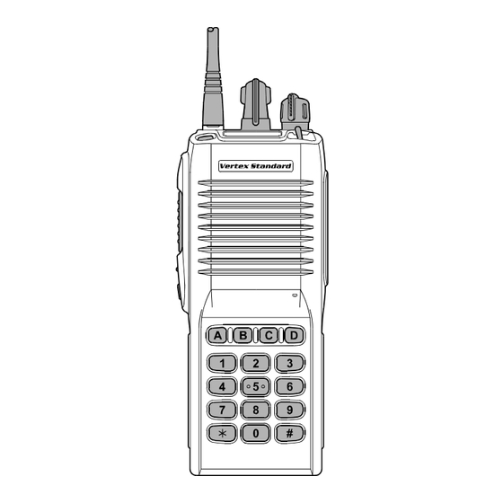
Operating Manual Reprint & C ONTROLS ONNECTORS CH ( Channel ) Selector LED Indicator Steady Green: Signaling off (or Scan active) Blinking Green: Busy Channel (or Squelch off) Steady Red: Transmission in Progress Antenna Jack Blinking Red: Battery voltage is low Blinking Yellow: Receiving a Selective Call TOP SEL (Selector) Key VOL/PWR (Volume/Power) Knob... - Page 3 “Click.” the basic operation of the VX-600. Tilt the Belt Clip Operation Quick Start Turn the top panel’s VOL/ PWR knob clockwise to turn on the radio on.
- Page 4 Operating Manual Reprint button more than 2 seconds (or press the MONI- Switch the top panel’s TOR button twice) to quiet the noise and resume TOGGLE switch to the normal (quiet) monitoring. [A], [B] or [Center] posi- tion to activate one of the To transmit, press and pre-programmed func- hold the PTT switch.
- Page 5 PERATION Soft key and TOGGLE switch Functions TOGGLE switch ( Position ) The VX-600 includes the [ TOP SEL ] , [ SIDE SEL ] , Functions center [ MONITOR ] , and [ LAMP ] keys, and the TOGGLE...
- Page 6 Operating Manual Reprint DVANCED PERATION High/Low Power Description of Operating Functions Press the assigned Soft key or switch the Toggle Channel Scan switch to the assigned position to set the radio’s trans- The Scanning feature is used to monitor multiple sig- mitter to the “Low Power”...
- Page 7 Channel Group Selection Switch the TOGGLE switch to lock the top-panel keys; The VX-600 is capable of separating its 48 memory this can be enabled to prevent radio settings from be- channels into any of 3 Groups. There is no limit as to ing disturbed.
- Page 8 Operating Manual Reprint DVANCED PERATION ARTS (Auto Range Transpond System) DTMF Paging System This system is designed to inform you when you and This system allows paging and selective calling, us- another ARTS-equipped station are within commu- ing DTMF tone sequences. nication range.
- Page 9 UHF Antenna, 450 ~ 485 MHz VH-120 3-Wire Earpiece, Mic, Palm PTT Switch Availability of accessories may vary; some accessories are supplied standard per local requirements, others may be unavailable in some regions. Check with your VERTEX STANDARD Dealer for changes to the this list.
-
Page 10: Cloning
Cloning includes a convenient “Clone” feature, 7. If there is a problem during the cloning process, which allows the programming data from one trans- sound an error beep from source the transceiver. ceiver to be transferred to another . Here is Check your cable connections and battery volt- the procedure for Cloning one radio’s data to anoth- age, and try again. -
Page 11: Specifications
Specifications ENERAL Frequency Range: 400 - 430 MHz (AS1), 440 - 470 MHz (CS), 450 - 485 MHz(D), 485 - 512 MHz (F) Number of Channels: 48 channels Channel Spacing: 12.5 / 25 kHz PLL Steps: 5 / 6.25 kHz Power Supply Voltage: 7.4 VDC ±20% Battery Life (5-5-90 duty):... -
Page 12: Exploded View & Miscellaneous Parts
Exploded View & Miscellaneous Parts RA0297600 CP6953004 EXT CAP FRONT CASE ASS'Y (16KEY) RA0215400 RA0297300 SHEET HOOK RA0306900 (x2 pcs) COIL SPRING RA030720A KNOB CP6953003 RA0343500 FRONT CASE ASS'Y (KEYLESS) RUBBER KNOB RA0317300 RA030770B RA0297000 LIGHT SHEET B KNOB M4090153 LATCH PLATE SPEAKER RA0317000... -
Page 13: Block Diagram
Block Diagram... -
Page 14: Circuit Description
Circuit Description , ±5.5 kHz BW) to strip Overview away all undesired mixer products. is a UHF FM hand-held transceiver de- signed to operate in the frequency range of 400 to IF Amplifier 512 MHz. The first IF signal is amplified by Circuit Configuration by Frequency The amplified first IF signal is applied to FM IF sub- The receiver is a double-conversion superheterodyne... - Page 15 Circuit Description The resulting DC squelch control voltage is passed If a CDCSS code is enabled for transmission, the code to pin 19 of the microprocessor . If no carrier is generated by and delivered to is received, this signal causes pin 6 of ) for CDCSS modulation.
- Page 16 Circuit Description Transmit Inhibit utilizing a 40 or 50 kHz reference signal which is When the Transmit PLL is unlocked, pin 18 of PLL eighth multiple of the channel step size (5, 6.25 or chip goes to logic "low." The resulting DC 7.5 kHz).
-
Page 17: Alignment
IBM PC / compatible Computer with Microsoft undertake any of the following alignments are cau- DOS v3.0 or later operating system tioned to proceed at their own risk. Problems caused Vertex Standard Connection Cable and by unauthorized attempts at realignment are not SVC39 Alignment program covered by the warranty policy. - Page 18 Alignment The alignment tool outline Whenever possible, alignments should be made with Installation of the Alignment Tool oscillator shields and circuit boards firmly affixed in place. Also, the test equipment must be thoroughly The “alignment mode” is a software-based protocol, warmed up before beginning.
- Page 19 Alignment (0) Common Tx : Alignment Sequence Although the data displayed on the computer’s The first alignment section adjusts transmit-mode screen during alignment is temporary data, it is im- parameters which are common to all channels. portant that you follow the basic alignment sequence - [0] F precisely, so that the displayed data and the data REQUENCY...
- Page 20 Alignment - [3] L2 - [6] MIC G This parameter is used to align MIC Gain level. This parameter aligns the L2 power (1 W) level. From the “ ” section, press [ ] to From the “ ” section, press [ ] to ac- tivate this alignment sequence.
- Page 21 Alignment Channels (1) Common RX : - [0] T The following parameters may be adjusted individu- IGHT OISE QUELCH This parameter is used to align the “ ally for each channel. For example, minor variations ” level. From the “” ”...
- Page 22 Alignment (3) Channels Rx : - [2] M AXIMUM EVIATION This parameter is to trim maximum deviation on - [0] M ANUAL UNING the displayed channel. From the “ This parameter is used to tune the RF front-end ” section, select [ ] to adjust the deviation level. components for the current channel manually.
-
Page 23: Test Adapter Schematic
Test Adapter Schematic Connector Pinout Diagram Pin 1 ( Pin 3 (GND) Pin 2 ( Pin 5 (Select) Pin 4 (MIC) Pin 7 (Clone) AF Test Adapter Schematic Attenuated White (Pin 1: Speaker +) Test Output (1/2) 220µF AF Output 16-ohm 220µF Blue (Pin 2: Speaker -) - Page 24 Note...
-
Page 25: Main Unit
Main Unit (Lot. 1 ~ 4) Circuit Diagram... - Page 26 Main Unit (Lot. 1 ~ 4) Note...
- Page 27 Main Unit (Lot. 1 ~ 4) Parts Layout (Side A) UMC5N (C5) NJM2902V CPH6102 (AB) UMG2N (G2) 2SA1774 (FR) PDTC144EE (26) TDA2822D (Q1018, 1022, 1058) (Q1008, 1037) (Q1014) (Q1017, 1020) (Q1019, 1024) (Q1015) (Q1007,1011) S-80735SN-DZ (DZ) XN1501 (5R) TK71635SCL (L35) S-93C56AMFN 2SC4617 (BR) UN911F (60)
- Page 28 Main Unit (Lot. 1 ~ 4) Parts Layout (Side B) XP1501 (5R) UMZ2N (Z2) 2SD1767 (DC) PDTC114TE TK71650SCL (L50) UN911F (60) CPH6102 (AB) UMG2N (G2) (Q1001) (Q1002) (Q1003) (Q1004) (Q1005) (Q1006, 1010, 1028, (Q1009) (Q1013, 1025) 1031, 1039) 2SC3356 (R24) (Q1026) 2SC4227 (R32) (Q1041)
- Page 29 Main Unit (Lot. 5 ~ 24) Circuit Diagram...
- Page 30 Main Unit (Lot. 5 ~ 24) Note...
- Page 31 Main Unit (Lot. 5 ~ 24) Parts Layout (Side A) UMC5N (C5) NJM2902V CPH6102 (AB) UMG2N (G2) 2SA1774 (FR) PDTC144EE (26) TDA2822D (Q1018, 1022, 1058) (Q1008, 1037) (Q1014) (Q1017, 1020) (Q1019, 1024) (Q1015) (Q1007,1011) S-80735SN-DZ (DZ) XN1501 (5R) TK71635SCL (L35) S-93C56AMFN 2SC4617 (BR) UN911F (60)
- Page 32 Main Unit (Lot. 5 ~ 24) Parts Layout (Side B) XP1501 (5R) UMZ2N (Z2) 2SD1767 (DC) PDTC114TE TK71650SCL (L50) UN911F (60) CPH6102 (AB) UMG2N (G2) (Q1001) (Q1002) (Q1003) (Q1004) (Q1005) (Q1006, 1010, 1028, (Q1009) (Q1013, 1025) 1031, 1039) 2SC3356 (R24) (Q1026) 2SC4227 (R32) (Q1041)
- Page 33 Main Unit (Lot. 25 ~) Circuit Diagram...
- Page 34 Main Unit (Lot. 25 ~) Note...
- Page 35 Main Unit (Lot. 25 ~) Parts Layout (Side A) UMC5N (C5) NJM2902V CPH6102 (AB) UMG2N (G2) 2SA1774 (FR) PDTC144EE (26) TDA2822D (Q1018, 1022, 1058) (Q1008, 1037) (Q1014) (Q1017, 1020) (Q1019, 1024) (Q1015) (Q1007,1011) S-80735SN-DZ (DZ) XN1501 (5R) TK71635SCL (L35) S-93C56AMFN 2SC4617 (BR) UN911F (60) LC87F72C8A...
- Page 36 Main Unit (Lot. 25 ~) Parts Layout (Side B) XP1501 (5R) UMZ2N (Z2) 2SD1767 (DC) PDTC114TE TK71650SCL (L50) UN911F (60) CPH6102 (AB) UMG2N (G2) (Q1001) (Q1002) (Q1003) (Q1004) (Q1005) (Q1006, 1010, 1028, (Q1009) (Q1013, 1025) 1031, 1039) 2SC3356 (R24) (Q1026) 2SC4227 (R32) (Q1041) 2SC4617 (BR)
- Page 37 Main Unit Parts List REF. DESCRIPTION VALUE TOL. MFR’S DESIG VXSTD P/N VERS. LOT. SIDE LAY ADR PCB with Components (W/ VR-UNIT) CP6946002 VERSION D CP6946004 VERSION A CP6946006 VERSION CS CP6946012 VERSION F Printed Circuit Board FR006560C Printed Circuit Board FR006560D 5-24 Printed Circuit Board...
- Page 38 Main Unit Parts List REF. DESCRIPTION VALUE TOL. MFR’S DESIG VXSTD P/N VERS. LOT. SIDE LAY ADR C 1025 CHIP CAP. 0.5pF GRM1554C1HR50BZ01D K22178285 VERSION F C 1026 CHIP CAP. GRM1552C1H9R0DZ01D K22178211 C 1026 CHIP CAP. GRM1552C1H8R0DZ01D K22178210 VERSION CS 7- C 1026 CHIP CAP.
- Page 39 Main Unit Parts List REF. DESCRIPTION VALUE TOL. MFR’S DESIG VXSTD P/N VERS. LOT. SIDE LAY ADR C 1053 CHIP CAP. GRM40B105K10PT K22100802 C 1053 CHIP CAP. GRM40B105K10PT(0.85) K22100803 C 1054 CHIP CAP. 0.01uF GRM36B103K16PT K22128804 C 1055 CHIP CAP. 150pF GRM1552C1H151JA01D K22178240...
- Page 40 Main Unit Parts List REF. DESCRIPTION VALUE TOL. MFR’S DESIG VXSTD P/N VERS. LOT. SIDE LAY ADR C 1104 CHIP TA.CAP. 4.7uF 6.3V TEMSVA0J475M-8R K78080017 C 1105 CHIP CAP. 22pF GRM1552C1H220JZ01D K22178220 C 1105 CHIP CAP. 27pF GRM1552C1H270JZ01D K22178222 VERSION CS 7- C 1105 CHIP CAP.
- Page 41 Main Unit Parts List REF. DESCRIPTION VALUE TOL. MFR’S DESIG VXSTD P/N VERS. LOT. SIDE LAY ADR C 1139 CHIP CAP. GRM1552C1H6R0DZ01D K22178208 C 1140 CHIP TA.CAP. TMCSA1C105MTR K78120023 C 1141 CHIP CAP. 120pF GRM1552C1H121JA01D K22178238 C 1143 CHIP CAP. 0.01uF GRM36B103K16PT K22128804...
- Page 42 Main Unit Parts List REF. DESCRIPTION VALUE TOL. MFR’S DESIG VXSTD P/N VERS. LOT. SIDE LAY ADR C 1199 CHIP CAP. GRM1554C1H2R0BZ01D K22178289 C 1201 CHIP CAP. 0.01uF GRM36B103K16PT K22128804 C 1202 CHIP TA.CAP. 10uF 6.3V EEJK0JS106R K78080079 C 1202 CHIP TA.CAP. 10uF 6.3V EEJK0JS106R...
- Page 43 Main Unit Parts List REF. DESCRIPTION VALUE TOL. MFR’S DESIG VXSTD P/N VERS. LOT. SIDE LAY ADR C 1236 CHIP CAP. GRM1552C1H6R0DZ01D K22178208 C 1236 CHIP CAP. GRM1552C1H6R0DZ01D K22178208 VERSION CS 8- C 1236 CHIP CAP. GRM1552C1H6R0DZ01D K22178208 VERSION A C 1236 CHIP CAP.
- Page 44 Main Unit Parts List REF. DESCRIPTION VALUE TOL. MFR’S DESIG VXSTD P/N VERS. LOT. SIDE LAY ADR C 1284 CHIP CAP. 0.001uF GRM155B11H102KA01D K22178809 C 1285 CHIP CAP. 0.1uF GRM155B11A104KA01D K22108802 C 1286 CHIP CAP. 0.1uF GRM155B11A104KA01D K22108802 C 1287 CHIP CAP. 0.1uF GRM155B11A104KA01D K22108802...
- Page 45 Main Unit Parts List REF. DESCRIPTION VALUE TOL. MFR’S DESIG VXSTD P/N VERS. LOT. SIDE LAY ADR CF1002 CERAMIC FILTER ELFY450G H3900551 D 1001 DIODE DA221 TL G2070178 D 1002 DIODE MA2S111-(TX) G2070614 D 1003 DIODE MA2S111-(TX) G2070614 D 1004 DIODE MA2S111-(TX) G2070614 D 1005 DIODE...
- Page 46 Main Unit Parts List REF. DESCRIPTION VALUE TOL. MFR’S DESIG VXSTD P/N VERS. LOT. SIDE LAY ADR D 1058 DIODE DA221 TL G2070178 D 1059 DIODE DA221 TL G2070178 D 1060 DIODE MA132WK-(TX) G2070776 D 1061 DIODE HVC350B-TRF-E G2070596 D 1062 DIODE HVC350B-TRF-E G2070596 F 1001 CHIP FUSE...
- Page 47 Main Unit Parts List REF. DESCRIPTION VALUE TOL. MFR’S DESIG VXSTD P/N VERS. LOT. SIDE LAY ADR L 1029 M.RFC 0.68uH LK1608 R68K-T L1690416 L 1029 M.RFC 0.56uH LK1608 R56K-T L1690415 L 1030 M.RFC 0.082uH HK1608 82NJ-T L1690527 L 1031 M.RFC 0.082uH HK1608 82NJ-T L1690527...
- Page 48 R 1006 CHIP RES. 1/16W 5% RMC1/16S 102JTH J24189025 R 1007 CHIP RES. 1/16W 5% RMC1/16S 103JTH J24189037 R 1008 CHIP RES. 8.2k 1/16W 5% RMC1/16S 822JTH J24189036 R 1009 CHIP RES. 1/16W 5% RMC1/16S 102JTH J24189025 Please contact VERTEX STANDARD.
- Page 49 Main Unit Parts List REF. DESCRIPTION VALUE TOL. MFR’S DESIG VXSTD P/N VERS. LOT. SIDE LAY ADR R 1010 CHIP RES. 1/16W 5% RMC1/16S 102JTH J24189025 R 1011 CHIP RES. 2.2k 1/16W 5% RMC1/16S 222JTH J24189029 R 1012 CHIP RES. 1/16W 5% RMC1/16S 223JTH J24189041...
- Page 50 Main Unit Parts List REF. DESCRIPTION VALUE TOL. MFR’S DESIG VXSTD P/N VERS. LOT. SIDE LAY ADR R 1062 CHIP RES. 1/16W 5% RMC1/16S 4R7JTH J24189066 R 1063 CHIP RES. 1/16W 5% RMC1/16S 4R7JTH J24189066 R 1064 CHIP RES. 1/16W 5% RMC1/16S 683JTH J24189047 R 1065 CHIP RES.
- Page 51 Main Unit Parts List REF. DESCRIPTION VALUE TOL. MFR’S DESIG VXSTD P/N VERS. LOT. SIDE LAY ADR R 1102 CHIP RES. 2.2k 1/16W 5% RMC1/16S 222JTH J24189029 R 1103 CHIP RES. 1/16W 5% RMC1/16S 183JTH J24189040 R 1103 CHIP RES. 1/16W 5% RMC1/16S 183JTH J24189040...
- Page 52 Main Unit Parts List REF. DESCRIPTION VALUE TOL. MFR’S DESIG VXSTD P/N VERS. LOT. SIDE LAY ADR R 1158 CHIP RES. 1/16W 5% RMC1/16S 105JTH J24189061 R 1159 CHIP RES. 470k 1/16W 5% RMC1/16S 474JTH J24189057 R 1160 CHIP RES. 1/16W 5% RMC1/16S 180JTH J24189004...
- Page 53 Main Unit Parts List REF. DESCRIPTION VALUE TOL. MFR’S DESIG VXSTD P/N VERS. LOT. SIDE LAY ADR R 1211 CHIP RES. 1/16W 5% RMC1/16S JPTH J24189070 R 1212 CHIP RES. 1/16W 5% RMC1/16S 683JTH J24189047 R 1213 CHIP RES. 1/16W 5% RMC1/16S 220JTH J24189005 R 1214 CHIP RES.
- Page 54 Main Unit Parts List REF. DESCRIPTION VALUE TOL. MFR’S DESIG VXSTD P/N VERS. LOT. SIDE LAY ADR R 1270 CHIP RES. 1/16W 5% RMC1/16S 102JTH J24189025 R 1271 CHIP RES. 3.9k 1/16W 5% RMC1/16S 392JTH J24189032 R 1272 CHIP RES. 1/16W 5% RMC1/16S 123JTH J24189038...
- Page 55 Main Unit Parts List REF. DESCRIPTION VALUE TOL. MFR’S DESIG VXSTD P/N VERS. LOT. SIDE LAY ADR R 1326 CHIP RES. 2.2k 1/16W 5% RMC1/16S 222JTH J24189029 R 1327 CHIP RES. 1/16W 5% RMC1/16S 123JTH J24189038 R 1327 CHIP RES. 5.6k 1/16W 5% RMC1/16S 562JTH...
- Page 56 Main Unit Parts List REF. DESCRIPTION VALUE TOL. MFR’S DESIG VXSTD P/N VERS. LOT. SIDE LAY ADR MIC HOLDER RUBBER RA0207800 HOLDER PLATE (PM) RA0106700 HOLDER PLATE (PM) RA010670A RUBBER HOLDER RA0298100 HOLDER RA0305100 INTER CONNECTOR (VOL) RA0298300 SHIELD CASE COVER (LPF) RA0311300 SHIELD CASE COVER...
-
Page 57: Vr Unit
VR Unit Circuit Diagram Parts Layout BRPY1211F (D5002) Side A Side B Parts List REF. DESCRIPTION VALUE TOL. MFR’S DESIG VXSTD P/N VERS. LOT. SIDE LAY ADR PCB with Components CS1933003 Printed Circuit Board FR006580E D 5002 LED BRPY1211F-TR G2070706 S 5001 ROTARY SWITCH EC10SP16-85A0 Q9000764... -
Page 58: Sw Unit
SW Unit Circuit Diagram Parts Layout Side A Side B Parts List REF. DESCRIPTION VALUE TOL. MFR’S DESIG VXSTD P/N VERS. LOT. SIDE LAY ADR PCB with Components CB1445001 Printed Circuit Board FR006570B S 3001 TACT SWITCH SOP-114HST R66-5374 N5090107 S 3002 TACT SWITCH SOP-114HST R66-5374 N5090107... -
Page 59: Dummy Unit
Dummy Unit Circuit Diagram Parts Layout Component Side Parts List REF. DESCRIPTION VALUE TOL. MFR’S DESIG VXSTD P/N VERS. LOT. SIDE LAY ADR PCB with Components CB1446001 Printed Circuit Board FR002510C C 4001 CHIP CAP. 0.0018uF GRM39B182M50PT K22174812 C 4002 CHIP CAP. 0.1uF GRM39B104K16PT K22124805... -
Page 60: F2D-8 2-Tone Decode Unit
F2D-8 2-Tone Decode Unit Circuit Diagram Parts Layout Side A Side B TC7S04FU (E5) TA75S01F (SA) HD64F3334YTF16 DTC124TU (05) (Q1003) (Q1004) (Q1001) (Q1005) - Page 61 F2D-8 2-Tone Decode Unit Parts List REF. DESCRIPTION LOT. SIDE LAY ADR VALUE TOL. MFR’S DESIG VXSTD P/N VERS. *** F2D-8 *** Printed Circuit Board FR002530C C 1001 CHIP TA.CAP. 4.7uF 6.3V TEMSVA0J475M-8R K78080017 C 1002 CHIP CAP. 0.001uF GRM39B102K50PT K22174821 C 1003 CHIP CAP.
-
Page 62: Vtp-50 Vx-Trunk Unit
VTP-50 VX-Trunk Unit Circuit Diagram Parts Layout Side A Side B BR93LC56FV NJM2904V MC68HSC705C8A502 TA75S01F (SA) (Q1004) (Q1001) (Q1002) (Q1003) - Page 63 VTP-50 VX-Trunk Unit Parts List REF. DESCRIPTION VALUE TOL. MFR’S DESIG VXSTD P/N VERS. LOT. SIDE LAY ADR *** VTP-50 *** Printed Circuit Board FR002540C C 1002 CHIP CAP. 0.001uF GRM39B102K50PT K22174821 C 1003 CHIP CAP. 0.01uF GRM39B103M25PT K22144802 C 1004 CHIP CAP. 0.1uF GRM39B104K16PT K22124805...
-
Page 64: Fvp-25 Encryption / Dtmf Pager Unit
FVP-25 Encryption / DTMF Pager Unit Circuit Diagram Parts Layout Side A Side B M64026FP LC73881 DTC144EU (26) (Q1001) (Q1002) (Q1003) - Page 65 FVP-25 Encryption / DTMF Pager Unit Parts List REF. DESCRIPTION VALUE TOL. MFR’S DESIG VXSTD P/N VERS. LOT. SIDE LAY ADR *** FVP-25 *** Printed Circuit Board FR005010F C 1001 CHIP CAP. 0.1uF GRM39B104K16PT K22124805 C 1002 CHIP CAP. 0.01uF GRM39B103M25PT K22144802 C 1003 CHIP CAP.
-
Page 66: F5D-14 5-Tone Unit
F5D-14 5-Tone Unit Circuit Diagram Parts Layout Side A Side B TK71650SC (L50) DTC114TE (04) PIC17LC44-08/PQ 2SC4617 (BR) MD09 BR93LC66FV (Q1001) (Q1002) (Q1003) (Q1004) (Q1005) (Q1006) - Page 67 F5D-14 5-Tone Unit Parts List REF. DESCRIPTION LOT. SIDE LAY ADR VALUE TOL. MFR’S DESIG VXSTD P/N VERS. *** F5D-14 *** Printed Circuit Board FR0065100 C 1001 CHIP CAP. 0.1uF GRM36B104K10PT K22108802 C 1002 CHIP CAP. 0.0018uF GRM36B182K50PT K22178812 C 1003 CHIP CAP. 0.001uF GRM36B102K50PT K22178809...
- Page 68 Copyright 2007 VERTEX STANDARD CO., LTD. All rights reserved No portion of this manual may be reproduced without the permission of VERTEX STANDARD CO., LTD.
Need help?
Do you have a question about the VX-600 and is the answer not in the manual?
Questions and answers