Table of Contents
Advertisement
Advertisement
Table of Contents

Related Manuals for Epson LQ-570


Summary of Contents for Epson LQ-570
-
Page 2: Table Of Contents
REV.-A CHAPTER 1 GENERAL DESCRIPTION 1.1 FEATURES ..............1.2 SPECIFICATIONS . -
Page 3: Table 1-1. Interface Options
Two ways to insert cut sheets (front/top) Auto loading The LQ-570+ is equipped with the standard EPSON 8-bit parallel interface( Printing is not possible for the following baud rates: 1800, 200, 134.5, 110, 75 bps). Various interface options ensure mmpatibility with a wide variety of computers. -
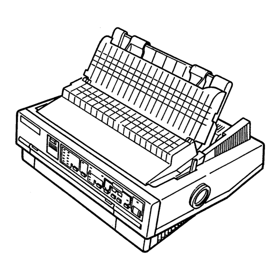
Page 4: Figure 1-1. Exterior View Of The Lq-570
REV.-A Table 1-2. Optional Units Model Description C806371(EAI ver.) I Single-bin cut sheet feeder(80-column) C806372(others) I Single-bin cut sheet feeder(80-column) C806381(EAI ver.) I High-capacity cut sheet feeder(80-column) C806382(others) I High-capacity cut sheet feeder(80-column) C800191(EAI ver.) I Tractor unit(80~lumn) C800192(others) I T r a c t o r unit(80adumn) 7753 I Fabric ribbon cartridge(80-column) 7768... -
Page 5: Specifications
REV.-A ~- 1.2 SPECIFICATIONS This section provides specifications for the LQ-570+ printer. 1.2.1 Hardware Specifications Serial, impact, dot matrix Printing method 24 wires (12x 2 staggered, diameter 0.2 mm) Pin mnfiguration Wires 2 Wires 1 Friction feed (front/top) Feeding methods Push tractor feed (rear) Pull tractor feed (fronthttom) Push-pull tractor feed (with optional tractor) (rear) -
Page 6: Table 1-3. Specifications For Cut Sheets
REV.-A Table 1-3. Specifications for Cut Sheets 148 mm to 257 mm (5.8 in. to 10.1 in.) (top insertion) Width 182 mm to 257 mm (7.2 in. to 10.1 in.) (front insertion) Length 364 mm (14.3 in.), maximum 0.065 mm to 0.14 mm (0.0025 in. to 0.0055 in.) Thickness Weight 14 lb to 24 lb (52.3 g/m’*2 to 90 g/m**2) - Page 7 REV.-A 220240 V version Rated voltage 220 to 240 VAC Input voltage range 198 to 264 VAC Rated frequency 50 to 60 Hz Input frequency 49.5 to 60.5 Hz Rated current 1.0 A Power consumption Approx. 33W(during a self-test in draft mode,10 cpi) Insulation resistance 10 megohms, minimum(at 500 between AC Iines and chassis).
-
Page 8: Firmware Specifications
REV.-A 1.2.2 Firmware Specifications (’ EPSON ESC/P 2( ESWPTM level 2: EPSON new control code for printers) Control code IBM emulation mode (European version only)”l NOTE: 1 :The European version is equipped with the IBM emulation mode, Please refer to the emulation mode specification for details. -
Page 9: Table 1-8. Printing Text Mode)
REV.-A See tables 1-8 and 1-9. Printing speed ~ printing COlumns See Table 1-8. See Table 1-10. Character matrix See Table 1-10. Character size Table 1-8. Printing Text Mode) Print Pitch Draft 17.1 1120 Invalid cpi: characters per inch Cps: characters per second letter quality 1-1o... -
Page 10: Table 1-9. Printing (Bit Image Mode)
REV.-A Table 1-9. Printing (Bit Image Mode) Pins Printing Speed Bit Image Printing Mode Density Printable Dots (dpi) (ips) Single-density 22.5 11.2 Dual-density Double-speed, dual-density 22.5 11.2 Quadrupledensity 1920 CRT graphics 11.2 CRT graphics II 15.0 Single-density 22.5 Dual-density 11.2 CRT graphios II 15.0 Tripledens”~... - Page 11 REV.-A Table Character Matrix and Character Size 1-10. (“ Printing Mode Face Matrix Character S&e Unit ESC sp Draft, 10 pitch 1.9 x 3.1 Draft, 12 pitch 9 x 2 2 1.9 x 3.1 Draft, 15 pitch ------ ------- Draft, 10 pitch, mndensed ------ .
-
Page 12: Table 1-13. Settings For Dip Switch 2 (Sw2)(Esc/P 2)
REV.-A 1.5 DIP SWITCHES AND JUMPER SETTING This section describes the DIP switch selections and jumper setting for the LQ-570+ printer. DIP Switch ESC/P mode 1.5.1 Setting for This printer is”equipped with two banks of DIP-SWITCHES and they are located on the control panel. The tablel -12 through 1-15 shows the available function settings of two DIP switches. -
Page 13: Jumper Setting
REV.-A Character *t ~ktion Tdda 1.14. Intamational . ---- ..----- —--— --—- .–. Table Country Others Europe France Germany U.K. Denmark 1 437Greek B~-SCll Sweden Ab.komp Italy Spain 1 -— When SW 1-4 is ON. - - - - . -
Page 14: Dip Switch Setting For Ibm Emulation Mode
REV.-A Switch Setting for IBM emulation mode 1.5.2 DIP (’ In the IBM emulation mode, with the DIP awitch 1-6 to ON, some other awitches are recognized by the printer in different meanings from the ESC/P 2 mode. Please refer to the emulation mode specif.=tion for details. Table 1-16. - Page 15 REV.-A 1.6.11 Printer Protection for Heavy-Duty Printing This printer has a printhead protection function to prevent it from overheating and to handle the printer when the head driver voltage drops. If head temperature exceeds its maximum value, printing automatically until the stops head temperature drops to a certain value before printing resumes.
-
Page 16: 1.7 Main Components
REV.-A 1.7 MAIN COMPONENTS The main mmponents of the LQ-570+ printer are designed for easy removal and replacement at maintenance and repair of the printer. The main composed of this printer are: 1) C107 MAIN board: the main control board; the CPU on this board controls all main functions. 2) C062 PNL board: the control panel bowd. -
Page 17: C062 Pnl Board (Control Panel Circuit Board)
REV.-A 1.7.2 C062 PNL Board (Control Panel Circuit Board) The C062 PNL board is the LQ-570+ control panel, which includes the indicator LEDs, switches, and DIP switches. Figure 1-13. (X62 PNL Board 1.7.3 C062 PSB/PSE Board (Power Supply Circuit Board) The power supply unit consists of a switching regulator circuit, which mnverts the AC line vottage to the DC voltages (for example, +35V and +5V) used by the printer. -
Page 18: Figure 1-16. Housing
REV.-A 1.7.4 Printer Meohanism (M-5J1O) The M-5J1o printer mechanism was developed specifically for use with LQ-570+ printer. The components inciude a carriige motor, carriage mechanism, paper-feed motor, paper-feed mechanism, ribbon-feed mechanism, printhead, and sensors. This printer mechanism ailows three ways of paper insertion. /“... - Page 19 CHAPTER 2 OPERATION PRINCIPLES 2.1 OVERVIEW OF PRINTER MECHANISM OPERATION ......2-1 2.1.1 Printhead Mechanism ..........2-1 2-13 2.3 CONTROL CIRCUIT OPERATION .
- Page 20 REV.-A 2.1 OVERVIEW OF PRINTER MECHANISM OPERATION This section describes the printer mechanism of the Model-5J10 printer unit and explains how the printer works. Model-5J10 has a printer mechanism that features a 24-pin impa~ dot printhead for serial printing. There are four main parts to the printer mechanism: 1) the printhead mechanism, 2) the carriage movement mechanism, 3) the paper advance mechanism, and 4) the ribbon advance mechanism.
-
Page 21: Control Circuit Operation
REV.-A 2.3 CONTROL CIRCUIT OPERATION The control circuit consists of two boards: the C107 MAIN board, which acts as the main board, and the C062 PNL board, which acts as the control panel board. This section describes how these boards work. - Page 22 REV.-A Table 2-5 lists the functions of the main components and circuits of the printer. The CPU converts the print data sent from the host mmputer to image data (the print image). The image data is then loaded ‘) to RAM. Each line of data is processed sequentially. The CPU transfera the print data to the printhead drive circuit.
- Page 23 REV.-A Table 2-5. Functions of the Main IC and Circuits (Cont.) Location Functions IC or Circuit PROM contains the program that runs the CPU. PROM IC14 IC15 Holds the CPU working area and the various buffers. (1E is not used for an 80- IC16 column device and is not installed.) MROM...
- Page 24 REV.-A Power On CpU Self Reset +6 V Line VCCOM THLD ??EStt Figure 2-20. /F?ESET Signal Timing 2.3.3 Sensor Circuits Figure 2-21 shows thesensorcircuits block diagram. Detection of any excessive printheadtemperature causes the TEMP2 signal to be sent directly to the CPU. Other signals, such as the CRHOME signal, pass through the each low path filters before reaching the CPU.
- Page 25 REV.-A Circuit 2.3.4 MOTOR, CR Drive Figure 2-22 shows the MOTOR, CR driie circuit. An open-loop, constant-current drive control is used to drive the MOTOR, CR. The motor is driven by 2-2 phase excitation and 1-2 phase excitation. 2-2 phase excitation corresponds to two 1-2 phase excitation steps. Thus, for each single step phase change of a 2-2 phase excitation motor, the carriage moves 1/120 inch.
- Page 26 REV.-A PF Drive Circuit 2.3.5 MOTOR, “) The printer uses a stepping motor to advance the paper. The paper can be advanced for minimum of 1/380 inch. The nmtor is a 2-2 phase or 1-2 phase, constant-voltage drive type. P70 to P73 on the CPU are the phase oontml ports forthe stepping motor.
- Page 27 REV.-A 2.3.6 Printhead Drive Circuit ‘\ Figure 2-24 shows the printhead drive circuit block diagram. The print data already is expanded to create the image data. The CPU splits up this data three times and transfers this information to the latch circuit within the Head Gate Array(lC2).
-
Page 28: Disassembly And Assembly
REV.-A CHAPTER 3 ‘) DISASSEMBLY AND ASSEMBLY 3.2.1 Changing the Printhead ..........3-5 3.2.3 Removing the Eleotrkal Cirouitty . - Page 29 REV.-A the Circuit Boards 3.2.1 Removing FRAME ASSY.,SHEET GUIDE. Remove Remove COVER ASSY.,EJECT. COVERASSY.,EJECT ASSY.,SHE= GUIDE Figure 3-2. Removing the FRAME ASSY., ;HEET GUIDE and the COVER ASSY., EJECT Release the two levers that hold the printhead to the oarriage, and remove the printhead. Remove the two FFCS (CABLE, HEAD, FRONT(,REAR)) from the printhead.
- Page 30 REV.-A 3.2.3 Removing the Circuit Boards This section describes how to remove the BOARD ASSY.,MAIN (C107 MAIN board), the BOARD ASSY.,POWER SUPPLY (C062 PSB/PSE board) and the BOARD ASSY.,PANEL (C062 PNL board). 3.2.3.1 Removing the BOARD ASSY.,MAIN (C107 MAIN Board) Remove the HOUSING ASSY.,UPPER (see Section 3.2.2.2).
- Page 31 REV.-A CBB(C) (M3X 10) Screws CB (M3X8)’Screw BOARD ASSY., MAIN Figure 3-7. BOARD ASSY.,MAIN Adjustment Required When replacing the BOARD ASSY.,MAIN, you must adjust the bidirectional print position again to ensure bidirectional printing is mrrectly aligned <Bidirectional Print position adjustment(See section 4.2)> Removing the BOARD ASSY.,POWER SUPPLY (C082 PSB/PSE Board) 3.2.3,2 Remove the HOUSING ASSY.,UPPER (see Section 3.2.2.2).
- Page 32 CHAPTER 4 “’) ADJUSTMENTS 4.3 CIRCUIT ADJUSTMENT ............4.3.1 Adjustment Process .
- Page 33 REV.-A 4.3 CIRCUIT ADJUSTMENT ‘) The C107 board contains variable resistor VR1, which is used for balancing the circuitry. When any of the MAIN following parts are replaced, the circuitry must be balanced by adjusting the VR1. R6, R7, TL431(IC1), and VR1 If the circuitry is not properly adjusted, the CPU A/D converter functions abnormally and causes irregular operation of the printer.
-
Page 34: Chapter 5 Troubleshooting
CHAPTER 5 TROUBLESHOOTING REPAIR BY UNIT REPLACEMENT ..........5-14 5.4 REPAIR OF THE MAIN BOARD . - Page 35 REV.-A # 2 0 # 4 0 # 8 0 o #11 it21 H 240 Wire Assignment *7 82 83 410 418 #122 ‘- Coil Resistance: 45.5 *3.2 fl at 25*C (Between each dot wire and common.] ( Terminal Assignment J Figure 5-2.
-
Page 36: Repair Of The Main Board
REV.-A 5.3 REPAIR OF THE MAIN BOARD This section provides instructions for repairing the main board when it is defective and describes variius symptoms, likely causes, and checkpoints. Checkpoints refer to proper waveforms, resistance values, and other values to be checked to evaluate the operation of any component that might be bad. - Page 37 Tabla 5-4. Ranair nf the Main Circuit Board (Continued ----- - ..- . . . -. ---- .-. —... ------- —-—- — ,— —-----–—..‘) ‘) 5-15...
- Page 38 REV.-A Table =. Rebair of the Main Circuit Board (Continued) —— ‘ ? —r—— Solutlon Problem Symptom Cause Checkpoint Iclo The carnage Carnage Replace operates operation Is defectrve Iclo abnormally unstable(lack of torque) Self-test Self-test w not The CPU can Adjust VR1 Measure the voltage at pm 59(Vref) of prmtmg...
- Page 39 REV.-A 5.5 REPAIR OF THE PRINTER ‘) For detailed procedures for replacing or adjusting parts, refer to Chapter 3, Dimssemb/yandAswmb/y, and Chapter 4, Ao@hr?ent. If a problem or symptom recurs following an attempted repair, refer to Table 5-5 to try to find other potential causes.
- Page 40 REV.-A (Continued} Tahln -K Rannir nf tha Printar Maehanism . ---- . -. . .- ~-.. -......--..-..--——, Problem Symptom Cause...
- Page 41 REV.-A TsIhla 5-!5. Ranair nf Printer Mechanism (Continued) . ---- - -- ------- -- - ------- ---- —-- —.. .— --- , ‘ 1 Checkpoint Solution Problem Symptom Cause Replace the ribbon feed is The ribbon is not The ribbon Dismount the ribbon ribbon cartridge.
- Page 42 REV.-A APPENDIX ......CONNECTOR SUMMARY ....... .
- Page 43 REV.-A A.1 CONNECTOR SUMMARY Figure A-1 illustrates the interconnection of the primary components. Table A-1 summarizes the functions and sizes of the connectors. ImF7 ‘ Model 5J-10 PRINTER MECHANISM I(COGZ PNL I I G A P L E V E R C R H O M E PE-2 PE-I CRMOTORPFMOTOR HEAD H E A D I p30ARD) I’b...
- Page 44 REV.-A Tabla A-1. Board Connector Summarv . ---- - . -. ———- — —- ----- —-— — Pins Board Funotion Conneotor ‘\ BOARD ASSY.,PANEL BOARD ASSY.,MAIN BOARD ASSY.,POWER AC power input SUPPLY DC power output BOARD ASSY.,MAIN Parallel interface (C107 MAIN BOARD) Optional interface card Control panel MOTOR,CR...
- Page 45 REV.-A Table A4. CN4 BOARD ASSY. MAIN {C107 MAIN) Table A-2 CN2 BOARD ASSY., MAIN (C107 MAINI Function No. 1/0 Signal Name Signal Name Function MOTOR, CR phase A +5 VDC MOTOR, CR phase B + 5 VDC MOTOR, CR phase C + 5 VDC MOTOR, CR phase D + 5 VDC...
- Page 46 REV.-A MAIN) Tabla A-13. CN13 BOARD ASSY. MAIN 4C107 Table A-7. CN7 BOARD ASSY. MAIN [C107 MAIN’ Function Signal Name Function Signal Name Power switch signal Head data 3 +5 VDC HD1 1 Head data 11 +5 VDC Head data 2 HD19 Head data 19 Signal ground...
- Page 47 REV.-A , A.5 CASE OUTLINE DRAWING H-II i—--- Figura A-17. LQ-570+ Case Outline Drawing A-22...
- Page 48 REV.-B — I — 00001 00001 1’ Donut — _====! Figure A-18. LQ-107O Case Outline Drawing A-23...
- Page 49 EPSON...
Need help?
Do you have a question about the LQ-570 and is the answer not in the manual?
Questions and answers