Table of Contents
Advertisement
COLOR MONITOR
SERVICE MANUAL
CHASSIS NO. : CL-82
MODEL:
(
) **Same model for Service
CAUTION
BEFORE SERVICING THE UNIT,
READ THE SAFETY PRECAUTIONS IN THIS MANUAL.
-
+
Website:http://biz.LGservice.com
E-mail:http://www.LGEservice.com/techsup.html
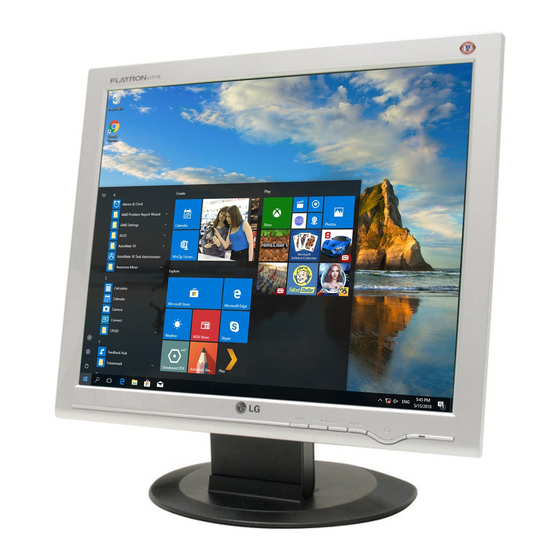
L1717S
(L1717S-SNN.AN**EP)
L1717S
(L1717S-BNN.AN**EP)
L1717S
(L1717S-GNN.AN**EP)
*To apply the MSTAR Chip.
Advertisement
Table of Contents


Need help?
Do you have a question about the L1717SBN - - 17" LCD Monitor and is the answer not in the manual?
Questions and answers