
Related Manuals for Quectel UC200A-GL


Summarization of Contents
Legal and Compliance
Legal Notices
General legal information and disclaimers.
Use and Disclosure Restrictions
Terms regarding content usage and intellectual property.
Copyright
Statement on intellectual property rights.
Trademarks
Guidelines for brand name usage.
Third-Party Rights
Mentions of third-party materials and their terms.
Disclaimer
Limitation of liability and warranty information.
Safety Information
Driving Safety
Precautions while operating vehicles.
Aircraft Safety
Rules for device use on airplanes.
Medical Equipment Interference
Warnings for hospitals.
Emergency Call Functionality
Limitations of emergency calls.
RF Interference
Potential interference with other devices.
Explosive Atmospheres
Safety in hazardous areas.
Introduction
Special Marks
Explanation of symbols used in the document.
Product Overview
Frequency Bands and Functions
Details on supported wireless networks and features.
Key Features
Summary of the module's main capabilities.
Pin Assignment
Location and numbering of module pins.
Pin Description
Detailed explanation of each pin's function.
Evaluation Board (EVB)
Information about the development hardware.
Operating Characteristics
Operating Modes
Different states of the module operation.
Sleep Mode
Power saving features and configurations.
Airplane Mode
How to disable RF functions.
Power Supply
Power input requirements and design.
Turn On Procedures
Methods for powering the module.
Turn Off Procedures
Methods for powering down the module.
Reset Functionality
How to reset the module.
Application Interfaces
USB Interface
Details on the USB connection and functions.
USB_BOOT Interface
Interface for emergency download mode.
(U)SIM Interface
Connection for SIM cards.
PCM and I2C Interface
Interfaces for audio and general communication.
UART Interface
Serial communication interfaces.
SDIO Interface
Interface for SD cards.
ADC Interface
Analog-to-Digital Converter inputs.
Indication Signals
Status and network indicators.
MAIN_RI Behavior
Functionality of the Ring Indicator pin.
RF Specifications
Cellular Network
Frequency bands and antenna interface.
Transmitting Power (Tx Power)
Output power levels.
Receiving Sensitivity (Rx Sensitivity)
Signal reception capability.
Reference Design of RF Routing
Guidelines for PCB RF trace routing.
Antenna Design Requirements
Specifications for antenna integration.
RF Connector Recommendation
Recommended connectors for antenna.
Electrical Characteristics & Reliability
Absolute Maximum Ratings
Voltage and current limits.
Power Supply Ratings
Operational voltage and current specs.
Power Consumption
Module's current draw in various modes.
Digital I/O Characteristics
Voltage levels for digital signals.
ESD Characteristics
Electrostatic Discharge sensitivity.
Operating and Storage Temperatures
Environmental limits.
Mechanical Information
Mechanical Dimensions
Physical size of the module.
Recommended Footprint
PCB layout guidelines for mounting.
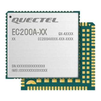
Top and Bottom Views
Visual representation of the module.
Storage, Manufacturing & Packaging
Storage Conditions
Guidelines for storing the module.
Manufacturing and Soldering
Processes for assembly.
Packaging Specifications
Details on how the module is packed.
Appendix References
Related Documents
List of supporting documentation.
Terms and Abbreviations
Glossary of technical terms.
Warnings and Compliance
OEM Installation Limitations
Restrictions on installation.
FCC Compliance and Labeling
Regulatory requirements.
Manual Information to End User
Guidelines for user manuals.
Radiation Exposure Statement
Safety information regarding RF exposure.
Need help?
Do you have a question about the UC200A-GL and is the answer not in the manual?
Questions and answers