JVC GY-DV300U Service Manual
Dv camcorder
Hide thumbs
Also See for GY-DV300U:
- Instruction manual (108 pages) ,
- User manual (42 pages) ,
- Using manual (8 pages)
Advertisement
Quick Links
SERVICE MANUAL
DV CAMCORDER
GY-DV300U/UZ/E
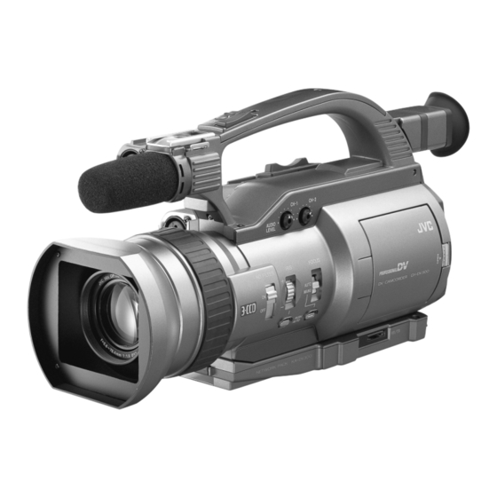
The photo shows the GY-DV300 DV camcorder with an optional KA-DV300 network pack.
Differences between GY-DV300U and GY-DV300UZ are packed accessories.
For more details, refer to the "SECTION 7 PACKING" on page 7-1.
No. 60139
March 2002
100% recycled paper
COPYRIGHT © 2002 VICTOR COMPANY OF JAPAN, LTD.
Advertisement

Related Manuals for JVC GY-DV300U


Summary of Contents for JVC GY-DV300U
- Page 1 DV CAMCORDER GY-DV300U/UZ/E The photo shows the GY-DV300 DV camcorder with an optional KA-DV300 network pack. Differences between GY-DV300U and GY-DV300UZ are packed accessories. For more details, refer to the ”SECTION 7 PACKING“ on page 7-1. No. 60139 March 2002 100% recycled paper COPYRIGHT ©...
- Page 2 Important Safety Precautions Prior to shipment from the factory, JVC products are strictly inspected to conform with the recognized product safety and electrical codes of the countries in which they are to be sold. However, in order to maintain such compliance, it is equally important to implement the following precautions when a set is being serviced.
- Page 3 Safety Check after Servicing Examine the area surrounding the repaired location for damage or deterioration. Observe that screws, parts and wires have been returned to original positions, Afterwards, perform the following tests and confirm the specified values in order to verify compli- ance with safety standards.
- Page 4 SECTION 1 SERVICE CAUTIONS AND DISASSEMBLY REMOVAL OF THE EXTERNAL COVER 1.1.2 Removing the right side cover (1) Remove the two screws from the right side. 1.1.1 Removing the left side cover (1) Slide the EJECT switch in the direction of the arrow and open the cassette cover in the direction shown.
- Page 5 1.1.3 Removing the handle assembly 1.1.4 Removing the rear panel (1) Remove the left and right side covers as described in “1.1.1 (1) Remove the left and right side covers as described in “1.1.1 Removing the left side cover” and “1.1.2 Removing the right Removing the left side cover”...
- Page 6 (4) Removing the rear panel exposes the REG. board. BOARD LAYOUT Caution Take measures against static when handling the circuit board. The ICs mounted on the circuit board (especially the IC402, which is the CPU on the main circuit board) may be damaged by static.
- Page 7 REMOVAL OF THE LENS AND OPTICAL COMPONENTS (3) Remove the right side cover as described in “1.1.2 Remov- ing the right side cover.” 1.3.1 Removing the lens hood (4) Remove the two screws and the manual iris control dial (1) In order to remove the lens hood on the front of the main assembly.
- Page 8 (7) After removing the three screws from the CCD block DISASSEMBLY OF MICROPHONE ASSEMBLY assembly on the rear part of the lens assembly, the CCD (1) Remove the handle as described in “1.1.4 Removing the block assembly can be removed from the lens. handle assembly.”...
- Page 9 REMOVAL OF THE VIEWFINDER REMOVAL OF THE LCD MONITOR (1) Pull up the viewfinder and remove the two screws from (1) Remove the right side cover as described in “1.1.2 Remov- the stay. ing the right side cover. (2) Remove the two screws which are inside the right side cover.
- Page 10 REMOVAL OF THE MECHANISM ASSEMBLY (5) Disconnect the wires from CN5508, CN5501 and CN5506 of the DV MDA board, and then remove the mechanism (1) Remove both the left side and right side covers from the assembly. main unit. (See “1.1.1 Removing the left side cover” and DV MDA board “1.1.2 Removing the right side cover.”) ⁄...
- Page 11 HOW TO TAKE OUT THE CASSETTE TAPE IN AN SERVICE MENUS EMERGENCY 1.9.1 Modes required in servicing When the cassette tape cannot be ejected due to a failure in (1) Characters are displayed on the LCD monitor screen or view- the electrical circuitry, take out the cassette manually as de- finder.
- Page 12 1.9.2 Operation in the first-level of the service menu (2) Rotate the SELECT dial to move the cursor (') on the mode to be modified. (1) While holding down the specified button(s) (PLAY, STOP), (3) Push the SELECT dial so that the parameter blinks. press and hold the MENU button for more than 1 second.
- Page 13 • When the white blemish detection completes, the result data Details on correctable white blemish is stored in the memory of the CPU, “ERROR DETECT END, • Up to 32 errors with composite video levels of 50 mV or PLEASE POWER OFF” is displayed. Turn the POWER switch more can be corrected.
- Page 14 1.9.5 VTR1 menu Operating Procedure (1) Rotate the SELECT dial to move the cursor onto the item to be changed. – – – V T R 1 – – – (2) Push the SELECT dial so that the parameter value blinks. T .
- Page 15 1.9.6 VTR2 menu – – – V T R 2 – – – S E N S O R 1 0 9 P ( D E W ) C L O G L E V E L C L O G L E V E L B A C K Fig.
- Page 16 1.9.8 DIP SW menus These menus set the DIP switches. (The factory setups are all “OFF”, or “0”.) – – – D I P S W 1 / 3 – – – – – – D I P S W 2 / 3 –...
- Page 17 1.9.9 HOUR METER menu – – – H O U R M E T E R – – – This menu is used to clear hour meters. : C L E A R D R U M : 0 0 0 0 0 0 Set the desired parameter to “CLEAR”...
- Page 18 (1) Bytes 1, 2: Error code On-Screen Display Code Cause Warning Content & Detection Method VTR WARNING [DEW] Dew condensation Detection of voltage at MAIN board IC3 pin 100. DEW ON : 2.4V DC or more DEW OFF: 1.8V DC or less VTR WARNING [HARD] Loading motor, rotary Loading does not complete.
- Page 19 (2) Byte 5: Mechanism position at error occurrence CASSETTE-IN LOAD FAST CASIN2HALF LOAD2FWD REV2STOP INVALID HALF STOP INITIAL HALF2LOAD FWD2REV STOP2FAST Table 1-9-10 (2) Mechanism Position (3) Bytes 6, 7: VCR mode. (4) Bytes 8, 9: Key code Code VTR Mode Code Key Code Code...
- Page 20 1.9.11 OTHERS menu – – – O T H E R S – – – O R Y L O A D : O F F O R Y S W S A V E : O F F R E S E T : C A N C E L .
- Page 21 1.10 EEPROMS (1) EEPROMs and stored data EEPROM Board Name Memory Contents IC406 A/L/S board Menu setting data Camera adjustment data DVC adjustment data IEEE1394 ID data HOUR METER data ERROR HISTORY IC907 MAIN board Lens adjustment data After replacement of a board or EEPROM, the EEPROM contains no data at all. But it is initialized automatically when the power is turned on.
- Page 22 SECTION 2 MECHANICAL ADJUSTMENTS 3) 80-minute tape BEFORE ADJUSTMENTS If an 80-minute tape is used, block noise may occur during 2.1.1 Precautions playback even when playing a tape that has been recorded using the same unit. Therefore 80-minute tapes cannot 1) Be sure to apply a screw securing torque when attaching a be used.
- Page 23 BASICS OF MECHANISM DISASSAMBLY/ASSEMBLY 2.2.1 Assembly mode The disassembly and assembly of the mechanism can be done SEMBLY mode, apply 3 V DC to the electrodes at the top of the in the ASSEMBLY mode (see Table 2-2-1). loading motor shown in Fig. 2-2-1. The ASSEMBLY mode is set The ASSEMBLY mode is provided in the intermediate position when the markings (red) on two gear teeth of the rotary en- between C-IN and S.FF.
- Page 24 2.2.2 Mechanism modes The mechanism has 6 modes as shown in Table 2-3-1. The current mode can be confirmed by observing the markings on the sub-cam gear and the 8 mark on the main deck at the back side of mechanism assembly. See Figs. 2-2-2 to -7. 1.
- Page 25 MECHANISM TIMING CHART See following table (Table 2-3-1). MODE ASSEMBLY LOADING END C-IN S. FF PLAY STOP FF/REW PARTS ROTARY ENCORDER ROTARY ENCODER 33.33 166.66 193.33 226.66 273.33 306.66 MAIN CAM GEAR SUB CAM GEAR POLE BASE S/REV PLAY CTL PLATE FF/REW ON 1 MAIN BRAKET(SUP)
- Page 26 MAINTENANCE AND INSPECTION OF MAJOR PARTS Periodical inspection and maintenance are requisite to maintain the product will not only reduce considerably but other the initial performance and reliability of the product. Table 2-4-1 unfavorable influences may produce. (Maintenance & Inspection List) has been compiled assuming Rubber parts may deform or degrade after long period of stor- standard operating conditions, and the specifications in the ta- age even if they are not used in this period.
- Page 27 2.4.2 Maintenance and inspection list 1) The 6000 H maintenance consists of a replacement of the entire mechanism assembly. 2) When mounting the capstan motor on the main deck, control of the verticality is required. Therefore, when the capstan motor reaches the end of its service life, the entire mechanism assembly should be replaced.
- Page 28 2.4.3 Cleaning Upper drum High-quality paper The mechanism incorporates a video head cleaner that is effec- Head tip tive for the removal of magnetic dust, etc. However, tape lubri- cant adhering to the head surface produces a spacing loss, it is recommended to polish the heads using a head cleaning tape.
- Page 29 PERIODICAL MAINTENANCE Perform maintenance at the correct times in accordance with the maintenance table. Fig. 2-5-1 shows the flow chart of periodical maintenance procedures at different operating hours. 2000-hour maintenance 6000-hour maintenance Start Start Replaced parts Replaced parts Mechanism assembly ⁄...
- Page 30 DISASSEMBLY/ASSEMBLY OF MECHANISM ASSEMBLY 2.6.2 Screws and washers used in mechanism assembly disassembly/assembly 2.6.1 Assembly/disassembly The following table shows the mechanism assembly/disassem- Table 2-6-1 shows the symbols, designs, part numbers and colors bly procedures. of the screws and washers used with the Mechanism assem- : Names of the disassembled/assembled parts.
- Page 31 2.6.3 Mechanism assembly disassembly procedure table Part Name Item No. Points Remark Å Cassette housing assembly 2 (S2), 2(S4) Drum assembly 3 (S2) Motor bracket assembly 4 (S2) Middle catcher assembly 3 (S2) Reel cover assembly (S2), 2 (L6) Pinch roller arm assembly (W1), (L7) Sub-brake assembly (P1), (W1), (L8)
- Page 32 ∼ ∼ Fig. 2-6-1 2.6.4 Mechanism disassembly/assembly procedure chart <How to read the chart> ⋅ The following chart shows the disassembly/assembly procedures by dividing them into blocks A to I. ⋅ To remove the tension arm sub-assembly which is located in block D; start disassembly from block A. The tension arm sub-assembly can be removed as the fourth operation after the removals of the cassette housing assembly (block A) →...
- Page 33 Item Reference picture/drawing Procedure REPLACEMENT OF MAJOR PARTS ⋅ Make sure that the mechanism is in the ASSEMBLY mode before proceeding to disassembly or assembly. (See section 2.1, “Assembly Mode”.) ⋅ Screws must always be tightened using a torque screwdriver and at the specified torque. Å...
- Page 34 Item Reference picture/drawing Procedure Pinch roller arm assembly <Removal> 1) Remove the washer (W1) and pull out the assem- ( W1 ) bly. <Attaching> Å 1) Fit the pinch roller arm assembly into the boss (L7) of the charge arm assembly. 2) Attach the washer (W1).
- Page 35 Item Reference picture/drawing Procedure Middle catcher assembly <Removal> 1) Remove the 3 screws (S2) and remove the assem- bly. ( S2 ) 11 ( S2 ) ( S2 ) <Attaching> 1) Reverse the removal procedure. Fig. 2-7-5 Reel cover assembly <Removal>...
- Page 36 Item Reference picture/drawing Procedure Swing arm assembly <Removal> 1) Pull the assembly upward. <Attaching> 1) Reverse the removal procedure. Fig. 2-7-7 2-15...
- Page 37 Item Reference picture/drawing Procedure Band arm plate assembly, Tension arm assembly <Removal> 1) Remove the washer (W2). ( S3 ) 2) Remove the screw (S3). ( W2 ) 3) Remove the spring (P2). 4) Remove the band arm plate assembly and tension arm assembly.
- Page 38 Item Reference picture/drawing Procedure <Tension arm assembly position adjustment> 1) Without loading a tape, set the mechanism mode to PLAY mode. To switch the mode, rotate worm wheel 2 while the motor bracket assembly is disengaged (see 2.2, “Mechanism Modes”). 2) Rotate the tension arm slightly clockwise to elimi- nate production of rattle with the band arm plate.
- Page 39 Item Reference picture/drawing Procedure Sub-deck assembly <Removal> 1) Remove the 5 screws (S2) and pull out the assem- bly. ( S2 ) ( S2 ) ( S2 ) ( S2 ) ( S2 ) <Attaching> 1) While sliding the control plate toward the left, at- tach the sub-deck assembly.
- Page 40 Item Reference picture/drawing Procedure Reel base (SUP) assembly, Reel base (TU) assembly, <Removal> & Control plate, Prism 1) Pull up each assembly to remove it. The control plate can be removed by sliding it toward the left as shown by the arrow. 2) Remove the screw (S2) to remove the prism.
- Page 41 Item Reference picture/drawing Procedure Base plate assembly <Removal> 1) Remove the screw (S2) and take out the assem- bly. ( S2 ) <Attaching> 1) Attach the assembly to the boss (L14) as if insert- ing, then clamp with the screw. ( L14 ) Fig.
- Page 42 Item Reference picture/drawing Procedure fi fl ‡ Reel drive pulley assembly, Push plate, Clutch lock gear 1, <Removal> ° Clutch lock gear 2, R. drive gear 1, R. drive gear 2 1) Remove the washer (W1) and take out the assem- bly.
- Page 43 Item Reference picture/drawing Procedure · ‚ Tension control arm assembly, Brake control arm assembly, <Removal> ¡ Charge arm assembly 1) The brake control assembly can be removed after removing the washer (W1). ( L16 ) ( W1 ) <Attaching> 1) Align the phases of the main cam and sub cam , then attach by reversing the removal procedure.
- Page 44 Item Reference picture/drawing Procedure ™ £ Connect gear 2 (SUP), Connect gear 2 (TU) <Removal> 1) Remove the screw (S2) and take out the gears. ( S2 ) <Attaching> 1) Reverse the removal procedure. The two connect gears 2 are given the same part number. ( S2 ) NOTE ⋅...
- Page 45 Item Reference picture/drawing Procedure ¢ ∞ § Rotary encoder assembly, Main cam , Arm gear 1 assembly, <Removal> ¶ Centering arm assembly 1) The rotary encoder can be removed by removing the 2 screws (S2). 2) The main cam can be removed by removing the ( S2 ) washer (W1).
- Page 46 Item Reference picture/drawing Procedure • ª º Sub cam Arm gear 2 assembly, Clutch lock lever assembly <Removal> 1) Remove the screw (S2) and take out the sub cam . As L19 is engaged at the rear of the main deck assembly while the phase is aligned, deviate the phase in the direction of the arrow before removal.
- Page 47 CONFIRMATION AND ADJUSTMENT OF MECHANISM PHASES See Fig. 2-8-1. 22 Worm wheel 2 36 Arm gear 1 assembly See section 2.7.14 See section 2.7.18 34 Rotary encorder assembly See section 2.7.18 39 Arm gear 2 assembly See section 2.7.19 38 Sub cam See section 2.7.19 35 Main cam 37 Centering arm assembly...
- Page 48 DISASSEMBLY PROCEDURE LIST 14(S3) (W2) (S2) (S2) (S2) (S2) (P3) (W1) 6(S2) 9(S2) (S2) 7(S2) 8(S2) (S2) (S2) (S2) (S2) (S2) (S2) (S2) (S2) (S2) (S2) 31(S2) (S2) (S2) (S2) (S2) (S2) (W1) (S2) (S2) (W1) (S2) (W1) (S2) ADJ. (W1) (P7) (S2)
- Page 49 2.10 MECHANISM DISASSEMBLY/ASSEMBLY SHEET Screw Management Å Drawing No. Table Application Ref. No. No.1 No.2 No.5 No.8 No.9 Å Cassette housing assembly Drum assembly Reel cover assembly ( S2 ) ( S2 ) ( S2 ) ( S2 ) S2 × 3 S2,L6 ×...
- Page 50 Screw Management ( ) ⁄ ™ £ ¢ • 19 20 21 22 23 24 25 26 27 28 29 30 31 32 33 34 S2 S2 S2 S2 S2 S2 S2 S2 S2 S2 S2 S2 S2 S2 S2 S2 The slit washers cannot be reused once they have been removed.
- Page 51 2.11 TORQUE ADJUSTMENTS Measuring point ( * ) Measuring Adjustment parts ( - ) Item instruments & Mode Adjustment procedure Adjustment level ( + ) Input signals * Supply side indica SUP backup • Cassette torque Play (1) Insert the cassette torque meter and enter play torque meter tion of cassette...
- Page 52 2.12 COMPATIBILITY ADJUSTMENT 2.12.1 Compatibility adjustment flow chart Fig. 2-12-1 shows the flow chart of compatibility adjustment. Start Connect the connector board. Enter modes PLAY → SEARCH REV → Set the RF envelope adjusted waveform flat. SEARCH FWD → PLAY in this sequence, and ensure that tape is not damaged by wrinkles.
- Page 53 2.12.2 Tape transport restriction TU guide roller MID guide roller The unit uses only the SUP guide roller and TU guide roller to SUP slant pole restrict the tape transport. The tape is free (no restriction) from SP guide roller other parts.
- Page 54 Measuring point ( * ) Measuring Adjustment parts ( - ) Item instruments & Mode Adjustment procedure Adjustment level ( + ) Input signals 2.12.3 Compatibility adjustment Preparation (1) Mount a connector board to the CN23 on the A/L/S board by inserting it in the slot that is provided to accommodate it.
- Page 55 Measuring point ( * ) Measuring Adjustment parts ( - ) Item instruments & Mode Adjustment procedure Adjustment level ( + ) Input signals Eject →Play * TP9 ENV OUT (1) Switch the mode from Eject → Play and en- Waveform •...
- Page 56 SECTION 3 ELECTRICAL ADJUSTMENTS 3.1 REQUIRED MEASURING INSTRUMENTS AND STANDARD SETUP FOR ADJUSTMENT 3.1.1 Test instruments required for adjustment Instrument Condition Instrument Condition Oscilloscope Capable of measuring 100 MHz or higher Frequency counter Readable in 8 or more digits and calibrated. bands and calibrated.
- Page 57 3.2 STANDARD SETUP Color monitor Waveform monitor (WFM) Oscilloscope Vectorscope 75 Ø terminator 75 Ø terminator Test pattern CH-1 CH-2 AUDIO 2 m or more LEVEL ND FILTER IRIS FOCUS AUTO MANU DV CAMCORDER GY-DV300 PUSH AUTO AC adapter (7.2 V DC input) 3200K GY-DV300 lighting...
- Page 58 Procedure (1) Enter the CAM-A mode and, while holding the FF and REW buttons, turn the power ON. (2) When the power is ON, press the MENU button to display the ADJUST MENU. (3) Push the SELECT dial button so that “*” blinks, and rotate the SELECT dial to the specified value while observing the designated TP and measuring instrument.
- Page 59 Color bar Vectorscope and justment data in memory. output the burst level should as specified. • 0.286 ±0.015 Vp-p (GY-DV300U) • 0.3 ±0.015 Vp-p (GY-DV300E) * VIDEO OUT SETUP OFF • Oscilloscope ADJUST (1) Select ADJUST MENU No. 3, “SETUP OFF”.
- Page 60 (7) Select ADJUST MENU No. 6, “MASTER + 53 ±7 mVp-p MENU BLACK”. No. 6: MAS- (GY-DV300U) (8) Push the SELECT dial button so that “*” blinks, TER BLACK and then rotate the SELECT dial to adjust to + 0 ±7 mVp-p the specified value.
- Page 61 Measuring point (*) Measuring Adjustment parts (-) Item instruments & Mode Adjustment procedure Input signals Adjustment level (+) 3.4.4 Video white level adjustments * VIDEO OUT IN GAIN • Oscilloscope ADJUST (1) Select ADJUST MENU No. 7, “IN GAIN (G)”. - SELECT dial adjustment or WFM...
- Page 62 (13) Adjust the IRIS adjustment dial of the lens so + 110 mVp-p that the white peak level of the gray scale is (GY-DV300U) 100% (Gch Ref DATA display: “130”). + 55 mVp-p (14) Adjust the SELECT dial to the specified value.
- Page 63 Measuring point (*) Measuring Adjustment parts (-) Item instruments & Mode Adjustment procedure Input signals Adjustment level (+) 3.4.6 LENS adjustment * VIDEO OUT LENS HOLE ADJUST (1) Select ADJUST MENU No. 13, “LENS HOLD - SELECT dial MENU AMP”. + Automatic adjustment No.
- Page 64 Measuring point (*) Measuring Item instruments & Mode Adjustment parts (-) Adjustment procedure Input signals Adjustment level (+) 3.4.7 MONITOR LCD adjustment * For the MONITOR LCD adjustment, the following adjustments are required only. * TL312 and TL313 of WHITE •...
- Page 65 Measuring point (*) Measuring Adjustment parts (-) Item instruments & Mode Adjustment procedure Input signals Adjustment level (+) * TL311 and TL313 of ADJUST (6) Select ADJUST MENU No. 44, “LED SUB- MENU ALS PWB ASSY CONTRAST B”. - SELECT dial No.
- Page 66 Measuring point (*) Measuring Item instruments & Mode Adjustment parts (-) Adjustment procedure Input signals Adjustment level (+) * MONITOR LCD H-POSITION • Grey scale chart ADJUST (1) Set ADJUST MENU No. 52, “LCD H-POSI- - SELECT dial adjustment (Just scan) MENU TION”.
- Page 67 Measuring point (*) Measuring Adjustment parts (-) Item instruments & Mode Adjustment procedure Input signals Adjustment level (+) * TL322 and TL323 of WHITE • Oscilloscope ADJUST • Proceed to the following this adjustment af- BALANCE • Gray scale chart MENU ALS PWB ASSY ter having completed the adjustment of cam-...
- Page 68 Measuring point (*) Measuring Item instruments & Mode Adjustment parts (-) Adjustment procedure Input signals Adjustment level (+) * VF LCD H-POSITION • Grey scale chart ADJUST (1) Select ADJUST MENU No. 63, “VF H-POSI- - SELECT dial adjustment (Just scan) MENU TION”.
- Page 69 Measuring point (*) Measuring Adjustment parts (-) Item instruments & Mode Adjustment procedure Input signals Adjustment level (+) 3.5 ADJUSTMENTS OF THE DVC BLOCK Mount a connector board to the CN23 on the A/L/S board by inserting it in the slot that is provided to accommodate it. This may be achieved without removing the R.
- Page 70 Measuring point (*) Measuring Item instruments & Mode Adjustment parts (-) Adjustment procedure Input signals Adjustment level (+) * LCD monitor SP VCO Recording tape Self REC/ (Notes) • Be sure to use a brand-new tape for - SELECT dial center (DV60 ME tape) PLAY...
- Page 71 Measuring point (*) Measuring Adjustment parts (-) Item instruments & Mode Adjustment procedure Input signals Adjustment level (+) * TP4 (FS PLL) FS PLL 48 kHz No input. (1) Select ADJUST MENU No. 110, “FS PLL 48 adjustment MODE SW: VTR ADJUST GND: TP1 (GND) kHz”.
- Page 72 3.6 REWRITE SCHEMATIC DIAGRAM Initial Pin No. Initial Parameters ON: Enable to rewrite CAM CPU ON: Enable to rewrite SYS CPU ON: Enable to rewrite LENS CPU ON: Enable to rewrite MSD CPU Not used OFF: Only factory use 3-17...
- Page 73 VICTOR COMPANY OF JAPAN, LIMITED Printed in Japan...
- Page 74 SECTION 4 CHARTS AND DIAGRAMS SCHEMATIC DIAGRAM NOTES • Wiring of connector • Schematic safety precaution ! Parts are safety related parts. (Example) When replacing them, be sure to use the specified parts. DV MDA • Voltage and waveform measurements CN5506 Voltage: Measured with digital voltmeter in DC range;...
- Page 75 REPLACING SURFACE MOUNT “CHIP” COMPONENTS [2] Chip transistors and chip F.E.T.s • Some resistors, shorting jumpers (0 resistance), ceramic capacitors, transistors, and diodes are chip parts. These chip parts cannot be reused after they are once removed. • Chip resistors used in some circuits are of high precision type having little error in resistance.
- Page 76 BOARD LOCATIONS 0 2 MAIN 0 3 A/L/S 0 6 REG 1 4 P ON 2 2 LOCK 1 2 TALLY 0 5 INPUT1 1 9 EJECT2 1 3 CONNECT 0 9 ZOOM 0 1 IS 0 6 REG 1 5 JOG 2 1 TEMP 2 0 IRIS 0 7 SWR...
- Page 77 OVERALL WIRING GIAGRAM For servicing Page 4-31 Page 4-32 DV MDA Page 4-34 Page 4-36 Page 4-24 S1 1 A/L/S P ON DGND 2.2k Page 4-20 to 4-23 Page 4-36 QSW0603-001 Page 4-5 to 4-15 JOG A JOG B JOG SW DGND CN20 TRIG LENS...
- Page 78 1/11 ( PRE/REC ) MAIN BOARD SCHEMATIC DIAGRAM FROM/TO ROTALY TRANS OF DRUM ASSEMBLY SC92711-1...
- Page 79 2/11 ( MSD ) MAIN BOARD SCHEMATIC DIAGRAM FROM/TO DV MECHANISM DV MDA ASSEMBLY CN5506 Page 4-34 OPEN TO DEW SENSOR MSD CPU PLSC1404 SC92711-2...
- Page 80 3/11 ( DV MAIN ) MAIN BOARD SCHEMATIC DIAGRAM Pg 4, 6, 8, 10, 11 MM1572FN-X OPEN OPEN OPEN SC92711-3 C75 OPEN OPEN DTC144EU-X OPEN...
- Page 81 4/11 ( CAM CPU ) MAIN BOARD SCHEMATIC DIAGRAM NETWORK PACK IC424 SN74AHC1G14K SN74AHC2G241U IC427 SN74AHC2G74U IC423 SN74AHC1G14K IC402 PLSC1402 SC92711-4...
- Page 82 5/11 ( AFE ) MAIN BOARD SCHEMATIC DIAGRAM IS CN1 Page 4-28 CN501 MM1612JN-X Cont Noise (TOP VIEW) Block diagram Bias Cont SC92711-5 Current Reference Driver limiter Thermal shutdown Noise...
- Page 83 6/11 ( PLD ) MAIN BOARD SCHEMATIC DIAGRAM Factory Use Only IC562 IC566 SN74AHC245DGV C592 R758 R765 OPEN IC565 SN74AHC245DGV RA563 NRZ0015-331 RA562 NRZ0015-331 RA561 NRZ0015-331 SC92711-6 4-10 4-10...
- Page 84 7/11 ( DBE ) MAIN BOARD SCHEMATIC DIAGRAM C616 C617 1/16 1/16 C669 C670 C626 1/16 R656 ANALOG VIDEO SC92711-7 4-11 4-11...
- Page 85 8/11 ( AF/LENS ) MAIN BOARD SCHEMATIC DIAGRAM IC905 C993 SC92711-8 4-12 4-12...
- Page 86 9/11 ( LENS DRV ) MAIN BOARD SCHEMATIC DIAGRAM LENS CONNECTOR C981 0.022 C932 0.022 SC92711-9 4-13 4-13...
- Page 87 10/11 ( LENS DRV ) MAIN BOARD SCHEMATIC DIAGRAM C980 4.7/16 SC92711-10 4-14 4-14...
- Page 88 11/11 ( CONN. ) MAIN BOARD SCHEMATIC DIAGRAM FROM/TO FROM/TO OPTIONAL CONNECT A/L/S CN8 , Page 4-23 NETWORK PACK : KA-DV300 CN9 Page 4-31 REG CN6 Page 4-32 CASS SW2 REG CN7 Page 4-32 Pg 3 , 4 , 6 , 8 , 10 , 11 Pg 3 , 4 , 6 , 8 , 10 , 11 SC92711-11 4-15...
- Page 89 MAIN CIRCUIT BOARD SIDE A A-4A IC502 B-3B IC701 B-4C Q901 B-1C A-4A A-6B A-5A R111 B-5A R134 A-5B R178 B-5A R201 A-5B R467 B-5D R517 B-4B R540 B-3A R564 B-4C R591 A-3B R615 A-4B R638 B-6C R674 A-2C R697 A-5B R765 B-3B...
- Page 90 SIDE B A-4B A-4A B-6A B-5B B-5B C120 B-5B C446 B-5D C514 B-2C C537 B-2B C560 B-3C C583 B-3C C607 B-4A C630 B-5C C653 B-5C C678 A-4C C702 B-4C C906 B-3D C929 A-2D C954 B-2D C977 B-4D A-5B K561 B-4C B-5A RA567 A-3B...
- Page 91 INNER PATTERN ( SIDE A ) 4-18 4-18...
- Page 92 INNER PATTERN ( SIDE B ) 4-19 4-19...
- Page 93 A/L/S BOARD SCHEMATIC DIAGRAM Q305 2SC4626/BC/-X M RELAY CN303 Q303 Page 4-37 2SA1790/BC/-X Q316 2SA1790/BC/-X 22/10 OS C326 22/10 C348~C351 22/10 L302 L303 SC92712-1 4-20 4-20...
- Page 94 A/L/S BOARD SCHEMATIC DIAGRAM TO MIC INPUT CN12 -6.9 Page 4-36 -6.9 CONNECT -0.3 CN12, Page 4-31 -6.9 -6.9 11.9 11.8 46.5 46.8 45.5 44.5 44.4 -0.4 11.9 11.8 46.3 46.8 45.5 44.5 44.4 -3.8 TO SPEAKER -4.0 -6.9 R824 OPEN D706 R823...
- Page 95 RN5VD26AA-X A/L/S BOARD SCHEMATIC DIAGRAM Block diagram 1 OUT Vref 3 GND TOP ZOOM CN19 Page 4-36 Pin descriptions Pin Description Number Name Output terminal Power supply terminal Ground terminal LOCK CN32 Not connect Page 4-4 External capacitor connecting terminal for delay EJECT1/ EJECT2 Page 4-4...
- Page 96 A/L/S BOARD SCHEMATIC DIAGRAM FROM/TO MAIN CN8 REWRITE : For Servicing Page 4-15 IRIS CN21 Page 4-4 SC92712-4 4-23 4-23...
- Page 97 A/L/S CIRCUIT BOARD ADDRESS TABLE OF BOARD PARTS SIDE A Each address may have an address error by one interval. A-1C Side Y axis X axis IC301 A-3B R305 B-3B R445 B-5B R730 A-2D R822 A-5D IC302 A-3A R306 B-3B R446 B-5B R731...
- Page 98 SIDE B C310 B-3B C460 B-4B C814 A-5C TP403 A-6B C311 B-3B C461 B-5A C815 A-5C TP404 A-6B C312 A-3B C462 B-4B C816 A-5C TP405 A-6B C313 B-3B C464 B-5B C817 A-4C TP406 A-6A C314 B-3B C465 B-5B C818 A-5D TP407 A-6A C315...
- Page 99 INNER PATTERN ( SIDE A ) 4-26 4-26...
- Page 100 INNER PATTERN ( SIDE B ) 4-27 4-27...
- Page 101 IS BOARD SCHEMATIC DIAGRAM 14.8 -6.6 -6.6 -0.9 -0.2 MAIN CN501 Page 4-9 14.8 14.3 14.8 -0.2 -0.7 -6.6 -6.6 -0.2 -0.7 -6.6 -6.6 -7.0 14.8 -0.2 -0.7 -6.6 -6.6 0.67Vp-p H-rate This waveform is measured as following setting. Setting the lens iris to become the Gch Ref data display is "130".
- Page 102 IS CIRCUIT BOARD SIDE A SIDE B 4-29 4-29...
- Page 103 INNER PATTERN SIDE A INNER PATTERN SIDE B 4-30 4-30...
- Page 104 CONNECT BOARD SCHEMATIC DIAGRAM AND CIRCUIT BOARD SIDE A A/L/S CN12 Page 4-21 SHORT ( 0 ) SHORT ( 0 ) MAIN CN9 Page 4-15 SIDE B R12 0 1.0Vp-p R13 0 H-rate R14 0 AGND SC93561 4-31 4-31...
- Page 105 4.10 REG BOARD SCHEMATIC DIAGRAM 6.6 2.5 1.1 1.5 1.6 4.1 1.1 1.1 1.4 1.6 1.4 2.4 DV MDA CN5508 Page 4-34 DC/BATT. IN DV MDA CN5501 15.5 Page 4-34 14.8 11.8 15.5 15.3 MAIN CN7 Page 4-15 14.7 -7.0 46.7 14.7 11.8...
- Page 106 4.11 REG CIRCUIT BOARD SIDE A SIDE B B-1B B-3C A-2D B-3B B-2B B-3C B-3A R104 B-1B R120 B-1B R152 B-1C B-3B B-2B A-3A B-1C C102 B-2C A-3B A-3C CN27 A-3B B-3B B-3C B-3C B-3B B-2B B-3B B-3A R105 B-2B R121 B-1B R153...
- Page 107 4.12 DV MDA BOARD SCHEMATIC DIAGRAM CAPSTAN MOTOR REG CN28 Page 4-32 REG CN29 Page 4-32 ROTARY ENCORDER DRUM MAIN CN2 Page 4-6 HOUSING SL92279 4-34 4-34...
- Page 108 4.13 DV MDA CIRCUIT BOARD SIDE A ADDRESS TABLE OF BOARD PARTS Each address may have an address error by one interval. A-1C Side Y axis X axis IC5501 A-4B R5529 B-3B C5523 A-4B B5501 B-2B IC5502 A-5A R5535 B-4B C5524 A-3B B5502...
- Page 109 4.14 / TOP ZOOM / INPUT1 BOARD SCHEMATIC DIAGRAM TOP ZOOM P ON CN24 Page 4-4 A/L/S CN11 Page 4-22 TALLY CN1 A/L/S CN19 Page 4-4 Page 4-22 SC94319 JOG CN25 Page 4-4 REC TRG CN26 Page 4-4 CN20 ZOOM CN20 Page 4-4 INPUT1 A/L/S CN12...
- Page 110 4.15 M RELAY / MONITOR BL BOARD SCHEMATIC DIAGRAM M RELAY MONITOR BL T901 L908 NQS0037-001X Q907~909 2SC4626/BC/-X Q911 , 912 MONITOR 2SD874/QR/-X A/L/S CN303 Page 4-20 SC93564 SC93563 4-37 4-37...
- Page 111 4.16 SWR/ TOP ZOOM/ M RELAY/ TALLY/ P ON CIRCUIT BOARD M RELAY SIDE A SIDE B SIDE A SIDE B TALLY SIDE A SIDE B P ON TOP ZOOM SIDE A SIDE B SIDE A SIDE B 4-38 4-38...
- Page 112 4.17 MONITOR BL/ FOCUS/ EJECT1/ LOCK/ ZOOM CIRCUIT BOARDS MONITOR BL EJECT1 SIDE A SIDE A SC82674-05-001 LOCK SIDE A FOCUS SIDE A SC82680-001 ZOOM SIDE A SC82672-05-001 SC82672-04-002 4-39...
- Page 113 4.18 JOG/ REC TRG/ INPUT1/ EJECT2/ IRIS/ TEMP CIRCUIT BOARDS EJECT2 SIDE A SIDE A SC82674-03-002 SC82674-06-001 REC TRG IRIS SIDE A SIDE A SC82674-04-001 INPUT1 TEMP SIDE A SIDE A SC82674-08-002 4-40...
- Page 114 SECTION 5 EXPLODED VIEW AND PARTS LIST SAFETY PRECATION Parts identified by the ! symbol are critical for safety. Replace only with specified parts numbers. NOTE Parts not denoted by parts numbers are not supplied by JVC.
- Page 115 5.1 CHASSIS ASSEMBLY M 1 View in the direction of arrow B View in the View in the direction of the arrow G View in the direction of the arrow D Note) direction of arrow I Attach the board of Note) Insert the CN12 Attach it after the focus the lens to the boss.
- Page 116 CHASSIS ASSEMBLY PARTS LIST M 1 M 1 M M ` ` ` ` Symbol Symbol Part No. Part Name Description Part No. Part Name Description 1 LW20079-001B HOOD COVER 57 LL40340-001B SWITCH BRACKET 2 LW20078-002A-H LENS HOOD 58 SCV2803-0614B LOCK -ALS CN32 3 LW30288-002A-H FOCUS RUBBER...
- Page 117 5.2 RIGHT SIDE COVER ASSEMBLY M 2 Wind it around the core 2.5 times. Plate MONITOR BL BOARD ASSEMBLY HINGE ASS'Y Plate Wrap with glass tape (3 cm). Step 1: Align the FPCs so that “A” comes above “B” and wrap them with glass-cloth tape (3 cm).
- Page 118 RIGHT SIDE COVER ASSEMBLY PARTS LIST M 2 M 2 M M ` ` ` ` Symbol Part No. Part Name Description 1 LW30253-001A SLIDE BASE 2 LW40183-001B-H 3 LW30280-001A PUSH KNOB 4 LW30274-001A SLIDE KNOB 5 LW40230-001A SLIDE KNOB 6 QJJ020-051210 WIRE FOCUS-ALS...
- Page 119 LEFT SIDE COVER ASSEMBLY PARTS LIST M 3 M 3 M M ` ` ` ` Symbol Part No. Part Name Description 1 WJJ0319-001B WIRE ALS CN15-EJ1/2 2 LW30293-001A COVER(BKT) 3 LW20080-001A ARM ASSEMBLY 4 WJJ0323-001B WIRE Z&R JUNC-ZOOM 5 LW30273-001A KNOB STOPPER 6 PRD30023-67 COMP.SPRING...
- Page 120 5.3 LEFT SIDE COVER ASSEMBLY M 3 View in the direction of the arrow A View in the direction of the arrow E Insert ZOOM BOARD ASSEMBLY Note) Clamp the insulator (2) Do not remove the the Zoom Base together. push plate ZOOM BOARD Note) The insulator (2)
- Page 121 5.4 HANDLE ASSEMBLY M 4 View in the direction of arrow C Wiring Sectional view of handle Note) Distribute the wire and FFC of View in the direction of arrow B TOP ZOOM BOARD as shown. <OK> <NG> TOP ZOOM BOARD CN1, CN19 Groove MICROPHON UNIT...
- Page 122 HANDLE ASSEMBLY PARTS LIST M 4 M 4 M M ` ` ` ` Symbol Part No. Part Name Description 1 LW30264-001A MIC HOOD 2 LW30262-001C-H MIC COVER 3 LW40314-001A SUSPENSION 4 LW30289-002A-H E.CASE 5 LW40233-001A SHEET 6 QAN0050-001 MICROPHON UNIT 7 WJM0308-001A WIRE MIC-ALS(No.33)
- Page 123 VF ASSEMBLY PARTS LIST M 5 M 5 M M ` ` ` ` Symbol Part No. Part Name Description 1 LW40150-002A-H RING 2 LW20067-001A UPPER CASE 3 LW30244-001A EYE CAP 4 SCV2803-2010B 5 QAL0399-001 LCD INVERTER 6 QLD0140-002 LCD MODULE 7 LW40157-001A LCD HOLDER 8 LW20069-001B-H...
- Page 124 5.5 VF ASSEMBLY M 5 Note) Attach it long ways and in the middle. After attaching, move the Knob to the left and right and ensure that the LENS moves to the front Note) The reinforcing plate and rear should come above. <BOTTOM VIEW>...
- Page 125 5.6 MECHANISM ASSEMBLY M 6 NOTE)Put the surplus wire into this space. CN5505 NOTE)Clamp the wire by the CN5502 CN5507 CN5503 inside of the BOARD. NOTE)Don't slacken a wire of this part. NOTE)Hook WIRE as shown in a figure. NOTE)Don't slacken a wire of this part.
- Page 126 *1 Capstan motor and Main deck can not be replaced, for more details refer to 2. 4. 2 -2) on page 2-6 of the service manual No. 60139. MECHANISM ASSEMBLY PARTS LIST M 6 M 6 M M ` ` ` ` Symbol Part No.
- Page 127 Symbol Part No. Part Name Description S33 QYSPSF2006Z SCREW M2x6 S36 YQ43893 SCREW M1.4x2 S37 YQ43893-7 SCREW M1.4x2 S38 QYSDSP2002N SCREW M2x2 S39 QYSDST2605Z SCREW M2.6x5 W3 PRD45316 SLIT WASHER W5 YQ44246 SLIT WASHER W6 YQ43933-2 WASHER 5-14...
- Page 128 Parts identified by the ! symbol are criticaI for safety. Replace only with specified parts numbers. For maximum reliability and performance, all other replacement parts should be identical to those specified. NOTE: ● Parts not denoted by parts numbers are not supplied by JVC. ● Abbreviations in this list are as follows: RESISTORS CAPACITORS In the “Description”...
- Page 129 6.1 IS BOARD ASSEMBLY PARTS LIST 01`````` CK267300A Symbol Symbol Part No. Part Name Description Part No. Part Name Description SN74LV04ADGV-X I.C.(M) TEXAS QGB0502K1-40X CONNECTOR 40PIN 2SC3930/BC/-X TRANSISTOR MATSUSHITA NQR0269-004X FERRITE BEADS 2SC3930/BC/-X TRANSISTOR MATSUSHITA 2SC3930/BC/-X TRANSISTOR MATSUSHITA 2SC3930/BC/-X TRANSISTOR MATSUSHITA 2SC3930/BC/-X TRANSISTOR...
- Page 130 Symbol Symbol Part No. Part Name Description Part No. Part Name Description IC905 MN102F1617HL-Z0 I.C.(M), CPU PLSC1403-V1-09 NRSA63J-102X M.G.RESISTOR 1/16W NRSA63J-102X M.G.RESISTOR 1/16W IC906 MN7D056B3W I.C.(M) MATSUSHITA NRSA63J-202X M.G.RESISTOR 1/16W IC907 AK6480AM-X I.C.(M) ASAHI KASEI IC908 SN74AHC2G14U-X I.C.(M) TEXAS NRSA63J-101X M.G.RESISTOR 1/16W IC910...
- Page 131 [MAIN] Symbol Symbol Part No. Part Name Description Part No. Part Name Description R451 NRSA63J-223X M.G.RESISTOR 1/16W R576 NRSA63J-101X M.G.RESISTOR 1/16W R452 NRSA63J-223X M.G.RESISTOR 1/16W R577 NRSA63J-102X M.G.RESISTOR 1/16W R453 NRSA63J-223X M.G.RESISTOR 1/16W R578 NRSA63J-102X M.G.RESISTOR 1/16W R454 NRSA63J-0R0X M.G.RESISTOR 1/16W R579 NRSA63J-0R0X...
- Page 132 Symbol Symbol Part No. Part Name Description Part No. Part Name Description R675 NRSA63J-391X M.G.RESISTOR 1/16W R919 NRSA63J-272X M.G.RESISTOR 2.7k 1/16W R676 NRSA63J-391X M.G.RESISTOR 1/16W R920 NRSA63J-103X M.G.RESISTOR 1/16W R677 NRSA63J-121X M.G.RESISTOR 1/16W R678 NRSA63J-103X M.G.RESISTOR 1/16W R921 NRSA63J-392X M.G.RESISTOR 3.9k 1/16W R679...
- Page 133 [MAIN] Symbol Symbol Part No. Part Name Description Part No. Part Name Description R1007 NRSA63J-472X M.G.RESISTOR 4.7k 1/16W NCB31CK-104X CER.CAPACITOR R1008 NRSA63J-474X M.G.RESISTOR 470k 1/16W NCB31CK-104X CER.CAPACITOR R1009 NRSA63J-104X M.G.RESISTOR 100k 1/16W NCB31CK-104X CER.CAPACITOR R1010 NRSA63J-562X M.G.RESISTOR 5.6k 1/16W NCB31CK-104X CER.CAPACITOR R1011 NRSA63J-103X M.G.RESISTOR...
- Page 134 Symbol Symbol Part No. Part Name Description Part No. Part Name Description NBE21AM-106X TAN.CAPACITOR C510 NCB31CK-104X CER.CAPACITOR NBE21AM-106X TAN.CAPACITOR C511 NCB31CK-104X CER.CAPACITOR NCB11AK-225X CER.CAPACITOR C512 NCB31CK-104X CER.CAPACITOR NBE21AM-106X TAN.CAPACITOR C513 NCB31CK-104X CER.CAPACITOR NCB31CK-104X CER.CAPACITOR NBE21AM-106X TAN.CAPACITOR C514 NCB31CK-104X CER.CAPACITOR NCB31CK-104X CER.CAPACITOR C515 NCB31CK-104X...
- Page 135 [MAIN] Symbol Symbol Part No. Part Name Description Part No. Part Name Description C585 NCB31CK-104X CER.CAPACITOR C659 NCB31CK-104X CER.CAPACITOR C660 NCB31CK-104X CER.CAPACITOR C586 NCB31CK-104X CER.CAPACITOR C661 NCB31CK-104X CER.CAPACITOR C587 NCB31CK-104X CER.CAPACITOR C662 NCB31CK-104X CER.CAPACITOR C588 NCB31CK-104X CER.CAPACITOR C663 NCB31CK-104X CER.CAPACITOR C589 NCB11AK-106X CER.CAPACITOR...
- Page 136 Symbol Symbol Part No. Part Name Description Part No. Part Name Description C916 NCB11CK-105X CER.CAPACITOR NQL024J-100X COIL 10uH C917 NCB31HK-102X CER.CAPACITOR 1000p L622 NQL044K-100X COIL 10uH C918 NCB31HK-102X CER.CAPACITOR 1000p L623 NQL044K-100X COIL 10uH C919 NCB31HK-103X CER.CAPACITOR 0.01 L903 NQL114K-100X COIL 10uH C920...
- Page 137 6.3 A/L/S BOARD ASSEMBLY PARTS LIST 03`````` CK267001A1 Symbol Symbol Part No. Part Name Description Part No. Part Name Description IC301 CXA3503R-B I.C.(M) SONY R306 NRSA63J-103X M.G.RESISTOR 1/16W IC302 CXA3268AR-B I.C.(M) SONY R307 NRSA63J-563X M.G.RESISTOR 1/16W IC401 PLSC1401-V2 I.C.(M), CPU HD64F2238RFA13 R308 NRSA63J-0R0X...
- Page 138 Symbol Symbol Part No. Part Name Description Part No. Part Name Description R459 NRSA63J-332X M.G.RESISTOR 3.3k 1/16W R755 NRSA63J-392X M.G.RESISTOR 3.9k 1/16W R468 NRSA63J-332X M.G.RESISTOR 3.3k 1/16W R756 NRSA63J-392X M.G.RESISTOR 3.9k 1/16W R757 NRSA63J-152X M.G.RESISTOR 1.5k 1/16W R469 NRSA63J-332X M.G.RESISTOR 3.3k 1/16W R758...
- Page 139 [A/L/S] Symbol Symbol Part No. Part Name Description Part No. Part Name Description R956 NRSA63J-222X M.G.RESISTOR 2.2k 1/16W C345 NCB31CK-104X CER.CAPACITOR R957 NRSA63J-222X M.G.RESISTOR 2.2k 1/16W C346 NBE41AM-226X TAN.CAPACITOR R958 NRSA63J-222X M.G.RESISTOR 2.2k 1/16W C347 NCB11CK-105X CER.CAPACITOR R959 NRSA63J-222X M.G.RESISTOR 2.2k 1/16W C348...
- Page 140 Symbol Symbol Part No. Part Name Description Part No. Part Name Description C753 NEH91CM-106X E.CAPACITOR C893 NCB31HK-392X CER.CAPACITOR 3900p C754 NEH91CM-106X E.CAPACITOR C755 NBE21AM-106X TAN.CAPACITOR C894 NCB31HK-392X CER.CAPACITOR 3900p C756 NBE21AM-106X TAN.CAPACITOR C895 NCB31HK-123X CER.CAPACITOR 0.012 C757 NEH90GM-476X E.CAPACITOR C758 NEH90GM-476X E.CAPACITOR L302...
- Page 141 6.4 MONITOR BL BOARD ASSEMBLY PARTS LIST 6.5 INPUT1 BOARD ASSEMBLY PARTS LIST 04`````` 05`````` CK267000A2 CK267000A4 Symbol Symbol Part No. Part Name Description Part No. Part Name Description Q907 2SC4626/BC/-X TRANSISTOR MATSUSHITA NDC31HJ-221X CER.CAPACITOR 220p Q908 2SC4626/BC/-X TRANSISTOR MATSUSHITA NDC31HJ-221X CER.CAPACITOR 220p...
- Page 142 Symbol Symbol Part No. Part Name Description Part No. Part Name Description NRSA63J-103X M.G.RESISTOR 1/16W R116 NRSA63J-472X M.G.RESISTOR 4.7k 1/16W NRSA63J-272X M.G.RESISTOR 2.7k 1/16W R117 NRSA63J-154X M.G.RESISTOR 150k 1/16W NRSA63J-682X M.G.RESISTOR 6.8k 1/16W R118 NRSA63J-154X M.G.RESISTOR 150k 1/16W NRSA63J-223X M.G.RESISTOR 1/16W R119 NRSA63J-472X...
- Page 143 6.7 SWR BOARD ASSEMBLY PARTS LIST [REG] 07`````` CK267200B2 Symbol Symbol Part No. Part Name Description Part No. Part Name Description NCB11EK-105X CER.CAPACITOR NSW0070-002X SLIDE SWITCH MODE SEL NBE71VM-106X TAN.CAPACITOR NSW0070-002X SLIDE SWITCH MONITOR SEL NCB31EK-473X CER.CAPACITOR 0.047 NSW0070-001X SLIDE SWITCH CH1 SEL NCB31EK-473X CER.CAPACITOR...
- Page 144 6.10 FOCUS BOARD ASSEMBLY PARTS LIST 6.13 CONNECT BOARD ASSEMBLY PARTS LIST 10`````` 13`````` CK267200A5 CK267400A1 Symbol Symbol Symbol Part No. Part No. Part Name Part Name Description Description Part No. Part Name Description NSW0005-001X TACT SWITCH IRIS AUTO HZM6.2ZWA-W ZENER DIODE HITACHI NSW0005-001X...
- Page 145 6.15 JOG BOARD ASSEMBLY PARTS LIST 15`````` CK267400A3 Symbol Symbol Part No. Part Name Description Part No. Part Name Description QSW0603-001 ROTARY SWITCH C5512 NCB31EK-103X CER.CAPACITOR 0.01 C5513 NCB31EK-103X CER.CAPACITOR 0.01 C5514 NEH91CM-106X E.CAPACITOR CN25 QGA1201C2-04X CONNECTOR 4PIN C5515 NCB31CK-104X CER.CAPACITOR C5516 NCB31CK-104X CER.CAPACITOR...
- Page 146 6.17 REC TRG BOARD ASSEMBLY PARTS LIST 6.20 IRIS BOARD ASSEMBLY PARTS LIST 17`````` 20`````` CK267400A4 CK267400A7 Symbol Symbol Part No. Part Name Description Part No. Part Name Description NSW0005-001X TACT SWITCH QSW0982-001 SWITCH CN26 QGA1201F2-02X CONNECTOR 2PIN CN21 QGA1201F2-03X CONNECTOR 3PIN 6.18 EJECT1 BOARD ASSEMBLY PARTS LIST...
- Page 147 SECTION 7 PACKING PACKING ASSEMBLY PLASTIC BAG POWER CORD • Factory setting of Swith and VR QMPE150-183-K2 Left side (UZ only) AUDIO LEVEL CH-1/CH-2 CENTER DC CABLE ND FILTER AC ADAPTER CHARGER QAM0301-001 MODEL : AA-P30U FOCUS MANU (UZ only) (UZ only) Rear side CARTON...
- Page 148 SECTION 8 DESCRIPTION OF CIRCUITRY CAMERA BLOCK CIRCUIT DESCRIPTION 8.1.1 IS board The CCDs of 1/3" IT, 380,000-pixel (NTSC), 440,000-pixel (PAL) The S/H circuit, which in the previous models has been located CCDs. Vsub is adjustment-free. on the IS board, is located in the AFE block on the Main board ISB, ISG and ISR are connected through FPCs, which cannot be that is located after the IS board.
- Page 149 8.1.2 Main board ing the 27 MHz clock, are input to the LPF & Down-sam- pling circuit and output from it at 13.5 MHz. This signal is The main block can be divided into the three functional compo- the Data Formatter (DV) signal. It is output in 4-bit widths nents of the AFE, PLD and DBE blocks.
- Page 151 (3) DBE (Digital Back End) block sideration of the ease of signal processing and rate con- Circuit blocks in the DBE IC (IC621): version, it is more convenient to handle the RGB signals IC621 is composed of the camera DSP and mainly han- at the same timing.
- Page 152 g) 4:4:4 → 4:2:2 conversion In consequence, the D/A block for the analog output em- This circuit block converts the Cb/Cr signals from 14 MHz ploys a 10-bit encoder. to 7 MHz (4:4:4 → 4:2:2) and from 10-bit to 8-bit signals. This circuit block also generates the color bar signal for use in display on the LCD monitor and the viewfinder h) Rate conversion block...
- Page 153 NEW PRISM OPTICS normal image) by an electrical circuit. In addition, the arrange ment of the RGB colors of the new optics is also different The GY-DV300 adopts a new, 1/3" three-CCD prism optics from the previous optics. (gapless prism technique) featuring a compact size and light weight.
- Page 154 LENS CONTROL SYSTEM Peak point Outline It goes beyond the peak, The lens assembly used with this model incorporates automatic goes back to the peak and control functions such as autofocusing and OIS (Optical Image stops there. Stabilizer) in addition to the auto iris control that has also been available with previous model.
- Page 156 CONCEPT OF IMAGE STABILIZER SYSTEM Entire effective image area of CCD 8.4.1 Image stabilizer system function Area usually used Assuming that the camera is The new lens assembly used in this model incorporates an op- vibrated toward the bottom left of the object, the area capturing tical image stabilizer system.
- Page 157 a prism that can vary the refraction direction by varying its Correction optics Focusing lens system own thickness (vari-angle prism). Other lens systems The prism thickness is changed instantaneously by a vari- Imaging surface (CCD) angle prism, in which two sheets of glass are connected by Object a bellows made of a special film and a high-refractivity fluid side...
- Page 158 BLEMISH COMPENSATION Video signal (Iris closed) 8.5.1 Outline The GY-DV300 adopts a new blemish compensation technique to improve the correction accuracy. LoLux This function corrects blemish (spots caused by high signal lev- els) produced in CCDs in a digitally, using a memory. This func- Increase in detection level tion is used only after replacement of the optical block assem- Detection...
- Page 159 DVC CIRCUIT 8.6.1 DV IC IC5 (JCY0176) IC5 on MAIN board is the DSP for processing DVC signals. The feature of this IC compared to the circuitry of previous models such as the GY-DV500 is the single-chip implementation of the signal interface (DVIO), compression circuit (COMPRESS), shuf- fling circuit (SHUFFLE), error code correction (ECC), modulation/ demodulation (DCI), IEEE1394 interface, PLL circuit, auto track-...
- Page 160 (3) Block diagram and signal flow 1. Video I/F block: Base-band video signal processing The video signals input from the camera signal processor 2. Audio I/F block: Audio signal input/output interfacing are compressed and shuffled. The AUX data and sub-code 3.
- Page 161 (4) Package IC5 is a CSP (Chip Size Package) type IC with 288 pins. The CSP is an IC package featuring high density and the capabil- ity of wiring via the shortest pathways. It is connected to the circuit board by means of a solder ball. Ball pitch: 0.75 mm Package size: 18 mm x 18 mm Ball diameter: 0.45 mm...
- Page 162 8.6.2 IC1 (JCY0132) IC1 on the Main board is the recording/playback amp IC. Fig. 8-6-6 8-15...
- Page 163 8.6.3 Audio Circuitry (1) Signal flow The input microphone signals include the MIC1, MIC2 and built-in MIC. The reference input level of MIC1/MIC2 is -56 dBs and built-in MIC is -40 dBs. The MIC1 and MIC2 inputs are phantom microphone compatible so that +48 V DC can be supplied.
- Page 164 8-17...
- Page 165 (3) Pin functions of IC711 (AK4560AVQ) Pin Name Function EQ_P_L Lch EQ-Amp Positive Input Pin EQ_O_L Lch EQ-Amp Output Pin HPF_O_L Lch HPF-Amp Positive Input Pin HPF_O_R Lch HPF-Amp Output Pin MIC_IN_L Lch MIC Input Pin VCOM Common Voltage Output Pin VREF ADC, DAC Reference Level AGND...
- Page 166 SYSTEM CONTROL LCD MONITORING DEVICES 8.7.1 CPU configuration The GY-DV300 provides a color LCD monitor and color LCD view- finder. The GY-DV300 has four CPUs, which control the functions as described below. Each CPU incorporates flash memory. The pro- 8.8.1 LCD monitor gram can be rewritten by a flash programmer under the CPU onto the circuit board.
- Page 167 8-20...
- Page 168 (2) LCD MONITOR block diagram and pin functions BOOST VOLTAGE GENERATOR NEGATIVE VOLTAGE GENERATOR LEVEL SHIFTER ELEC- TRODE Fig. 8-8-1 8-21...
- Page 169 Pin description Symbol Description Symbol Description Start pulse input terminal for H-shift TESTL Panel test pin output register drive Level shifter reference voltage input Common voltage input terminal terminal Pulse input terminal for V-shift register Panel test terminal output TESTL drive start (This should be Open.) Clock input terminal for V-shift transistor...
- Page 170 H Circuit Standard Timings NTSC 4:3 (Even lines) 5.0µs HCK1 HCK2 1.3µs 2.5µs 3.1µs WIDE 1.1µs 1.9µs V Circuit Standard Timings NTSC 4:3 (Even fields) WIDE NTSC WIDE (Even fields) WIDE Fig. 8-8-2 Timing Chart 8-23...
- Page 171 (3) Operation description Color-coding The color filters are coded in a delta arrengement. The areas masked in the figure are not displayed. Gate SW Gate SW Gate SW Gate SW Gate SW Gate SW Display area Fig. 8-8-3 Description of LCD panel Operatins low level (0 V).
- Page 172 8.8.2 LCD viewfinder (1) Outline The LCD viewfinder is an active matrix panel with a diagonal size of 1.1 cm incorporating built-in drivers, which are made using polycrystalline silicon thin film transistors. It is capable of full-color display in both NTSC and PAL formats. It em- ploys the delta array and provides even pictures, which do not present fixed color patterns as in the other arrangements that use the vertical stripe and mosaic arrangements.
- Page 173 (2) Block diagram and pin functions LEVEL H-SHIFT REGISTER SHIFTER TOP/ BOTTOM BLK CON- TROLLER LEVEL SHIFTER ELECTRODE Fig. 8-8-4 Pin description Symbol Description Symbol Description Drive direction signal input terminal for Panel opposed voltage input terminal H-shift register H: Normal direction. L: Opposite direction. Drive direction signal input terminal for GREEN Panel video signal (G) input terminal...
- Page 174 SUPPLEMENT SERVICE MANUAL DV CAMCORDER GY-DV300U/UZ/E The photo shows the GY-DV300 DV camcorder with an optional KA-DV300 network pack. Printed wiring boards are changed. In this service manual shows new printed wiring boards. For more details, refer to the " History of printed wiring board" on page 4-1.
- Page 175 TABLE OF CONTENTS Section title Page Section title Page SECTION 1 SERVICE CAUTIONS AND DISASSEMBLY SECTION 5 EXPLODED VIEW AND ASSEMBLY LIST 5.1 CHASSIS ASSEMBLY M 1 ........... 5-2 1.3 REMOVAL OF THE LENS AND OPTICAL COMPONENTS .. 1-4 5.2 RIGHT SIDE COVER ASSEMBLY M 2 ........5-4 1.3.1 Removing the lens hood ..........
- Page 176 CORRECTION OF THE SERVICE MANUAL (3) Remove the right side cover as described in “1.1.2 Remov- ing the right side cover.” REMOVAL OF THE LENS AND OPTICAL COMPONENTS (4) Remove the two screws and the manual iris control dial Misprint correction 1.3.1 Removing the lens hood assembly.
- Page 177 (7) After removing the three screws from the CCD block assembly on the rear part of the lens assembly, the CCD block assembly can be removed from the lens. Fig. 1-3-7 (8) When re-assembling them, make sure that dust does not attach on the inner side of the lens and the front of the CCD block.
- Page 178 1.9.2 Operation in the first-level of the service menu (2) Rotate the SELECT dial to move the cursor (') on the mode to be modified. (1) While holding down the specified button(s) (PLAY, STOP), (3) Push the SELECT dial so that the parameter blinks. press and hold the MENU button for more than 1 second.
- Page 179 REWRITE SCHEMATIC DIAGRAM REWRITE schematic diagram and DIP switch setting are changed, "3.6.1 How to use REWRITE board" is added. Initial Pin No. Initial Parameters ON: Enable to rewrite CAM CPU ON: Enable to rewrite SYS CPU ON: Enable to rewrite LENS CPU ON: Enable to rewrite MSD CPU Not used «...
- Page 180 VICTOR COMPANY OF JAPAN, LIMITED Printed in Japan...
- Page 181 4.21 IC BLOCK DIAGRAMS AD9842AJST-W [ANALOG DEVICES] AK6480AM-X [ASAHI KASEI] BA9738KV [ROHM] (CCD Signal Processors) (8192bit EEPROM) (6 Channel Switching Regurator Controller) Pin Description Pin Name Description Chip select 48 47 46 45 44 43 42 41 40 39 38 37 Serial clock input (LSB) D0 AUX1IN...
- Page 182 AK4560AVQ [ASAHI KASEI] (16bit CODEC with ALC and MIC/HP/SPK-Amp) Pin Description Block Diagram BU4094BCFV-X [ROHM] (8-Stage Shift/Store Register) 4-40 4-40...
- Page 183 CXA3268AR-B [SONY] (Driver/Timing generator for color LCD) Block diagram Input Input Pin Name Description Pin Name Description Disposition Disposition — Ground terminal for digital 3.0V — Power supply for analog 12V FIL OUT H FILTER output terminal (For Internal sync separation) PSIG DC DET G signal DC voltage feedback circuit capacitor connecting terminal SYNC IN...
- Page 184 CXA3503R-B [SONY] (Driver/Timing generator for color LCD) Pin Description Block diagram Input Input Pin name Description Pin name Description disposition disposition – Ground terminal for digital 3.0V – Power supply for analog 12V TST5 – TEST terminal (OPEN) FIL OUT H FILTER output terminal (For Internal sync separation) SYNC IN Sync separation circuit input terminal (For Internal sync separation)
- Page 185 EP1K30FC256-3 [ALTERA] PLSC1401-V2/HD64F2238RFA13 [JVC/HITACHI] (CMOS SRAM) (16-Bit Single Chip Micro Computer) Pin Description Pin Name (1) 256-Pin FineLine BGA MSEL0 (2) MSEL1 (2) nSTATUS (2) nCONFIG (2) DCLK (2) CONF_DONE (2) INIT_DONE (3) P30/TxD0 nCE (2) P42/AN2 P31/RxD0 P43/AN3 nCEO (2)
- Page 186 ICS570B-X [ICS] JCY0132 [SONY] (Multiplier and Zero Delay Buffer) (REC/PLAY amplifier for digital VCR) Pin description Block diagram CLK/2 Description Description name name ATF_GND Ground terminal DUMP HEAD resonance control terminal at MUSIN_EVR EVR terminal for non-signal detection playback mode (Top View) level adjustment of AGC circuit VDD power supply terminal...
- Page 187 JCY0176 [JVC] M62366GP-X [MITSUBISHI] (Digital A/V signal processor) (8bit 12channel D/A converter) Name Name Name Pin No. Symbol Function (VrefL) 20 GND VDDI VDDE EXDATAI5 19 A Serial data input terminal to input 12-bit long serial data SERVOFRREF EXDATAI1 Terminal to output MSB data of 12-bit shift register...
- Page 188 MB3782PF-X [FUJITSU] MK3754D-X [ICS] MM1571JN-X [MITSUMI] (Switching Regulator Controller) (Low Cost 54MHz 3.3 Volt VCXO) (1.8V Regulator) (Top View) Cont Noise SOT-25A Block Diagram (TOP VIEW) Pin Description Number Name Type Block Diagram Input Crystal connection. Connect to the external pullable crystal. Power Connect to +3.3 V (0.01uf decoupling capacitor recommended).
- Page 189 MN102F1617HL-Z0 [MATSUSHITA] MN1030F04KYBSC [MATSUSHITA] MN7D056B3W [MATSUSHITA] (16bit Micro controller) (32bit Micro computer) (Lens drive LSI, CMOS Standard Cell) 1 2 3 4 5 6 7 8 9 10 11 12 13 14 15 16 (Bottom view) NMIRQ AVDD VREFH VDDH AN10 AN11 AN15...
- Page 190 MT48LC2M32B2-X [MICRON] NJM2538V-X [JRC] (64Mb (2Meg x 32) SDRAM) (Video Amp.) (Top View) NJM12904V-X [JRC] NJM2068M-D-XE [JRC] (Single Supply Dual Amplifier) (Dual Low-Noise Op.Amp) NJM2870F05-X [JRC] NJM2870F33-X [JRC] (Regulator) (Refer to NJM2870F05-X.) 1.CONTROL(Active High) 2.GND 3.NOISE BYPASS (Top View) Cont Thermal Protection Noi se...
- Page 191 NJM3221VE1-W [JRC] RS5C314-X [RICHO] SN74AHC1G14K-X [TEXAS INSTRUMENTS] (Optical Image stabilizer (OIS) for DVC) (CMOS Realtime Clock) (Single Schmitt-trigger Inverter Gate) Block diagram SCLK OSCIN OSCOUT INTR (TOP VIEW) (Top view) NC-No internal connection logic diagram (positive logic) NJM3403AV-X [JRC] (Single Supply Quad Amplifier) –...
- Page 192 SN74AHC245DGV-X [TEXAS INSTRUMENTS] SN74AHC2G241U-X [TEXAS INSTRUMENTS] SN74AHC2G66U-X [TEXAS INSTRUMENTS] SN74AHCT04DGV-X [TEXAS INSTRUMENTS] (Octal Bus Transceivers with 3-State Outputs) (Dual Buffer/Driver 3-State Outputs) (Dual Bidirectional Analog Switch) (Hex Inverters) FUNCTION TABLE FUNCTION TABLE INPUTS (each transceiver) FUNCTION TABLE CONTROL SWITCH (each inverter) INPUTS OPERATION OPERATION...
- Page 193 SN74LV138ADGV-X [TEXAS INSTRUMENTS] TB6543FL [TOSHIBA] (1 OF 8 Decoders/Demultiplexers) (Optical Lens Motor driver for Video Camera) Pin description Description Description 48 47 46 45 44 43 42 41 40 39 38 37 36 35 34 33 name name BCMP 32 H5- DAC strobe signal input ICLOSE Iris control input (CLOSE)
- Page 194 TB6546F [TOSHIBA] TLC2940IPW-X [TEXAS INSTRUMENTS] (OIS (Optical Image stabilizer) Lens Driver for Video Camera) (75MHz CMOS VCO) (TOP VIEW) LOGIC V VCO V VCO OUT BIAS INPUT COIN PFD OUT BIAS L COUNTER VCO OUT COIN Block diagram UPD6467GR-519-X [NEC] (ON-SCREEN CHARACTER DISPLAY) BLOCK DIAGRAM Hsync...
Need help?
Do you have a question about the GY-DV300U and is the answer not in the manual?
Questions and answers