Seagate FireCuda 530 SSD - SSD Manual
- User manual (8 pages) ,
- Product manual (34 pages)
Advertisement
- 1 Support
- 2 Introduction
- 3 Specifications
- 4 Mechanical Dimensions and Drawings
- 5 Pin and Signal Descriptions
- 6 NVMe Commands
- 7 SMART Support
- 8 Feature Details
- 9 Product Installation Precautions
- 10 Documents / Resources
Support
For Internal SSD Support, visit: https://www.seagate.com/support/products/
For Firmware Download and Tools Download for Secure Erase, visit: https://www.seagate.com/support/downloads/
For information regarding online support and services, visit: http://www.seagate.com/contacts/
For information regarding Warranty Support, visit: http://www.seagate.com/support/warranty-and-replacements/
For information regarding data recovery services, visit: http://www.seagate.com/services-software/seagate-recovery-services/recover/
For Seagate OEM and Distribution partner and Seagate reseller portal, visit: http://www.seagate.com/partners
Introduction
The Seagate FireCuda 530 SSD is a versatile NVMe SSD with PCIe Gen4 x4 interface. It is up to 12x faster than SATA SSDs and delivers Ultra-fast performance and enhanced endurance for long term use.
Features
Table 1 The FireCuda 530 SSD Features
| Feature | Description | |
| Capacity (User) |
| |
| Certifications, Eco-Compliance |
| |
| Dimensions | 500 GB, 1000 GB
2000 GB, 4000 GB
With heatsink
| |
| Form Factor |
| |
| Weight |
| |
| Endurance | Total Bytes Written
| See Section Reliability/Endurance. |
| Interface Compliance |
| |
| NAND |
| |
| Operating Systems |
| |
| Performance Random |
| Actual performance might vary depending on use conditions and environment. See Section Performance. |
| Performance Sequential |
| Actual performance might vary depending on the capacity, use conditions and environment. See Section Performance. |
| Power Consumption |
| See Power Consumption. |
| Power Management |
| |
| Reliability |
| |
| Shock and Vibration | Shock
| See Environmental Conditions. |
Vibration
| ||
| Temperature Range |
| |
| Voltage |
| |
| Warranty | Five years, or when the device reaches Host TBW, whichever happens first. Endurance rating valid for SSD Life Remaining > 1%. | |
References
In case of conflict between this document and the following reference documents, this document takes precedence.
- PCIe Specifications
- PCIe - PCI Express Electromechanical specification, revision 4.0
- NVMe - Non Volatile Memory Express specification 1.4
- PCIe CEM - PCI Express Card Electromechanical specification, revision 1.1
- PCI Express M.2 Specification, revision 1.1
- Seagate Downloads are available on the Seagate Support page here:
https://www.seagate.com/support/
Models
| Form Factor | User Capacity | Standard Models | Heatsink Models |
| M.2 2280-S2 | 500 GB | ZP500GM300013 | ZP500GM30023 |
| 1000 GB | ZP1000GM300013 | ZP1000GM30023 | |
| M.2 2280-D2 | 2000 GB | ZP2000GM300013 | ZP2000GM30023 |
| 4000 GB | ZP4000GM300013 | ZP4000GM30023 |
Revision History
| Version and Date | Description of Changes |
| Rev D, October 2021 | Updated Section 2, Performance. |
| Rev C, August 2021 | Updated the document throughout to add S2 models, and in particular new drawings of drives with heatsinks. |
| Rev B, May 2021 | Updated the document throughout to add models with heatsinks, different specifications, drawings, and instructions. |
| Rev A, December 2020 | First document release. |
Specifications
Models and Capacity
Table 2 Models and Capacity
| User Capacity | Standard Models | Heatsink Models |
| 500 GB | ZP500GM300013 | ZP500GM30023 |
| 1000 GB | ZP1000GM300013 | ZP1000GM30023 |
| 2000 GB | ZP2000GM300013 | ZP2000GM30023 |
| 4000 GB | ZP4000GM300013 | ZP4000GM30023 |
NOTE
About capacity:
- Sector Size: 512 Bytes (default) and 4K
- User-addressable LBA count = (97696368) + (1953504 x (Desired Capacity in Gb-50.0)) From International Disk Drive Equipment and Materials Association (IDEMA) (LBA1-03_standard.doc)
Performance
Table 3 Random and Sequential Read and Write Performance
| Capacity | CrystalDiskMark | |||
| Read (MB/s) | Write (MB/s) | Read (IOPS) | Write (IOPS) | |
| 500 GB | 7000 | 3000 | 400,000 | 700,000 |
| 1000 GB | 7300 | 6000 | 800,000 | 1,000,000 |
| 2000 GB | 7300 | 6900 | 1,000,000 | 1,000,000 |
| 4000 GB | 7250 | 6900 | 1,000,000 | 1,000,000 |
NOTE
About performance:
- Fresh out of box (FOB) performance obtained on newly formatted drive. Performance may vary based on the SSD's firmware version, system hardware, and configuration.
- Performance is based on AMD Gen4 X570 + 8 Core CPU + 16 GB of DDR4 (3200mHz).
- CrystalDiskMark 7.0.0, 1GB range, QD=16, Thread=1 (Default Affinity enabled).
- Sequential Read/Write is measured while testing 1000 MB five times by CrystalDiskMark.
Power Consumption
Table 4 Power Consumption
| Capacity | Power Consumption | |||
| Max Avg Read (W) | Max Avg Write (W) | Idle PS3 (mW) | L1.2 (mW) | |
| 500 GB | 6 | 5 | 15 | 5 |
| 1000 GB | 6.3 | 6.4 | 20 | 5 |
| 2000 GB | 7.8 | 7.3 | 25 | 5 |
| 4000 GB | 8.6 | 8.2 | 30 | 5 |
NOTE About power consumption:
- The average value of power consumption is based on 100% conversion efficiency.
- Based on SU6SExxx-series under ambient temperature.
- Use CrystalDiskMark 6.0.2 x64 1GB Range, QD128, Thread=1. Measuring power consumption during sequential Read and sequential Write.
- The measured power voltage is 3.3 V.
- Measured under ambient temperature.
- Power Consumption can differ with flash configuration and platform.
- Power consumption during read and write operation is measured on Gen4 X570 + 8 Core CPU.
Environmental Conditions
Table 5 Temperature, Humidity, Shock
| Specification | Value |
| Temperature | |
| Operating (case temperature at specific airflow) | 0°C to 70°C |
| Non-operating | -40°C to 85°C |
| Humidity | |
| Operating | 90% |
| Non-operating (storage) | 93% |
| Shock Non-operating | 1,500 G, duration 0.5 ms |
| Vibration Non-operating | 1.52 GRMS, (20Hz to 80Hz, Frequency) |
NOTE
Temperature is measured without condensation. Operating mode temperature is measured by temperature sensor, SMART Attribute.
Airflow is suggested. Airflow allows the device to be operated at the appropriate temperature for each component during heavy workloads environments.
Shock and vibration results assume that the SSD is mounted securely with the input vibration applied to the SSD mounting. These specifications do not cover connection issues that may result from testing at this level. The measured specification is in root mean square (RMS) form.
- Non-operating Shock. The limits of non-operating shock applies to all conditions of handling and transportation. This includes both isolated SSD and integrated SSDs. Shock may be applied in the X, Y, or Z-axis.
- Non-Operating Vibration. The limits of non-operating vibration shall apply to all conditions of handling and transportation. This includes both isolated SSD and integrated SSDs. Vibration may be applied in the X, Y, or Z-axis.
Reliability/Endurance
Table 6 Reliability/Endurance
| Specification | Value |
| Mean time between failures (MTBF) | 1.9 million hours |
| Bit Error Rate | 1 error in 1016 bits read |
| Endurance | Total Bytes Written
|
NOTE
About endurance:
- The SSD achieves the specified MTBF in an operational environment that complies with the operational temperature range specified in this manual. Operating temperatures are measured by temperature sensor.
- Endurance rating valid for SSD Life Remaining > 1%.
Mechanical Dimensions and Drawings
This section includes, weight, dimensions, and mechanical drawings.
Table 7 FireCuda 530 SSD Weight and Dimensions
| Capacity | Weight (g) | Length (Max) | Width (Max) | Height (Max) |
| 500 GB | 7.7 | 80.15 mm | 22.15 mm | 2.23 mm |
| 1000 GB | 8.1 | |||
| 2000 GB | 10.0 | 3.58 mm | ||
| 4000 GB | 10.6 |
Table 8 FireCuda 530 SSD with Heatsink Weight and Dimensions
| Capacity | Weight (g) | Length (Max) | Width (Max) | Height (Max) |
| 500 GB | 47.0 | 80.15 mm | 24.50 mm | 9.84 mm |
| 1000 GB | 47.0 | |||
| 2000 GB | 44.2 | 10.39 mm | ||
| 4000 GB | 46.2 | 11.04 mm |

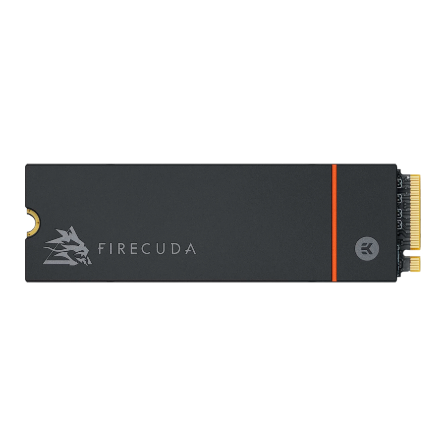
Figure 1 FireCuda 530 SSD M2 2280-D2-M Top View

Figure 2 FireCuda 530 SSD M2 2280-D2-M Side View

Figure 3 FireCuda 530 SSD M2 2280-D2-M Bottom View

Figure 4 FireCuda 530 SSD M2 2280-S2-M Top View

Figure 5 FireCuda 530 SSD M2 2280-S2-M Side View

Figure 6 FireCuda 530 SSD M2 2280-S2-M Bottom View

Figure 7 FireCuda 530 SSDs with Heatsink (500 GB and 1000 GB)

Figure 8 FireCuda 530 SSDs with Heatsink (2000 GB)

Figure 9 FireCuda 530 SSDs with Heatsink (4000 GB)
Pin and Signal Descriptions
Table 9 Pin Descriptions
| Pin No. | PCIe Pin | Description |
| 1 | GND | CONFIG_3 = GND |
| 2 | 3.3V | 3.3V source |
| 3 | GND | Ground |
| 4 | 3.3V | 3.3V source |
| 5 | PETn3 | PCIe TX Differential signal defined by the PCI Express M.2 spec |
| 6 | N/C | No connect |
| 7 | PETp3 | PCIe TX Differential signal defined by the PCI Express M.2 spec |
| 8 | N/C | No connect |
| 9 | GND | Ground |
| 10 | LED1# | Open drain, active low signal. These signals are used to allow the add- in card to provide status indicators via LED devices that will be provided by the system. |
| 11 | PERn3 | PCIe RX Differential signal defined by the PCI Express M.2 spec |
| 12 | 3.3V | 3.3V source |
| 13 | PERp3 | PCIe RX Differential signal defined by the PCI Express M.2 spec |
| 14 | 3.3V | 3.3V source |
| 15 | GND | Ground |
| 16 | 3.3V | 3.3V source |
| 17 | PETn2 | PCIe TX Differential signal defined by the PCI Express M.2 spec |
| 18 | 3.3V | 3.3V source |
| 19 | PETp2 | PCIe TX Differential signal defined by the PCI Express M.2 spec |
| 20 | N/C | No connect |
| 21 | GND | Ground |
| 22 | N/C | No connect |
| 23 | PERn2 | PCIe RX Differential signal defined by the PCI Express M.2 spec |
| 24 | N/C | No connect |
| 25 | PERp2 | PCIe RX Differential signal defined by the PCI Express M.2 spec |
| 26 | N/C | No connect |
| 27 | GND | Ground |
| 28 | N/C | No connect |
| 29 | PETn1 | PCIe TX Differential signal defined by the PCI Express M.2 spec |
| 30 | N/C | No connect |
| 31 | PETp1 | PCIe TX Differential signal defined by the PCI Express M.2 spec |
| 32 | N/C | No connect |
| 33 | GND | Ground |
| 34 | N/C | No connect |
| 35 | PERn1 | PCIe RX Differential signal defined by the PCI Express M.2 spec |
| 36 | N/C | No connect |
| 37 | PERp1 | PCIe RX Differential signal defined by the PCI Express M.2 spec |
| 38 | N/C | No connect |
| 39 | GND | Ground |
| 40 | SMB_CLK (I/O)(0/1.8V) | SMBus Clock; Open Drain with pull-up on platform |
| 41 | PETn0 | PCIe TX Differential signal defined by the PCI Express M.2 spec |
| 42 | SMB_DATA (I/O)(0/1.8V) | SMBus Data; Open Drain with pull-up on platform. |
| 43 | PETp0 | PCIe TX Differential signal defined by the PCI Express M.2 spec |
| 44 | ALERT#(O) (0/1.8V) | Alert notification to master; Open Drain with pull-up on platform; Active low. |
| 45 | GND | Ground |
| 46 | N/C | No connect |
| 47 | PERn0 | PCIe RX Differential signal defined by the PCI Express M.2 spec |
| 48 | N/C | No connect |
| 49 | PERp0 | PCIe RX Differential signal defined by the PCI Express M.2 spec |
| 50 | PERST#(I)(0/3.3V) | PE-Reset is a functional reset to the card as defined by the PCIe Mini CEM specification. |
| 51 | GND | Ground |
| 52 | CLKREQ#(I/O)(0/3.3V) | Clock Request is a reference clock request signal as defined by the PCIe Mini CEM specification; Also used by L1 PM Sub-states. |
| 53 | REFCLKn | PCIe Reference Clock signals (100 MHz) defined by the PCI Express M.2 spec. |
| 54 | PEWAKE#(I/O)(0/3.3V) | PCIe PME Wake. Open Drain with pull up on platform; Active Low. |
| 55 | REFCLKp | PCIe Reference Clock signals (100 MHz) defined by the PCI Express M.2 spec. |
| 56 | Reserved for MFG DATA | Manufacturing Data line. Used for SSD manufacturing only. Not used in normal operation. Pins should be left N/C in platform Socket. |
| 57 | GND | Ground |
| 58 | Reserved for MFG CLOCK | Manufacturing Clock line. Used for SSD manufacturing only. Not used in normal operation. Pins should be left N/C in platform Socket. |
| 59 | Module Key M | Module Key |
| 60 | Module Key M | |
| 61 | Module Key M | |
| 62 | Module Key M | |
| 63 | Module Key M | |
| 64 | Module Key M | |
| 65 | Module Key M | |
| 66 | Module Key M | |
| 67 | N/C | No connect |
| 68 | SUSCLK(32KHz) (I)(0/3.3V) | 32.768 kHz clock supply input that is provided by the platform chipset to reduce power and cost for the module. |
| 69 | N/C | PEDET (NC-PCIe) |
| 70 | 3.3V | 3.3V source |
| 71 | GND | Ground |
| 72 | 3.3V | 3.3V source |
| 73 | GND | Ground |
| 74 | 3.3V | 3.3V source |
| 75 | GND | Ground |
NVMe Commands
Table 10 Admin Commands
| Identifier | O/M | Command Description | Supported |
| 00h | M | Delete I/O Submission Queue | Supported |
| 01h | M | Create I/O Submission Queue | Supported |
| 02h | M | Get Log Page | Supported |
| 04h | M | Delete I/O Completion Queue | Supported |
| 05h | M | Create I/O Completion Queue | Supported |
| 06h | M | Identify | Supported |
| 08h | M | Abort | Supported |
| 09h | M | Set Feature | Supported |
| 0Ah | M | Get Feature | Supported |
| 0Ch | M | Asynchronous Event Request | Supported |
| 10h | O | Firmware Commit | Supported |
| 11h | O | Firmware Image Download | Supported |
| 14h | O | Device Self-test | Supported |
| 80h | O | Format NVM | Supported |
| 81h | O | Security Send | Supported |
| 82h | O | Security Receive | Supported |
| 84h | O | Sanitize | Supported |
Table 11 I/O Commands
| Identifier | O/M | Command Description | Supported |
| 00h | O | Flush | Supported |
| 01h | O | Write | Supported |
| 02h | O | Read | Supported |
| 04h | O | Write Uncorrectable | Not Supported |
| 05h | O | Compare | Supported |
| 08h | O | Write Zeroes | Supported |
| 09h | O | Dataset Management | Supported |
Table 12 Set Feature Commands
| Identifier | O/M | Command Description | Supported |
| 00h | Reserved | ||
| 01h | M | Arbitration | Supported |
| 02h | M | Power Management | Supported |
| 03h | O | LBA Range Type | Not Supported |
| 04h | M | Temperature Threshold | Supported |
| 05h | M | Error Recovery | Supported |
| 06h | O | Volatile Write Cache | Supported |
| 07h | M | Number Of Queues | Supported |
| 08h | M | Interrupt Coalescing | Supported |
| 09h | M | Interrupt Vector Configuration | Supported |
| 0Ah | M | Write Atomicity Normal | Supported |
| 0Bh | M | Asynchronous Event Configuration | Supported |
| 0Ch | O | Autonomous Power State Transition | Supported |
| 0Dh | O | Host Memory Buffer | Not Supported |
| 0Eh | O | Timestamp | Supported |
| 10h | O | Host Controlled Thermal Management | Supported |
| 11h | O | Non-Operational Power State Config | Supported |
| 0Eh - 7Dh | Reserved | ||
| 80h | O | Software Progress Marker | Supported |
Table 13 Get Log Page Commands
| Identifier | O/M | Command Description | Supported |
| 00h | Reserved | ||
| 01h | M | Error Information | Supported |
| 02h | M | SMART / Health Information | Supported |
| 03h | M | Firmware Slot Information | Supported |
| 04h | O | Changed Namespace List | Supported |
| 06h | O | Device Self-test | Supported |
| 09h - 7Fh | Reserved | ||
| 81h | O | Sanitize Status | Supported |
| 82h - FFh | Reserved |
SMART Support
The FireCuda 530 SSD supports the SMART command set.
SMART Attributes
The following table lists SMART Attributes and Descriptions.
Table 14 SMART Attributes (Log Identifier 02h)
| Bytes Index | Bytes | Description |
| [0] | 1 | Critical Warning |
| [2:1] | 2 | Composite Temperature |
| [3] | 1 | Available Spare |
| [4] | 1 | Available Spare Threshold |
| [5] | 1 | Percentage Used |
| [31:6] | 26 | Reserved |
| [47:32] | 16 | Data Units Read |
| [63:48] | 16 | Data Units Written |
| [79:64] | 16 | Host Read Commands |
| [95:80] | 16 | Host Write Commands |
| [111:96] | 16 | Controller Busy Time |
| [127:112] | 16 | Power Cycles |
| [143:128] | 16 | Power On Hours |
| [159:144] | 16 | Unsafe Shutdowns |
| [175:160] | 16 | Media and Data Integrity Errors |
| [191:176] | 16 | Number of Error Information Log Entries |
| [195:192] | 4 | Warning Composite Temperature Time |
| [199:196] | 4 | Critical Composite Temperature Time |
| [201:200] | 2 | Temperature Sensor 1 (Current Temperature) |
| [203:202] | 2 | Temperature Sensor 2 (N/A) |
| [205:204] | 2 | Temperature Sensor 3 (N/A) |
| [207:206] | 2 | Temperature Sensor 4 (N/A) |
| [209:208] | 2 | Temperature Sensor 5 (N/A) |
| [211:210] | 2 | Temperature Sensor 6 (N/A) |
| [213:212] | 2 | Temperature Sensor 7 (N/A) |
| [215:214] | 2 | Temperature Sensor 8 (N/A) |
| [511:216] | 296 | Reserved |
NOTES
For (Log Identifier 02h:
- "Critical Warning [Byte 0]"
- This field indicates critical warnings for the state of the controller.
- Bit#0: Available spare is below threshold
- Bit#1: Temperature exceeded threshold or below an under temperature threshold
- Bit#2: Reliability is degraded due to excessive media or internal errors
- Bit#3: Media is placed in read only mode
- BIt#4: Volatile memory backup device has failed.
- Bit#5 - Bit#7: Reserved
- "Available Spare [Byte 3]" Value (percentage) = 100* [(total reserved VB - consumed VB caused by early, later bad)/ total reserved VB]
- "Percentage Used [Byte 5]"
- Value (percentage) = 100* (total VB erase count/ PE cycle for total VB)
Table 15 SMART Attributes (Log Identifier C0h)
| Bytes Index | Bytes | Description |
| [7:0] | 8 | Device Capacity |
| [15:8] | 8 | User Capacity |
| [23:16] | 8 | NAND Read |
| [31:24] | 8 | NAND Write |
| [39:32] | 8 | NAND Erase Sector |
| [47:40] | 8 | SSD Life Remaining Percent D3 |
| [55:48] | 8 | SSD Life Used Percent D3 |
| [56] | 1 | WP Water Mark |
| [58:57] | 2 | Highest temperature |
| [62:59] | 4 | Flash UNC Error Count |
| [67:63] | 5 | Data E3D Error |
| [70:67] | 4 | PHY Error Count |
| [74:71] | 4 | Total Bad Block Count |
| [78:75] | 4 | Total Early Bad Block Count |
| [82:79] | 4 | Total Later Bad Block Count |
| [86:83] | 4 | Read Fail Count |
| [90:87] | 4 | Program Fail Count |
| [94:91] | 4 | Erase Failure Count |
| [102:95] | 8 | System Table Copy Count |
| [110:103] | 8 | Read Move Table Count |
| [114:111] | 4 | Data read retry count |
| [118:115] | 4 | RAID ECC retry count |
| [122:119] | 4 | RAID ECC failed count |
| [130:123] | 8 | Total Erase Count |
| [134:131] | 4 | Max Erase Count |
| [138:135] | 4 | Average Erase Count |
| [142:139] | 4 | Min Erase Count |
| [150:143] | 8 | Background read count |
| [154:151] | 4 | Host Write Uncorrectable Sector Count |
| [158:155] | 4 | PS3 Enter Success |
| [162:159] | 4 | PS4 Enter Success |
| [166:163] | 4 | Wear Leveling Count |
| [167] | 1 | Chip internal temperature |
| [169:168] | 2 | Thermal throttling |
| [171:170] | 2 | Thermal throttling time |
| [179:172] | 8 | FW Code Update Count |
| [511:181] | 331 | RSV |
NOTES
For Log Identifier C0h:
- "SSD Life Remaining Percent D3 [Byte 47:40]"
- Value (percentage) = 100 *[1 - (Average of the Flash's block erase count / NAND EOL erase count)]
- "SSD Life Used Percent [Byte 55:48]"
- Value (percentage) = 100 *(Average of the Flash's block erase count / NAND EOL erase count)
Feature Details
Flash Management
Error Correction Code
Flash memory cells will deteriorate with use, which might generate random bit errors in the stored data. Thus, FireCuda 530 SSD applies the fourth generation LDPC(Low Density Parity Check) of ECC algorithm, which can detect and correct errors that occur during read process, ensure data has been read correctly, as well as protect data from corruption.
Wear Leveling
NAND flash devices can only undergo a limited number of program/erase cycles, and in most cases, the flash media are not used evenly. If some areas get updated more frequently than others, the lifetime of the device would be reduced significantly. Thus, Wear Leveling is applied to extend the lifespan of NAND Flash by evenly distributing write and erase cycles across the media.
Seagate provides advanced Wear Leveling algorithm, which can efficiently spread out the flash usage through the whole flash media area. Moreover, by implementing both dynamic and static Wear Leveling algorithms, the life expectancy of the NAND flash is greatly improved.
Bad Block Management
Bad blocks are blocks that do not function properly or contain more invalid bits causing stored data to become unstable, and their reliability is not guaranteed. Blocks that are identified and marked as bad by the manufacturer are referred to as "Early Bad Blocks". Bad blocks that are developed during the lifespan of the flash are named "Later Bad Blocks". Seagate implements an efficient bad block management algorithm to detect the factory- produced bad blocks and manages bad blocks that appear with use. This practice prevents data being stored into bad blocks and further improves the data reliability.
TRIM
TRIM is a feature which helps improve the read/write performance and speed of solid-state drives (SSD). Unlike hard disk drives (HDD), SSDs are not able to overwrite existing data, so the available space gradually becomes smaller with each use. With the TRIM command, the operating system can inform the SSD which blocks of data are no longer in use and can be removed permanently. Thus, the SSD will perform the erase action, which prevents unused data from occupying blocks all the time.
SMART
SMART, an acronym for Self-Monitoring, Analysis and Reporting Technology, is an open standard that allows a hard disk drive to automatically detect its health and report potential failures. When a failure is recorded by SMART, users can choose to replace the drive to prevent unexpected outage or data loss. Moreover, SMART can inform users of impending failures while there is still time to perform proactive actions, such as copy data to another device.
Over Provisioning
Over Provisioning refers to the inclusion of extra NAND capacity in a SSD, which is not visible and cannot be used by users. With Over Provisioning, the performance and IOPS (Input/output Operations per Second) are improved by providing the controller additional space to manage P/E cycles, which enhances the reliability and endurance as well. Moreover, the write amplification of the SSD becomes lower when the controller writes data to the flash.
Firmware Upgrade
Firmware can be considered as a set of instructions on how the device communicates with the host. Firmware will be upgraded when new features are added, compatibility issues are fixed, or read/write performance gets improved.
Thermal Throttling
The purpose of thermal throttling is to prevent any components in a SSD from over-heating during read and write operations. The device is designed with an on-die and an on-board thermal sensor, and with its accuracy, firmware can apply different levels of throttling to achieve the purpose of protection efficiently and proactively via SMART reading.
Table 16 Current version: Thermal Throttling 2.0
| Item | Content |
| Reference of temp. reading | On-board thermal sensor, Controller on-die thermal sensor |
| tmt1 threshold (PE < 500) | 82°C per Smart reported |
| tmt2 threshold (PE < 500) | 85°C per Smart reported |
| tmt1 threshold (PE > 500) | 68°C per Smart reported |
| tmt2 threshold (PE > 500) | 70°C per Smart reported |
| Protect controller threshold | 115°C from on-die thermal sensor |
| Fatal threshold | 120°C from on-die thermal sensor |
| Resume performance threshold (PE < 500) | 78°C per Smart reported |
| Resume performance threshold (PE > 500) | 64°C per Smart reported |
| Temperature polling frequency | Every 1 sec |
| TMT1_state impact | ±10% CE |
| TMT2_state impact | -20% CE |
NOTE
For optimal performance:
- Provide sufficient airflow and cooling.
Advanced Device Security Features
NVMe format
Secure Erase is a standard NVMe format command and it writes all "0xFF" to fully wipe all the data on the SSDs. When this command is issued, the SSD controller erases its storage blocks and returns the drive to its factory default settings.
Sanitize Operation
The Sanitize feature is an alternative to the existing secure erase capabilities through the Format NVM command and makes a robust data security by ensuring the user data from the drive's media, caches and the Controller Memory Buffer are all wiped by the block erase operations, overwriting or destroying the encryption key. The following table illustrates the types of Sanitize Operations supported.
Table 17 Supported Sanitize Operations
| Drive Security Type | Sanitize Operation | ||
| Overwrite | Block Erase | Crypto Erase | |
| Non-SED | Yes | Yes | No |
NOTE
Sanitize Overwrite command completion takes at least one hour per terabyte per pass. The number of passes is drive-selectable. The NVMe spec default is 16 passes. Contact Seagate Support for more detailed information.
Product Lifetime Management
Total Bytes Written
TBW (total bytes written) is a measurement of the SSDs' expected lifespan, which represents the amount of data written to the device. To calculate the TBW of a SSD, the following equation is applied:
TBW = [(NAND Endurance) x (SSD Capacity)] / WAF
NAND Endurance: NAND endurance refers to the P/E (Program/Erase) cycle of a NAND flash. SSD Capacity: The SSD capacity is the specific capacity in total of a SSD.
WAF: Write Amplification Factor (WAF) is a numerical value representing the ratio between the amount of data that a SSD controller needs to write and the amount of data that the host's flash controller writes. A better WAF, which is near 1, guarantees better endurance and lower frequency of data written to flash memory.
Media Wear Indicator
Actual life indicator reported by SMART Attribute byte index [5], Percentage Used, recommends User to replace drive when reaching to 100%.
Read Only Mode
End of Life
When drive is aged by cumulated program/erase cycles, media worn- out may cause increasing numbers of later bad block. When the number of available spare is less the threshold(5%, SMART attribute log ID 02h Byte4), the drive will notify Host through AER event and Critical Warning to enter Read Only Mode to prevent further data corruption. User should start to replace the drive with another one immediately.
An Adaptive Approach to Performance Tuning
Throughput
Based on the available space of the disk, the drive will regulate the read/write speed and manage the performance of throughput. When there still remains a lot of space, the firmware will continuously perform read/write action. There is still no need to implement garbage collection to allocate and release memory, which will accelerate the read/write processing to improve the performance. Contrarily, when the space is being used up, the drive will slow down the read/write processing, and implement garbage collection to release memory. Hence, read/write performance will become slower.
Predict & Fetch
Normally, when the Host tries to read data from the PCIe SSD, the PCIe SSD will only perform one read action after receiving one command. However, the drive applies Predict & Fetch to improve the read speed. When the host issues sequential read commands to the PCIe SSD, the PCIe SSD will automatically expect that the following will also be read commands. Thus, before receiving the next command, flash has already prepared the data. Accordingly, this accelerates the data processing time, and the host does not need to wait so long to receive data.
SLC Caching
The firmware design of the device currently adopts dynamic caching to deliver better performance for better endurance and consumer user experience. The SLC caching size is up to 1/3 of free capacity of the SSD.
Product Installation Precautions
Device Handling Instructions
There are a lot of components assembled on a single SSD device. Handle the drive with care especially when it has any WLCSP (Wafer Level Chip Scale Packaging) components such as PMIC, thermal sensor or load switch. WLCSP is a packaging technology widely used for making smaller footprints. However, any bumps or scratches may damage those ultrasmall parts so you must handle with gentle care. See Figure 9.2, FireCuda 530 SSD Installation Instructions

DO NOT DROP SSD
INSTALL SSD WITH CARE
STORE SSD IN A PROPER PACKAGE
Device Installation Instructions
FireCuda 530 features the PCIe connector with M-key, which is compatible only with the M-key socket. See Use Case 1 in Figure 10, M-Key M.2 Assembly Precautions. As shown in Use Case 2, misuse may cause severe damage to an SSD including burn-out.

Heatsink Disclosures
NOTE
About Heatsink SSDs.
- Heatsinks are pre-installed. Do not remove the heatsink; you can damage the SSD.
- Dimensions exceed standard size specifications for the M.2 without a heatsink. Please verify that your system has enough space for installation.
- SSDs with heatsinks are recommended for M.2 with connectors H3.2 and above.
Seagate Technology LLC
AMERICAS Seagate Technology LLC 47488 Kato Road, Fremont, California 94538, United States, 510-661-1000
ASIA/PACIFIC Seagate Singapore International Headquarters Pte. Ltd. 90 Woodlands Avenue 7, Singapore 737911, 65-6412-3666
EUROPE, MIDDLE EAST AND AFRICA Seagate Technology (Netherlands) B.V. Koolhovenlaan 1, 1119 NB Schiphol-Rijk, Netherlands, 31-20-316-7300
Documents / Resources
References
Productondersteuning | Seagate Nederland
Software- en firmwaredownloads | Seagate Nederland
Contact | Seagate Nederland
Garantie en vervangingen | Seagate Nederland
Contact | Seagate Nederland
Seagate-partners | Seagate Nederland
Seagate Support | Seagate Nederland
Download manual
Here you can download full pdf version of manual, it may contain additional safety instructions, warranty information, FCC rules, etc.
Advertisement


Need help?
Do you have a question about the FireCuda 530 SSD and is the answer not in the manual?
Questions and answers