Table of Contents
Advertisement
Quick Links
Advertisement
Table of Contents

Related Manuals for Hytera AP589EG


Summary of Contents for Hytera AP589EG
- Page 1 AP589EG...
- Page 2 Preface This manual describes the information related to the product repair. It is intended for use by qualified technicians only. Before repairing the product properly, please read this manual carefully. This manual is applicable to the following product: AP58X Two-way Radio (X may represent 2, 5, 6, 8,9 or 9EG)
-
Page 3: Copyright Information
Copyright Information Hytera is the trademark or registered trademark of Hytera Communications Corporation Limited (the Company) in the People's Republic of China (PRC) and/or other countries or areas. The Company retains the ownership of its trademarks and product names. All other trademarks and/or product names that may be used in this manual are properties of their respective owners. -
Page 4: Documentation Information
Documentation Information This section describes the conventions and revision history of this document. Conventions Instruction Conventions Icon Description Indicates information that can help you make better use of your product. Indicates references that can further describe the related topics. Indicates situations that could cause data loss or equipment damage. Indicates situations that could cause minor personal injury. -
Page 5: Revision History
Revision History Version Release Date Description March 2022 Initial release. - Page 6 VHF (136–174 MHz)
-
Page 7: Table Of Contents
VHF (136–174 MHz) Contents Contents 1. Product Layout ............................1 2. Disassembly and Reassembly ......................2 2.1 Tools ..............................2 2.2 Procedure ............................2 3. Exploded View and Packaging Guide....................5 3.1 Exploded View ........................... 5 3.2 Packaging Guide ..........................7 4. -
Page 8: Product Layout
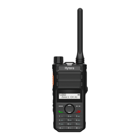
VHF (136–174 MHz) Product Layout 1. Product Layout Part Name Part Name Part Name Channel Selector Knob Speaker Contact Key Push-to-Talk (PTT) Key Microphone Keypad Volume Up Key LCD Display Accessory Connector Volume Down Key OK/Menu Key USB Type-C Port Side Key 3 (SK3) Up Key Strap Hole... -
Page 9: Disassembly And Reassembly
Disassembly and Reassembly VHF (136–174 MHz) 2. Disassembly and Reassembly This section introduces how to disassemble the radio. To reassemble the radio, do vice versa. 2.1 Tools Socket wrench Torx screwdriver Tweezers Soldering iron 2.2 Procedure Make sure the waterproof ring is attached in place during reassembly. - Page 10 VHF (136–174 MHz) Disassembly and Reassembly Solder Joint of Speaker Solder Joint of Microphone Use tweezers to remove the male FPC connectors and LCD connector, and then remove the main board. Male FPC Connector LCD Connector Rotate the antenna counter-clockwise to remove it, pull out the Channel Selector knob, and then use a socket wrench to remove the nuts from the Channel Selector knob.
- Page 11 Disassembly and Reassembly VHF (136–174 MHz) Use a Torx screwdriver to pry off the LCD bracket, and then remove the LCD bracket and LCD display. Use a Torx screwdriver to remove the four screws on the keypad, and then remove the keypad.
-
Page 12: Exploded View And Packaging Guide
VHF (136–174 MHz) Exploded View and Packaging Guide 3. Exploded View and Packaging Guide 3.1 Exploded View Parts list: Part No. Description Qty. Part No. Description Qty. 5107000000477B Metric screw 11500000059471 Audio accessory board Waterproof ring for 5110000000402A 5113010081525A Earpiece PC sheet machine screw Adhesive tape for LCD 5117000081542A... - Page 13 Exploded View and Packaging Guide VHF (136–174 MHz) Part No. Description Qty. Part No. Description Qty. Silicone rubber Silicone rubber PTT 5110000000265A 5110020081520A emergency key Emergency key 5116000081584A 5116000081705A Side key bracket bracket 5107020060322A Anti-loose nut 5116000000229A PTT key cover Waterproof ring for 5110000000558A 5107000000026A...
-
Page 14: Packaging Guide
VHF (136–174 MHz) Exploded View and Packaging Guide 3.2 Packaging Guide... -
Page 15: Specifications
Specifications VHF (136–174 MHz) 4. Specifications General Frequency Range 136–174 MHz Dimensions (H x W x D) (with battery and without 115 mm x 55 mm x 29.5 mm antenna) Weight (with battery and antenna) 230 g (±5%) Zone Capacity Channel Capacity Channel Spacing 12.5 KHz/20 KHz/25 KHz... - Page 16 VHF (136–174 MHz) Specifications TX Section Frequency Stability ±0.5 ppm Power Output High 11K0F3E@12.5 kHz FM Modulation 14K0F3E@20 kHz 16K0F3E@25 kHz 12.5 kHz (data only): 7K60FXD 4FSK Modulation 12.5 kHz (data and voice): 7K60FXW –36 dBm < 1 GHz Spurious Emission –30 dBm >...
- Page 17 Specifications VHF (136–174 MHz) All specifications are tested according to applicable standards, and subject to change without notice due to continuous technological development.
-
Page 18: Circuit Description
VHF (136–174 MHz) Circuit Description 5. Circuit Description 5.1 Baseband Section 5.1.1 Power Supply Module RF PA TX_EN 3V3A_TX U2011 TYPE_C Audio PA U3010 3V3A_RX U2008 2000mA VSYS 3V6D FGU_EN ( 1800mA ) (1200mA) DCDC Charge 3V3A_FGU U2002 U2009 U2506 POWER_ON POWER_ON 3V3A_MIC... -
Page 19: Control Module
Circuit Description VHF (136–174 MHz) The test points and voltage range of each power supply are shown in the table below. Network Test Point Voltage Range (V) 3V3D_BT TP9505 3.3±10% V 3V6D L2008 3.6±10% V 5VA_FGU FB2015 5±10% V 3V3A_TX FB2088 3.3±10% V 3V3A_MIC... -
Page 20: Audio Module
VHF (136–174 MHz) Circuit Description 5.1.3 Audio Module Green : Transmit Path Blue : Receive Path RF UNIT BT_SPKP AU_AUXMIC_P BT_MICP BT_SPKN AU_AUXMIC_N MICLP Codec BT_SPKP SPKRP BT_MICN BT_SPKN MICLN (Built-in A7) SPKRN INT_MICP AU_MIC_P INT_MICN EXT_MICP AU_MIC_N EXT_MICN AU_RCVP AU_RCVN Speaker TPA3131... -
Page 21: Audio Power Amplifier
Circuit Description VHF (136–174 MHz) Audio Power Amplifier The table below lists the main parameters of the audio amplifier. Parameter Value Rated power (P Maximum power (P 3.5 W max) 8 Ω Speaker Impedance (R 5.2 RF Section 5.2.1 TX Circuit Drive-stage Final-stage Pre-Driver PA Match... -
Page 22: Apc Circuit
VHF (136–174 MHz) Circuit Description harmonics and spurious signals. Finally, it goes to the antenna for transmission. APC Circuit The APC circuit converts the drain current from the driver-stage PA and final-stage PA into a voltage, and then compares the voltage with the APC control voltage output by the MCU. The error voltage generated from the comparison adjusts the TX power by controlling the gate bias voltage of the driver-stage PA and final-stage PA. -
Page 23: Fgu Circuit
Circuit Description VHF (136–174 MHz) RX Back-End The amplified RF signal goes to the A7, in which it is further amplified by the LNA and mixes with the VCO signal to generate a zero IF signal. The zero IF signal goes to the PGA and filter, and is converted into a digital signal by the ADC. -
Page 24: Troubleshooting Flowchart
VHF (136–174 MHz) Troubleshooting Flowchart 6. Troubleshooting Flowchart 6.1 Control Circuit Start Is power-on Is th e RF circuit The control circu it is indication nor mal? [1] driven nor mal ly? [2] normal. Check RF power supply circuits U2008, U2009, U201 1, and U201 3, and control ci rcui t Is 3V6D n ormal? [3] Check U2002... -
Page 25: Rx Circuit
Troubleshooting Flowchart VHF (136–174 MHz) 6.2 RX Circuit Start Is output of 3V3A_RX Is output of R3V3 normal? [2] Check U2008 normal? [1] Check U6003 Is t he quiescent operating point of Check Q6000 Q6000 normal? [3] Check whether the RF Is RF signal sensitivity in t he test connector of CARKI T is at RF connector of CARKI T... -
Page 26: Tx Circuit
VHF (136–174 MHz) Troubleshooting Flowchart [5] Confirm the RF signal output at Q6000. For example, input a –123 dBm RF signal at the RF connector of CARKIT, the output amplitude of LNA_OUT2 at Q6000 is about –115 dBm. [6] U6001 and U6002 are toggle switches. When the radio is receiving signals normally, LNA_H_En will output a control voltage of 3.3 V, and Pin 4 of U6001 and Pin 6 of U6002 are at high level. - Page 27 Troubleshooting Flowchart VHF (136–174 MHz) Start Check the power sup ply Is th e p ower supp ly normal? circuit Is th e curre nt or VGG Check the voltage of chip Is TX_En normal? [3] normal? [2] output pin Check the voltage of chip Is APC normal? [8] output pin...
- Page 28 VHF (136–174 MHz) Troubleshooting Flowchart [2] When the radio operates in low power mode, the current ranges from 0.6 A to 0.9 A. When the radio operates in high power mode, the current ranges from 1.4 A to 1.9 A. [3] The voltage at TX_En is about 3.3±10% V.
-
Page 29: Interface Definition
Interface Definition VHF (136–174 MHz) 7. Interface Definition The table below lists information about the 9-pin accessory connector. Pin No. Signal Description Illustration SPK+ External speaker + SPK– External speaker - UART pin UART pin 1.SPK+ General ground 2.SPK- 3.TXD Accessory identifier 1_wire 4.RXD 1_WIRE/GPIO... -
Page 30: Tuning Description
VHF (136–174 MHz) Tuning Description 8. Tuning Description 8.1 Tools Radio communication test set: Aeroflex 3920 and HP8921 Power supply: 3 A/10 V Multimeter A6 Tuner software 8.2 Tuning Procedure 8.2.1 Tuning the Radio After reassembling the radio, tune it using the A6 Tuner software. The table below describes the items to be tuned and the corresponding tuning methods. -
Page 31: Pcb View
9. PCB View Main Board_Top Layer... - Page 32 Main Board_Bottom Layer...
-
Page 33: Block Diagram
Block Diagram VHF (136–174 MHz) 10. Block Diagram Reserved DACH SPI1 UART1 Flow Control 52MHz XTAL UART_HOST External PTT GPIO4 KEYIN0-4 KEYOUT0-4 Earpiece Detection GPIO7 KEYPAD BT_MIC AUDIO EMC SK1 SK2 KEYIN1 AU_HPR KEYOUT0-2 BUTTON GPIO1 Interrupt AUX_MIC INT_MIC Knob Switch GPIO3,6,9,10 Interrupt SWITCH... -
Page 34: Schematic Diagram
POWER_charge 11. Schematic Diagram USB_DP TP2112 J2101 FB2214 120R/100MHZ/1300mA GND1 VBUS1 VBUS FB2206 120R/100MHZ/1300mA GND2 VBUS2 R2588 10R/F HOST_TXD1 (11) C2102 R2101 10R/F USB_DP (7) C2656 0.1uF/16V R2589 10R/F 270pF/25V HOST_RXD1 (11) R2102 10R/F USB_DM (7) SBU1 SBU2 MUP-U22401-2 TP2111 USB_DM VSYS C2008... - Page 35 POWER_CTRL TP2100 BAT+ TP2101 BAT_THERM TP2114 BAT+ J2100 BAT_THERM (3,6) C2116 470pF/25V D2112 C17200 ESD9N5BM VSYS 3V3D R2116 R2115 R2123 100K/J 560K/J 10K/J Q2115 PWR_KEY_DET PWR_ON PMZ350UPE TP2102 D2100 R2120 BAS16XV2T1G 100K/J D2217 R2282 BAS16XV2T1G (11) PWR_KEY 100K/J R2777 100K/J D2317 D2107 (5,7)
- Page 36 POWER_LDO 3V6D 3V3A_RX VSYS U2002 L2559 U2008 FB2008 4.7uH/2.85A 3V6D VOUT BOOT C2015 C2016 C2017 C2018 L2003 L2008 C2058 120R/100Mhz/450mA C2077 C2889 0.1uF/16V 3.3uH/1A C2062 VSS2 4.7uF/25V 0.1uF/16V 22uF/25V 16V/2.2 uF C2125 22uF/25V 22uF/25V PWR_ON (4,6) 4.7uH/2.85A 16V/2.2 uF 0.1uF/16V C2019 C2023 R2321...
- Page 37 A7-POWER R1105 220K/F R1106 220K/F R1121 0R/F BAT+ R1112 10K/J VBUS PWR_ON (4,5) D1102 L1100 V_CORE V_FPGA V_MIC V_RTC BBPLL_TEST 4.7uH/300mA C1103 C1101 C1102 LO_TEST SW_BUCK1 SW_BUCK2 22uF/10V 0.1uF/16V 2700pF/50V ANA_TEST_EN V_CORE1 V_CORE2 CHARGER TST_H V_CORE3 L1101 VBUCK2_2V4 EFUSE R1103 10K/J PROG_EFUSE1 SW_BUCK2_1...
- Page 38 A7_CTRL 3V3D 3V3D 3V3D R1294 R1295 100K/J R1296 100K/J 1_Wire_EXT (11) Q1203 U1201 R1293 LCD_ID2/1_W IRE_CTRL (7,11) Vcca Vccb UART2_TXD_EXT (11) UART2_RXD_EXT (11) UART2_TXD UART2_RXD 1_Wire 10R/J 2SK3019 2SK3019 Q1201 R1298 0R/F Q1202 2SK3019 TXS0102DCU/NC D1201 NC R1297 0R/F R1291 R1229 100R/J TD_ON (11)
- Page 39 CODEC TP3001 RCV_SPKP R3001 0R/F C3055 C3056 10K/J 10K/J R3002 0R/F U3009 R3086 0.47uF/6.3V AMP_INPR SPKP U3001 COM1 R3087 0.47uF/6.3V RCV_SPKP AMP_INNR R3003 1.5K/F SPKP RCV_SPKP SPKP (8) SPKN COM1 COM2 RCV_SPKN SPKN R3004 1.5K/F RCV_SPKN SPKN (8) R3152 0R/F COM2 (7,9) AUD_SW...
- Page 40 U3004 AU_MICN AF_BT_EARP (10) COM1 AUD_SW=0:EXT_MIC ENABLE AU_MICP AF_BT_EARN (10) COM2 AUD_SW=1:INT_MIC ENABLE R3054 BT_AUDIO_SW U3002 33R/J INT_MICN R3055 0R/F INT_MIC 3V3A SSCAP COM1 INT_MICP COM2 C3091 R3053 R3015 1K/J 0.1uF/16V (7,8) AUD_SW SGM2268 33R/J R3000 0R/F 3V3A EXT_MICN (11) SSCAP EXT_MIC EXT_MICP (11)
- Page 41 3V3D_BT BT_SWS BT_USB_DP BT_USB_DM R9579 R9580 DC5V 10K/J 10K/J J9504 C9531 R9527 BT_RF BT_UART_TXD R9543 33R/J UART1_RXD_BT BT_UART_TXD 33pF/50V 0R/F BT_UART_RXD R9544 33R/J UART1_TXD_BT BT_UART_RXD BT_EARP BT_EARP BT_EARN BT_EARN 818002935 J9505 BT_MIC+ U9504 I2S_DIN/SPI_MOSI BT_MICP BT_MIC- I2S_DOUT/SPI_MISO BT_MICN TLSR9513C I2S_SCK/SPI_CLK I2S_DWS/SPI_CS BT_MICP0 BT_MICN0_AGND...
- Page 42 INTERFACE 120R/100MHZ/1300mA BL_LED_OUT C5145 J5101 C5110 R5130 L5101 C5111 LED-LCD-BL BL_LED_OUT 0.1uF/16V 0.1uF/16V R5131 16V/2.2 uF L5102 120R/100Mhz/450mA OK_14F016_04 C5144 C5133 0.1uF/16V R5142 10K/J LCD_ID1 R5112 1K/J R5102 1K/J 16V/2.2 uF R5144 (7,11) KROW1 LCD_ID2/1_WIRE_CTRL KCOL1 (7) R5113 1K/J R5108 1K/J R5139 100R/J...
- Page 43 RX-FRONT-END C6000 C6001 C6002 C6003 C6004 C6005 [13] LNA_IN_1 1000PF/50V 56PF/50V 22pF/50V 20pF/50V 39pF/50V 1000pF/25V C6006 C6007 C6008 C6009 C6010 C6011 68pF/50V 47pF/50V U6000 50V/220PF 1000PF/50V RB706F-40(T106) 1000pF/25V 1000pF/25V L6000 L6001 L6002 72nH/400mA 56nH/600mA 68nH/0.34A L6003 [12] LNA_IN_2 LNA_H_En 120R/100Mhz/450mA C6012 1000pF/25V C6013...
- Page 44 TX PATH FB7001 3V3A_TX 180R/100MHz/1500mA 7V4_PA R7000 R7001 100R/J 100R/J FB9509 180R/100MHz/1500mA C7004 C7005 1000pF/25V 0.1uF/16V L7000 C7015 C7014 220nH/160mA 8PF/50V 3pF/50V C7089 D7004 C7011 ANT7000 C7009 C7010 27pF/50V 10PF/50V SMP1320-079LF 1000PF/50V 9.1PF/50V 3.9PF L7002 C7013 J111 H2zIs C7026 C7018 C7068 10PF/50V C7017...
- Page 45 5VA_FGU FGU-VCO 3V3A_FGU L8000 FB8000 BLM15PD121SN1D Q8000 EM6M2 120R/100Mhz/450mA VCC_VCO VCC_VCO R8001 C8000 R8000 VCO_En 1000PF/50V L8001 C8001 R8002 C8002 C8060 0.1uF/16V 22R/F TX_LO [6,13] BLM15PD121SN1D 470pF C8003 C8004 1000PF/50V R8003 L8002 470pF 0.1uF/16V 3.3K/J C8005 R8093 390nH 1000PF/50V 330R/J R8004 L8014 33K/J...
-
Page 46: Part List
VHF (136–174 MHz) Part List 12. Part List No. Ref No. Location Part No. Description No. Ref No. Location Part No. Description Grounding spring ANT7000 5111000000151A 323 FB3001 50040200000165 Ferrite bead plate for key board C1100 50020100001324 22pF 324 FB3002 50040200000165 Ferrite bead 50020100060783 22μF C1101... - Page 47 Part List VHF (136–174 MHz) No. Ref No. Location Part No. Description No. Ref No. Location Part No. Description 50020100060550 2.2μF C1131 L1104 50040200000156 Ferrite bead 50020100000693 0.1μF C1135 L1105 50040200000146 Ferrite bead C1136 50020100001470 470pF L1106 50020100062409 1nF C1137 50020100001470 470pF L1107 50020100062409 1nF...
- Page 48 VHF (136–174 MHz) Part List No. Ref No. Location Part No. Description No. Ref No. Location Part No. Description C1171 50020100003137 470nF L6009 50040100062057 8.2nH C1173 50020100060517 1nF L7000 50040100064792 470nH C1174 50020100003137 470nF L7001 50040100064777 18nH C1175 50020100061378 0.22nF L7002 50040300060185 45nH 50030100001073 0Ω...
- Page 49 Part List VHF (136–174 MHz) No. Ref No. Location Part No. Description No. Ref No. Location Part No. Description Bias resistor 50020100000544 10μF C2020 Q3017 50060300000003 transistor 50020100000544 10μF C2022 Q5101 50070300061987 N-MOSFET 50020100000544 10μF C2023 Q5102 50070300061987 N-MOSFET C2024 50020100060516 56pF Q6000 50060100000003 NPN transistor...
- Page 50 VHF (136–174 MHz) Part List No. Ref No. Location Part No. Description No. Ref No. Location Part No. Description 50020100060550 2.2μF 50030100000297 0Ω C2141 R1119 50020100000693 0.1μF 50030100000297 0Ω C2142 R1121 50020100000693 0.1μF 50030100001917 100kΩ C2145 R1201 50020100000544 10μF 50030100001917 100kΩ C2195 R1205 50020100060532 4.7μF...
- Page 51 Part List VHF (136–174 MHz) No. Ref No. Location Part No. Description No. Ref No. Location Part No. Description 50020100004095 0.10μF 50030100001493 33Ω C3010 R2013 50030100001917 100kΩ C3011 50020100003398 1000pF R2021 50020100060550 2.2μF 50030100000788 100kΩ C3013 R2023 50020100060550 2.2μF 50030100001988 27kΩ C3014 R2025 50020100000693 0.1μF...
- Page 52 VHF (136–174 MHz) Part List No. Ref No. Location Part No. Description No. Ref No. Location Part No. Description 50020100000693 0.1μF 50030100001917 100kΩ C3041 R2777 50030100000699 10Ω C3042 50020100002463 270pF R2788 50030100000297 0Ω C3043 50020100000441 100pF R3000 50030100000845 1.5kΩ C3044 50020100002463 270pF R3003 50030100000845 1.5kΩ...
- Page 53 Part List VHF (136–174 MHz) No. Ref No. Location Part No. Description No. Ref No. Location Part No. Description 50030100000788 100kΩ C6000 50020100061390 330pF R3111 50030100001210 20kΩ C6001 50020100002140 15pF R3113 50030100000788 100kΩ C6002 50020100000501 6.8pF R3140 50030100001511 1kΩ C6003 50020100001323 18pF R3144 50030100000297 0Ω...
- Page 54 VHF (136–174 MHz) Part List No. Ref No. Location Part No. Description No. Ref No. Location Part No. Description 50030100001493 33Ω C6028 50020100061390 330pF R5122 50030100001493 33Ω C6029 50020100061390 330pF R5123 50030100001493 33Ω C6030 50020100000878 3.9pF R5124 50030100001582 10kΩ C6031 50020100000501 6.8pF R5126 50030100001582 10kΩ...
- Page 55 Part List VHF (136–174 MHz) No. Ref No. Location Part No. Description No. Ref No. Location Part No. Description 50030100004524 18Ω C7029 50020100001447 1.8pF R6000 50030100000216 300Ω C7031 50020100000877 3.3pF R6001 50030100000216 300Ω C7032 50020100000352 3.6pF R6002 50030100001985 120Ω C7033 50020100000626 3.0pF R6003 50030100000921 75Ω...
- Page 56 VHF (136–174 MHz) Part List No. Ref No. Location Part No. Description No. Ref No. Location Part No. Description 50030100000270 470kΩ C7065 50020100000352 3.6pF R7016 50030100001939 150kΩ C7066 50020100060522 470pF R7017 50030100000276 680Ω C7067 50020100060516 56pF R7018 50030100001005 0Ω C7068 50020100060522 470pF R7019 50020100000693 0.1μF...
- Page 57 Part List VHF (136–174 MHz) No. Ref No. Location Part No. Description No. Ref No. Location Part No. Description 50020100000693 0.1μF 50030100000231 68kΩ C9521 R8013 50030100000153 5.1Ω C9524 50020100002463 270pF R8019 50020100000693 0.1μF 50030100001961 100Ω C9525 R8021 50030100001961 100Ω C9526 50020100002463 270pF R8022 50020100000693 0.1μF...
- Page 58 VHF (136–174 MHz) Part List No. Ref No. Location Part No. Description No. Ref No. Location Part No. Description RX shielding D2217 50050200000018 Switching diode 5120000000145A mask TX PA shielding D2317 50050200000018 Switching diode 5120000081589A mask ESD protection DAC shielding D3000 50050800062223 5111000000333A...
- Page 59 Part List VHF (136–174 MHz) No. Ref No. Location Part No. Description No. Ref No. Location Part No. Description ESD protection Power D5115 50050800062223 U2011 50080700000384 diode management IC Power D7000 50050400000008 Varistor U2013 50080700000276 management IC Power D7001 50050400000008 Varistor U2014 50080700000384 management IC...
- Page 60 Hytera Communications Corporation Limited. 2022 Hytera Communications Corporation Limited. All Rights Reserved. Address: Hytera Tower, Hi-Tech Industrial Park North, 9108 # Beihuan Road, Nanshan District, Shenzhen, People's Republic of China Postcode: 518057 https://www.hytera.com...
Need help?
Do you have a question about the AP589EG and is the answer not in the manual?
Questions and answers