Table of Contents
Advertisement
Quick Links
Advertisement
Chapters
Table of Contents
Troubleshooting

Related Manuals for Hytera PD415


Summary of Contents for Hytera PD415
- Page 1 PD415 Digital Portable Radio SERVICE MANUAL...
- Page 3 Preface This manual describes the information related to the product repair. It is intended for use by qualified technicians only. To repair the product properly, please read this manual carefully before repairing. This manual is applicable to the following product: PD41X Digital Portable Radio (X may represent 2, 5, 6 or 8)
- Page 4 Copyright Information Hytera is the trademark or registered trademark of Hytera Communications Corporation Limited (the Company) in PRC and/or other countries or areas. The Company retains the ownership of its trademarks and product names. All other trademarks and/or product names that may be used in this manual are properties of their respective owners.
- Page 5 Documentation Information Conventions Icon Conventions Icon Description Indicates information that can help you make better use of your product. Note Indicates references that can further describe the related topics. Caution Indicates situations that could cause data loss or equipment damage. Warning Indicates situations that could cause minor personal injury.
- Page 6 VHF1 (136‐174 MHz)
-
Page 7: Table Of Contents
VHF1 (136‐174 MHz) Contents Contents 1. Product Controls ..........................1 2. Disassembly and Assembly ........................ 2 3. Exploded View and Packing Guide ....................4 3.1 Exploded View ..........................4 3.2 Packing Guide ..........................6 4. Specifications ............................7 5. Circuit Descriptions ..........................9 5.1 Baseband Section.......................... -
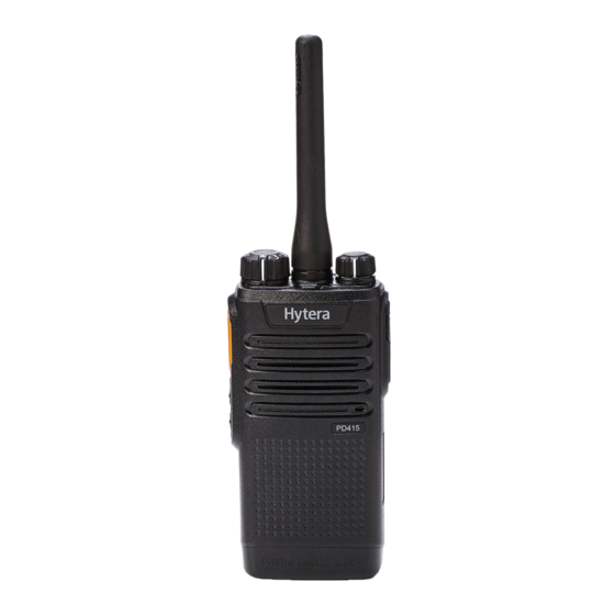
Page 8: Product Controls
VHF1 (136‐174 MHz) Product Controls 1. Product Controls Part Name Part Name ○ ○ PTT (Push-to-Talk) Key Accessory Connector ○ ○ SK1 (Side Key 1) Microphone ○ ○ SK2 (Side Key 2) Battery Latch ○ ○ Channel Selector Knob Antenna ○... -
Page 9: Disassembly And Assembly
VHF1 (136‐174 MHz) Disassembly and Assembly 2. Disassembly and Assembly This section is designed to introduce the way to disassemble the radio. To assemble the radio, do vice versa. Caution Position the waterproof ring into the radio properly during reassembly. ... - Page 10 VHF1 (136‐174 MHz) Disassembly and Assembly Step 4 Remove the two screws on the aluminum chassis. Step 5 Remove the aluminum chassis and the main board. Step 6 Remove the eight screws on the main board. Step 7 Unsolder the soldering joint of the antenna connector and remove the main board.
-
Page 11: Exploded View And Packing Guide
VHF1 (136‐174 MHz) Exploded View and Packing Guide 3. Exploded View and Packing Guide Exploded View Parts list: Part No. Description Qty. Part No. Description 6002448000000 Front Case 6100890100000 Main Waterproof Ring Bracket for PTT O-RING of Code 6002337000000 6100334000000 Key Cover Switch 7400141000000... - Page 12 VHF1 (136‐174 MHz) Exploded View and Packing Guide Part No. Description Qty. Part No. Description 1300D500U0020 Main Board 6001068000010 Code Switch Accessory Connector 7500875000000 Filter Foam 6001978000000 Cover Aluminum 6300269000000 6202121000000 Speaker Fixing Sheet Chassis Waterproof Ring 6101037000000 of Battery 5001210000720 Speaker Connector...
-
Page 13: Packing Guide
VHF1 (136‐174 MHz) Exploded View and Packing Guide Packing Guide... -
Page 14: Specifications
VHF1 (136‐174 MHz) Specifications 4. Specifications General Frequency Range 136‐174 MHz Channel Capacity Channel Spacing 25 kHz/12.5 kHz Operating Voltage 7.4 V (rated) Battery 1500 mAh Li-Ion battery Battery Life (5-5-90 Duty Cycle, High TX Power) Analog: about 12 h High-capacity 1800 mAh Li-Ion Battery Digital: about 16 h Operating Temperature... - Page 15 VHF1 (136‐174 MHz) Specifications Transmitter Power Output 5 W/1 W -36 dBm<1 GHz Spurious Emission -30 dBm>1 GHz ±2.5 kHz @ 12.5 kHz Modulation Limiting ±5.0 kHz @ 25 kHz 40 dB @ 12.5 kHz FM Noise ...
-
Page 16: Circuit Descriptions
VHF1 (136‐174 MHz) Circuit Descriptions 5. Circuit Descriptions Baseband Section 5.1.1 Power Supply Module Diagram of Power Control The power supply employs a single cell 7.4 V Li-ion battery. The RF section uses LDO to generate a 5 V voltage for FGU and PLL circuits, as well as the control parts of TX circuits. The baseband section uses LDO to generate a 3.3 V voltage for Codec, MCU and SCT3928. -
Page 17: Control Module
VHF1 VHF (136‐174 MHz) Circuit Descriptions 5.1.2 Control Module The radio employs the STM32F101VET6(MCU)+SCT3928(Baseband IC) control solution. STM32F101VET6 is the main controller unit (MCU), while SCT3928 is the baseband processor chip, which is used for analog and digital modulation/demodulation, as well as digital voice encoding/decoding. MCU communicates with SCT3928 via HPI BUS and connects to 512K EEPROM via I2C BUS. -
Page 18: Audio Module
VHF1 (136‐174 MHz) Circuit Descriptions 5.1.3 Audio Module Audio Diagram The audio processing section uses SCT3928 and TLV320AIC3204. The audio amplifier uses TDA2822D. The diagram is as follows: These two signals go to FGU for This signal is down converted by modulation RX end and output by BA4116 3V0D... -
Page 19: Rf Section
VHF1 (136‐174 MHz) Circuit Descriptions RF Section 5.2.1 Transmitter Circuit The transmitter circuit is mainly composed of: RF Power Amplifier Circuit Low-pass Filter Circuit (for suppressing harmonics) Auto Power Control (APC) Circuit RF Power Amplifier Circuit The carrier signal (TX signal) generated by TX voltage controlled oscillator (VCO) is modulated and amplified via the buffer amplifier first, then passes through a pre-driver amplifier for primary power amplification. - Page 20 VHF1 (136‐174 MHz) Circuit Descriptions voltage via the sampling resistor and subtracter circuit (composed of the first operational amplifier). This voltage is compared with that of the APC circuit (output by DAC) at the second operational amplifier. Then the error voltage, which is output by the second operational amplifier, controls TX power by controlling the compensated gate bias voltage of the amplifiers (including the driver amplifier and the final-stage amplifier).
-
Page 21: Receiver Circuit
VHF1 (136‐174 MHz) Circuit Descriptions 5.2.2 Receiver Circuit The receiver circuit is mainly composed of RF band-pass filter, low-noise amplifier, mixer, IF filter, IF amplifier and IF processor. S21≤1.5dB Ripple Inband≤ 1dB Stop band attenuation: -30dBc 3V3FGU 3V3dc Lo Amp Low-Noise Amp Lo input level≥7dBm 2SC3356... -
Page 22: Frequency Generation Unit (Fgu)
VHF1 (136‐174 MHz) Circuit Descriptions Receiver Back-end The processed first IF signal is sent to IC BA4116 for second mixing with the second harmonic signal (selected as the second LO signal) of the PLL crystal to get the 450 kHz second IF signal. Then the first IF signal passes through the 450 kHz ceramic filter which filters out the spurious signal before the second IF signal is amplified and frequency-discriminated. - Page 23 VHF1 (136‐174 MHz) Circuit Descriptions VC_TXCO Mod_2 Fc=19.2MHz A=0.1Vpp~2.0Vpp PLL Sky72310 RF feedback LPF 3.0v for core&Vp FGU Close Loop: Compare frequence:4.8MHz Prescaler Level:50~250mVpp S21=-3dB PN: ≤-80 (dBc/Hz)@1KHz Fpass=500MHz PN: ≤-112 (dBc/Hz)@12.5KHz Fstop=800MHz PN: ≤-120 (dBc/Hz)@25KHz Astop=40dB PN: ≤-136 (dBc/Hz)@100KHz PN: ≤-145 (dBc/Hz)@1MHz Two Point modulation:...
-
Page 24: Troubleshooting Flow Chart
VHF1 (136‐174 MHz) Troubleshooting Flow Chart 6. Troubleshooting Flow Chart Control Circuit Check the control circuit Power-on indication is The RF circuit is driven The control circuit normal?[1] normally?[2] is normal. Verify RF power supply circuit (including U302, U303, U306 and U310) and control circuit. -
Page 25: Receiver Circuit
VHF1 (136‐174 MHz) Troubleshooting Flow Chart Receiver Circuit No Receiving Output of Output of 3V3A_RX is 3V3_RX_RF is Check U306 normal?[2] normal?[1] Check Q601 Quiescent operating point of Check Q602 Q602 is normal?[3] Quiescent operating point of Check Q604 Q604 is normal?[4] Input IF signal at Check Z601 to test whether... - Page 26 VHF1 (136‐174 MHz) Troubleshooting Flow Chart Descriptions of normal situation: [1] Output voltage by Q601 Pin 3 is about 3.3 V. [2] Output voltage by U306 Pin 5 or input voltage by Q601 Pin 4 is about 3.3V. [3] Check the collector voltage and base voltage of Q602 when the radio is not receiving. Normally, the base voltage is about 0.7 V, the collector voltage is about 2.7 V and the emitter voltage is 0 V.
-
Page 27: Transmitter Circuit
VHF1 (136 - 174 MHz) Troubleshooting Flow Chart Transmitter Circuit Caution The following tests must be performed under the 7.4 V power supply. No Power Output Power supply Check power supply is normal?[1] circuit TV/APC is Check DAC VGG is normal?[2] normal?[3] output circuit Check 5VRT... - Page 28 VHF1 (136‐174 MHz) Troubleshooting Flow Chart Descriptions of normal situation: [1] Voltage of the power supply is about 7.4 V. [2] For low power, VGG is 1.8 to 2.1 V; for high power, VGG is 2.4 to 2.8 V. [3] For low power, TV/APC is 1 to 1.3 V; for high power, TV/APC is 1.8 to 2.1 V. [4] TX_En is about 3.3 V.
-
Page 29: Fgu Circuit
VHF1 (136‐174 MHz) Troubleshooting Flow Chart FGU Circuit Check FGU circuit Check the 5VFGU, VCC_VCO, power supply 3V3_FGU and circuit 3V3A_FGU_PLL are normal? Q1002, Q1004, Q1005, Replace Q1001 Q1001 and Q1010 are Does VCO oscillate? Q1011 and Q901 are and Q1010 normal?[2] normal?[1] Replace Q1002,... - Page 30 VHF1 (136‐174 MHz) Troubleshooting Flow Chart Descriptions of normal situation: [1] When the radio is transmitting, output voltage by Q1002 Pin 3 is about 4.2 V. When the radio is receiving, output voltage by Q1004 Pin 3 is about 4.2 V. [2] When the radio is transmitting, the emitter voltage, collector voltage and base voltage of Q1010 are about 1.8 V, about 4.18 V and about 2.6 V respectively.
-
Page 31: Interface Definition
VHF1 (136‐174 MHz) Interface Definition 7. Interface Definition Descriptions on J401 and J402 double-pin interface for earpiece, programming and downloading are listed below. Interface Pin No. Signal Illustration SPK- TXD+ J401 SPK+ SPK+ SPK- J402 RXD- OPTEL1... -
Page 32: Tuning Description
VHF1 (136‐174 MHz) Tuning Description 8. Tuning Description Required Test Instruments Radio communication test sets: Aeroflex 3920 and HP8921 Power supply: 3 A/10 V Multimeter Tuner software Tuning Procedures 8.2.1 Tuning the Radio After re-assembling the radio, you need to tune it with the Tuner software. Note The items to be tuned and tuning operations are described in the table below. - Page 33 VHF1 (136‐174 MHz) Tuning Description Item Method Click the “Transmit On” button on Tuner. Adjust the power to the required level as follows: L: 1.2±0.1 W Connect the antenna connector of the radio to the RF port of HP8921, and set HP8921 to TX test mode. Set HP8921 as follows: IF Filter: 230 kHz Filter1: <20 Hz HPF...
- Page 34 VHF1 (136‐174 MHz) Tuning Description Item Method Press the Enter key on the keyboard to confirm your settings. Click the “Transmit Off” button on Tuner. Click the dialog box below LOW_PORT. Select another channel and repeat Step 4 to Step 6. 10.
-
Page 35: Testing The Radio
VHF1 (136‐174 MHz) Tuning Description Item Method Press the Enter key on the keyboard to confirm your settings. Connect the antenna connector of the radio to the RF port of HP8921, and set HP8921 to TX test mode. Receive Oscillator Open the Tuner software and go to “TUNE_DATA ->... - Page 36 VHF1 (136‐174 MHz) Tuning Description Step 5 Check all the tested items on Aeroflex 3920 and make sure they satisfy the following requirements: Frequency Error≤100 Hz Transmit Power: 4.7±0.3 W FSK Error≤5% Magnitude Error≤1% Receiving Performance Step 1 Open the Tuner software and go to “TEST ->...
-
Page 37: Pcb View
9. PCB View Main Board PCB Top Layer... - Page 38 Main Board PCB Bottom Layer...
-
Page 39: Block Diagram
VHF1 (136‐174 MHz) Block Diagram 10. Block Diagram 10.1 Overall Diagram of Radio I2C2 E2PROM BB Processor SCT3928 UART UART1 12.0MHz XTAL OMAP132 SPI2 STM32F101VET6 Security MCLK GPIOs Key Board 12.288MHz GPIOs SW_channel GPIOs GPIOs Audio Codec TLV3204 SPI3 GPIOs Audio preamp preamp... -
Page 40: Block Diagram Of Power Supply Circuit
VHF1 (136‐174 MHz) Block Diagram 10.2 Block Diagram of Power Supply Circuit POW-KEY-DET NTA7002N POWER_ON PWR_ON 3V3D 5VFGU To VCO XC6204F502PR To PLL 5VRT XC6204F502PR To TX 1V2D 3V6D DC-DC DC-DC To Sicomm core ADP2370ACPZ-R7 ADP2370ACPZ-R7 3V3A CODEC RP102N331B 3V3D V_BAT RP102N331B E2PROM... -
Page 41: Block Diagram Of Baseband Circuit
VHF1 (136‐174 MHz) Block Diagram 10.3 Block Diagram of Baseband Circuit 3.6V V_BAT DC-DC 3.6V DC-DC 1.2V 1.2V ADP2370ACPZ-R7 ADP2370ACPZ-R7 RP102N331B 3V3A Fuse POWER SW PLL_CLK EEPROM 7.4VDC PLL_CS PLL_DATA RP102N331B 3V3D PLL_LD FL_Fastlock_Ctrl Pre_Fastlock_Ctrl VCO_H_En RP102N331B 3V3A_RX 12MHZ VCO_L_En STM32F101VET6 TV1\APC EXT_interface... -
Page 42: Block Diagram Of Transmitter Circuit
VHF1 (136‐174 MHz) Block Diagram 10.4 Block Diagram of Transmitter Circuit... -
Page 43: Block Diagram Of Receiver Circuit
VHF1 (136‐174 MHz) Block Diagram 10.5 Block Diagram of Receiver Circuit Low- pass Filter T/ R SW Lo Amp 2SC3356 Lo OSC VC TCXO 19.2 MHz 2SC5108 Low- Noise Amp AT- 41511 BPF2 BPF1 BA4116 Mixer IF Filter IF Processor IF Amp HSMS- 2827 Tuned Voltage... -
Page 44: Block Diagram Of Fgu Circuit
VHF1 (136‐174 MHz) Block Diagram 10.6 Block Diagram of FGU Circuit VC_TXCO F=19.2MHz RF feedback LPF PLL Sky72310 Loop Filter... -
Page 45: Schematic Diagram
Main Processor Circuit 11. Schematic Diagram 主处理器 主处理器 U101 U101 R102 R102 STM32F101VET6 STM32F101VET6 330K-F 330K-F 3V3D R101 R101 R186 R186 HCSN R103 R103 R187 R187 R104 R104 R105 R105 4.7k 4.7k PWR_ON POW-KEY-DET BEEP1 BEEP R188 R188 C102 C102 R106 R106 RFID_IQR... - Page 46 基带处理器+编解码器 Baseband Processor and Codec Circuit 基带处理器和编解码器 L202 L202 3V3A 3V3D1 BLM15PD121SN1 BLM15PD121SN1 R202 R202 C202 C202 C203 C203 R203 R203 3V3D1 0.1u 0.1u R204 R204 U201 U201 SCT3928 SCT3928 L201 L201 C207 NC C207 NC AF-OUT+ HPIDATA0 HPIDATA0 VDDIO33_1 TP205 TP205 3V3D...
- Page 47 Power 电源 电源 V_BAT 5VFGU V_BAT U302 U302 L302 L302 L303 L303 J301 J301 F301 F301 Q301 Q301 Supply XC6204F502PR XC6204F502PR BLM18PG181SN1 BLM18PG181SN1 BLM18PG181SN1 BLM18PG181SN1 BAT-70ADJ3 BAT-70ADJ3 2.5A-32V 2.5A-32V Si2343CD Si2343CD Vout TP302 TP302 C302 0.1u C302 0.1u C304 C304 C305 C305 C306...
- Page 48 Audio Circuit 音频 音频 TP403 TP403 TP404 TP404 TP401 TP401 TP402 TP402 SPK- SPK- SPK+ SPK+ SPK- SPK- SPK+ SPK+ V_BAT L401 3.3uH L401 3.3uH C401 0.1u C401 0.1u C439 C439 C440 C440 C402 C402 C438 C438 C403 C403 J403 J403 AF_OUT- AF_OUT-...
- Page 49 IF Circuit of Receiver 接收中频 接收中频 Z501 Z501 450K 450K 3V3_RX_RF R504 R504 C501 C501 C504 C504 3V3_RX_RF 0.1u 0.1u 0.1u 0.1u C505 C505 0.1u 0.1u L503 L503 560nH 560nH R503 R503 C519 C519 C531 C531 C512 C512 R512 R512 C510 30p C510 30p 0.01u...
- Page 50 Front-end Circuit of Receiver 接收前端 接收前端 3V3_RX_RF Q601 Q601 3V3A_RX EM6M2 EM6M2 L601 L601 R602 100 R602 100 BLM15PD121SN1 BLM15PD121SN1 C601 C601 C602 C602 C603 C603 L609 L609 R601 R601 R603 R603 R604 R604 780nH 780nH 0.1u 0.1u 470p 470p 1000p 1000p RX_En (1)
- Page 51 发射自动控制 Auto Control Circuit of Transmitter 发射自动控制 7V4_PA V_BAT 7V4_PA V_BAT 5V_TX_RF R702 R702 R701 R701 0.1R 0.1R R703 R703 R704 R704 0.1R 0.1R D701 D701 R705 R705 R706 R706 150K 150K 1SS390 1SS390 VDD_OP R707 R707 0.1R 0.1R R708 R708 R709 R709...
- Page 52 Tx Path Circuit 发射通路 发射通路 Q801 Q801 5VRT 5V_TX_RF EM6M2 EM6M2 L801 L801 BLM15PD121SN1 BLM15PD121SN1 C801 C801 C802 C802 R801 R801 0.1u 0.1u 470p 470p TX_En (1,7) C864 C864 470p 470p 5V_TX_RF 3V3D RT801 47k RT801 47k TEM-LEV-DET-TC (1) R802 R802 R803 R803...
- Page 53 PLL Circuit 锁相环 锁相环 3V3_FGU TP901 TP901 3V3A_FGU_PLL PLL_Clk PLL_Clk L901 L901 R901 R901 PLL_Clk TP902 TP902 BLM15PD121SN1 BLM15PD121SN1 C901 C901 C902 C902 PLL_CS PLL_CS C905 C905 C903 C903 C904 C904 PLL_CS 4.7u 4.7u 0.1u 0.1u 470p 470p TP903 TP903 0.1u 0.1u 470p...
- Page 54 FGU Circuit 频率产生单元 频率产生单元 5VFGU EM6M2 Q1002 EM6M2 Q1002 Q1003 Q1003 L1002 L1002 2SC4617 2SC4617 L1003 L1003 VCC_VCO_L VCC_VCO_L BLM15PD121SN1 BLM15PD121SN1 BLM15PD121SN1 BLM15PD121SN1 C1003 C1003 C1002 C1002 R1002 R1002 L1001 L1001 R1003 82K R1003 82K 4.7K 4.7K BLM15PD121SN1 BLM15PD121SN1 R1004 1K R1004 1K 470p 470p...
-
Page 55: Parts List
VHF1 (136‐174 MHz) Parts List 12. Parts List Print Print No. Ref No. Part No. Description No. Ref No. Part No. Description shielding DC_DC shielding B4F 6203698000000 6203697000000 cover cover VCO_BD shielding B3H 6203699000000 6203696000000 shielding cover cover shielding CODEC shielding B2H 6203828000000 6203397000000 cover... - Page 56 VHF1 (136‐174 MHz) Parts List Print Print No. Ref No. Part No. Description No. Ref No. Part No. Description C1050 3101050200010 2pF L309 3221506181000 Ferrite bead C1051 3101011020060 1000pF L310 B5D 3221506181000 Ferrite bead C1052 3101054700010 47pF L311 3221506181000 Ferrite bead C1053 3101061000000 10pF L314...
- Page 57 VHF1 (136‐174 MHz) Parts List Print Print No. Ref No. Part No. Description No. Ref No. Part No. Description C206 T3J 3101071060280 10uF L907 3210306561010 560nH C208 3101051040060 0.1uF L909 3221505121010 Ferrite bead C209 T3J 3101011030050 0.01uF Q1001 B2H 3408002000080 NPN transistor Compound C210 3101054730000 0.047uF...
- Page 58 VHF1 (136‐174 MHz) Parts List Print Print No. Ref No. Part No. Description No. Ref No. Part No. Description C260 B2K 3101014710020 470pF R1014 3001051000000 10Ω C261 T2K 3101011040100 0.1uF R1015 B3H 3001053320010 3.3KΩ C262 T2K 3101014710020 470pF R1016 3001051040000 100KΩ C263 B2K 3101011040100 0.1uF R1017...
- Page 59 VHF1 (136‐174 MHz) Parts List Print Print No. Ref No. Part No. Description No. Ref No. Part No. Description C356 T2K 3101074750000 4.7uF R127 B3K 3001011010080 100Ω C357 T2K 3101051040060 0.1uF R128 3001013300000 33Ω C359 T2F 3101054710010 470pF R129 3001011010080 100Ω C367 T1K 3101052240010 0.22uF R130...
- Page 60 VHF1 (136‐174 MHz) Parts List Print Print No. Ref No. Part No. Description No. Ref No. Part No. Description C505 T4H 3101011040100 0.1uF R187 3001011010080 100Ω C510 T3H 3101053000010 30pF R188 3001011010080 100Ω C512 T2H 3101051040060 0.1uF R189 3001011010080 100Ω C513 T3H 3101012290010 2.2pF R190...
- Page 61 VHF1 (136‐174 MHz) Parts List Print Print No. Ref No. Part No. Description No. Ref No. Part No. Description C655 T4F 3101050500000 5pF R413 T4D 3001054730010 47KΩ C656 B5F 3101056800000 68pF R414 T3G 3001051020000 1KΩ C657 B3G 3101051020010 1000pF R415 T5D 3001050000000 0Ω...
- Page 62 VHF1 (136‐174 MHz) Parts List Print Print No. Ref No. Part No. Description No. Ref No. Part No. Description C851 B1G 3101054710010 470pF R703 T3G 3001050000000 0Ω C852 B1F 3101061800000 18pF R704 3099080398010 0.39Ω C853 B1G 3101052200010 22pF R705 T1G 3001058230000 82KΩ C854 B2G 3101052400010 24pF R706...
- Page 63 VHF1 (136‐174 MHz) Parts List Print Print No. Ref No. Part No. Description No. Ref No. Part No. Description D1009 3304010100180 Varactor R922 3001010000050 0Ω Schottky barrier D101 3301990000030 R923 T1H 3001011020060 1KΩ diode D1010 3304010100220 Varactor R924 3001011030080 10KΩ D1011 3304010100180 Varactor R925...
- Page 64 VHF1 (136‐174 MHz) Parts List Print Print No. Ref No. Part No. Description No. Ref No. Part No. Description Operational D604 B2D 3304010100180 Varactor 1014 U402 3605008005070 amplifier D605 B4E 3304010100180 Varactor 1015 U501 T3H 3603018000000 IF processor IC D606 B4E 3304010100180 Varactor 1016 U601 T3G 3616010000000 Switch IC...
- Page 65 UHF1 (400‐470 MHz)
- Page 66 UHF1 (400‐470 MHz) Contents Contents 1. Product Controls ..........................1 2. Disassembly and Assembly ........................ 2 3. Exploded View and Packing Guide ....................4 3.1 Exploded View ..........................4 3.2 Packing Guide ..........................6 4. Specifications ............................7 5. Circuit Descriptions ..........................9 5.1 Baseband Section..........................
-
Page 67: Product Controls
UHF1 (400‐470 MHz) Product Controls 1. Product Controls Part Name Part Name ○ ○ PTT (Push-to-Talk) Key Accessory Connector ○ ○ SK1 (Side Key 1) Microphone ○ ○ SK2 (Side Key 2) Battery Latch ○ ○ Channel Selector Knob Antenna ○... -
Page 68: Disassembly And Assembly
UHF1 (400‐470 MHz) Disassembly and Assembly 2. Disassembly and Assembly This section is designed to introduce the way to disassemble the radio. To assemble the radio, do vice versa. Caution Position the waterproof ring into the radio properly during reassembly. ... - Page 69 UHF1 (400‐470 MHz) Disassembly and Assembly Step 4 Remove the two screws on the aluminum chassis. Step 5 Remove the aluminum chassis and the main board. Step 6 Remove the eight screws on the main board. Step 7 Unsolder the soldering joint of the antenna connector and remove the main board.
-
Page 70: Exploded View And Packing Guide
UHF1 (400‐470 MHz) Exploded View and Packing Guide 3. Exploded View and Packing Guide Exploded View Parts list: Part No. Description Qty. Part No. Description 6002448000000 Front Case 6100890100000 Main Waterproof Ring Bracket for PTT O-RING of Code 6002337000000 6100334000000 Key Cover Switch 7400141000000... - Page 71 UHF1 (400‐470 MHz) Exploded View and Packing Guide Part No. Description Qty. Part No. Description 1300D500U0020 Main Board 6001068000010 Code Switch Accessory Connector 7500875000000 Filter Foam 6001978000000 Cover Aluminum 6300269000000 6202121000000 Speaker Fixing Sheet Chassis Waterproof Ring 6101037000000 of Battery 5001210000720 Speaker Connector...
-
Page 72: Packing Guide
UHF1 (400‐470 MHz) Exploded View and Packing Guide Packing Guide... -
Page 73: Specifications
UHF1 (400‐470 MHz) Specifications 4. Specifications General Frequency Range 400‐470 MHz Channel Capacity Channel Spacing 25 kHz/12.5 kHz Operating Voltage 7.4 V (rated) Battery 1500 mAh Li-Ion battery Battery Life (5-5-90 Duty Cycle, High TX Power) Analog: about 12 h High-capacity 1800 mAh Li-Ion Battery Digital: about 16 h Operating Temperature... - Page 74 UHF1 (400‐470 MHz) Specifications Transmitter Power Output 4 W/1 W -36 dBm<1 GHz Spurious Emission -30 dBm>1 GHz ±2.5 kHz @ 12.5 kHz Modulation Limiting ±5.0 kHz @ 25 kHz 40 dB @ 12.5 kHz FM Noise ...
-
Page 75: Circuit Descriptions
UHF1 (400‐470 MHz) Circuit Descriptions 5. Circuit Descriptions Baseband Section 5.1.1 Power Supply Module Diagram of Power Control The power supply employs a single cell 7.4 V Li-ion battery. The RF section uses LDO to generate a 5 V voltage for FGU and PLL circuits, as well as the control parts of TX circuits. The baseband section uses LDO to generate a 3.3 V voltage for Codec, MCU and SCT3928. -
Page 76: Control Module
UHF1 (400‐470 MHz) Circuit Descriptions 5.1.2 Control Module The radio employs the STM32F101VET6(MCU)+SCT3928(Baseband IC) control solution. STM32F101VET6 is the main controller unit (MCU), while SCT3928 is the baseband processor chip, which is used for analog and digital modulation/demodulation, as well as digital voice encoding/decoding. MCU communicates with SCT3928 via HPI BUS and connects to 512K EEPROM via I2C BUS. -
Page 77: Audio Module
UHF1 (400‐470 MHz) Circuit Descriptions 5.1.3 Audio Module Audio Diagram The audio processing section uses SCT3928 and TLV320AIC3204. The audio amplifier uses TDA2822D. The diagram is as follows: These two signals go to FGU for This signal is down converted by modulation RX end and output by BA4116 3V0D... -
Page 78: Rf Section
UHF1 (400‐470 MHz) Circuit Descriptions RF Section 5.2.1 Transmitter Circuit The transmitter circuit is mainly composed of: RF Power Amplifier Circuit Low-pass Filter Circuit (for suppressing harmonics) Auto Power Control (APC) Circuit RF Power Amplifier Circuit The carrier signal (TX signal) generated by TX voltage controlled oscillator (VCO) is modulated and amplified via the buffer amplifier first, then passes through a pre-driver amplifier for primary power amplification. - Page 79 UHF1 (400‐470 MHz) Circuit Descriptions voltage via the sampling resistor and subtracter circuit (composed of the first operational amplifier). This voltage is compared with that of the APC circuit (output by DAC) at the second operational amplifier. Then the error voltage, which is output by the second operational amplifier, controls TX power by controlling the compensated gate bias voltage of the amplifiers (including the driver amplifier and the final-stage amplifier).
-
Page 80: Receiver Circuit
UHF1 (400‐470 MHz) Circuit Descriptions 5.2.2 Receiver Circuit The receiver circuit is mainly composed of RF band-pass filter, low-noise amplifier, mixer, IF filter, IF amplifier and IF processor. S21≤1.5dB Ripple Inband≤ 1dB Stop band attenuation: -30dBc 3V3FGU 3V3dc Lo Amp Low-Noise Amp Lo input level≥7dBm 2SC3356... -
Page 81: Frequency Generation Unit (Fgu)
UHF1 (400‐470 MHz) Circuit Descriptions Receiver Back-end The processed first IF signal is sent to IC BA4116 for second mixing with the third harmonic signal (selected as the second LO signal) of the PLL crystal to get the 450 kHz second IF signal. Then the first IF signal passes through the 450 kHz ceramic filter which filters out the spurious signal before the second IF signal is amplified and frequency-discriminated. - Page 82 UHF1 (400‐470 MHz) Circuit Descriptions VC_TXCO Mod_2 Fc=19.2MHz A=0.1Vpp~2.0Vpp PLL Sky72310 RF feedback LPF 3.0v for core&Vp FGU Close Loop: Compare frequence:4.8MHz Prescaler Level:50~250mVpp S21=-3dB PN: ≤-80 (dBc/Hz)@1KHz Fpass=500MHz PN: ≤-112 (dBc/Hz)@12.5KHz Fstop=800MHz PN: ≤-120 (dBc/Hz)@25KHz Astop=40dB PN: ≤-136 (dBc/Hz)@100KHz PN: ≤-145 (dBc/Hz)@1MHz Two Point modulation:...
-
Page 83: Troubleshooting Flow Chart
UHF1 (400‐470 MHz) Troubleshooting Flow Chart 6. Troubleshooting Flow Chart Control Circuit Check the control circuit Power-on indication is The RF circuit is driven The control circuit normal?[1] normally?[2] is normal. Verify RF power supply circuit (including U302, U303, U306 and U310) and control circuit. -
Page 84: Receiver Circuit
UHF1 (400‐470 MHz) Troubleshooting Flow Chart Receiver Circuit No Receiving Output of Output of 3V3A_RX is 3V3_RX_RF is Check U306 normal?[2] normal?[1] Check Q601 Quiescent operating point of Check Q602 Q602 is normal?[3] Quiescent operating point of Check Q604 Q604 is normal?[4] Input IF signal at Check Z601 to test whether... - Page 85 UHF1 (400‐470 MHz) Troubleshooting Flow Chart Descriptions of normal situation: [1] Output voltage by Q601 Pin 3 is about 3.3 V. [2] Output voltage by U306 Pin 5 or input voltage by Q601 Pin 4 is about 3.3V. [3] Check the collector voltage and base voltage of Q602 when the radio is not receiving. Normally, the base voltage is about 0.7 V, the collector voltage is about 2.7 V and the emitter voltage is 0 V.
-
Page 86: Transmitter Circuit
UHF1 (400‐470 MHz) Troubleshooting Flow Chart Transmitter Circuit Caution The following tests must be performed under the 7.4 V power supply. No Power Output Power supply Check power supply is normal?[1] circuit TV/APC is Check DAC VGG is normal?[2] normal?[3] output circuit Check 5VRT 5V_TX_RF is... - Page 87 UHF1 (400‐470 MHz) Troubleshooting Flow Chart Descriptions of normal situation: [1] Voltage of the power supply is about 7.4 V. [2] For low power, VGG is 1.8 to 2.1 V; for high power, VGG is 2.4 to 2.8 V. [3] For low power, TV/APC is 1 to 1.3 V; for high power, TV/APC is 1.8 to 2.1 V. [4] TX_En is about 3.3 V.
-
Page 88: Fgu Circuit
UHF1 (400‐470 MHz) Troubleshooting Flow Chart FGU Circuit Check FGU circuit Check the 5VFGU, VCC_VCO, power supply 3V3_FGU and circuit 3V3A_FGU_PLL are normal? Q1002, Q1004, Q1005, Replace Q1001 Q1001 and Q1010 are Does VCO oscillate? Q1011 and Q901 are and Q1010 normal?[2] normal?[1] Replace Q1002,... - Page 89 UHF1 (400‐470 MHz) Troubleshooting Flow Chart Descriptions of normal situation: [1] When the radio is transmitting, output voltage by Q1004 Pin 3 is about 4.2 V. When the radio is receiving, output voltage by Q1002 Pin 3 is about 4.2 V. [2] When the radio is transmitting, the emitter voltage, collector voltage and base voltage of Q1010 are about 1.8 V, about 4.18 V and about 2.6 V respectively.
-
Page 90: Interface Definition
UHF1 (400‐470 MHz) Interface Definition 7. Interface Definition Descriptions on J401 and J402 double-pin interface for earpiece, programming and downloading are listed below. Interface Pin No. Signal Illustration SPK- TXD+ J401 SPK+ SPK+ SPK- J402 RXD- OPTEL1... -
Page 91: Tuning Description
UHF1 (400‐470 MHz) Tuning Description 8. Tuning Description Required Test Instruments Radio communication test sets: Aeroflex 3920 and HP8921 Power supply: 3 A/10 V Multimeter Tuner software Tuning Procedures 8.2.1 Tuning the Radio After re-assembling the radio, you need to tune it with the Tuner software. Note The items to be tuned and tuning operations are described in the table below. - Page 92 UHF1 (400‐470 MHz) Tuning Description Item Method Click the “Transmit On” button on Tuner. Adjust the power to the required level as follows: L: 1.2±0.1 W Connect the antenna connector of the radio to the RF port of HP8921, and set HP8921 to TX test mode. Set HP8921 as follows: IF Filter: 230 kHz Filter1: <20 Hz HPF...
- Page 93 UHF1 (400‐470 MHz) Tuning Description Item Method Press the Enter key on the keyboard to confirm your settings. Click the “Transmit Off” button on Tuner. Click the dialog box below LOW_PORT. Select another channel and repeat Step 4 to Step 6. 10.
-
Page 94: Testing The Radio
UHF1 (400‐470 MHz) Tuning Description Item Method Press the Enter key on the keyboard to confirm your settings. Connect the antenna connector of the radio to the RF port of HP8921, and set HP8921 to TX test mode. Receive Oscillator Open the Tuner software and go to “TUNE_DATA ->... - Page 95 UHF1 (400‐470 MHz) Tuning Description Step 5 Check all the tested items on Aeroflex 3920 and make sure they satisfy the following requirements: Frequency Error≤100 Hz Transmit Power: 4.2±0.3 W FSK Error≤5% Magnitude Error≤1% Receiving Performance Step 1 Open the Tuner software and go to “TEST ->...
-
Page 96: Pcb View
9. PCB View Main Board PCB Top Layer... - Page 97 Main Board PCB Bottom Layer...
-
Page 98: Block Diagram
UHF1 (400‐470 MHz) Block Diagram 10. Block Diagram 10.1 Overall Diagram of Radio I2C2 E2PROM BB Processor SCT3928 UART UART1 12.0MHz XTAL OMAP132 SPI2 STM32F101VET6 Security MCLK GPIOs Key Board 12.288MHz GPIOs SW_channel GPIOs GPIOs Audio Codec TLV3204 SPI3 GPIOs Audio preamp preamp... -
Page 99: Block Diagram Of Power Supply Circuit
UHF1 (400‐470 MHz) Block Diagram 10.2 Block Diagram of Power Supply Circuit POW-KEY-DET NTA7002N POWER_ON PWR_ON 3V3D 5VFGU To VCO XC6204F502PR To PLL 5VRT XC6204F502PR To TX 1V2D 3V6D DC-DC DC-DC To Sicomm core ADP2370ACPZ-R7 ADP2370ACPZ-R7 3V3A CODEC RP102N331B 3V3D V_BAT RP102N331B E2PROM... -
Page 100: Block Diagram Of Baseband Circuit
UHF1 (400‐470 MHz) Block Diagram 10.3 Block Diagram of Baseband Circuit 3.6V V_BAT DC-DC 3.6V DC-DC 1.2V 1.2V ADP2370ACPZ-R7 ADP2370ACPZ-R7 RP102N331B 3V3A Fuse POWER SW PLL_CLK EEPROM 7.4VDC PLL_CS PLL_DATA RP102N331B 3V3D PLL_LD FL_Fastlock_Ctrl Pre_Fastlock_Ctrl VCO_H_En RP102N331B 3V3A_RX 12MHZ VCO_L_En STM32F101VET6 TV1\APC EXT_interface... -
Page 101: Block Diagram Of Transmitter Circuit
UHF1 (400‐470 MHz) Block Diagram 10.4 Block Diagram of Transmitter Circuit... -
Page 102: Block Diagram Of Receiver Circuit
UHF1 (400‐470 MHz) Block Diagram 10.5 Block Diagram of Receiver Circuit Low- pass Filter T/ R SW Lo Amp 2SC3356 Lo OSC VC TCXO 19.2 MHz 2SC5108 Low- Noise Amp AT- 41511 BPF2 BPF1 BA4116 Mixer IF Filter IF Processor IF Amp HSMS- 2827 Tuned Voltage... -
Page 103: Block Diagram Of Fgu Circuit
UHF1 (400‐470 MHz) Block Diagram 10.6 Block Diagram of FGU Circuit VC_TXCO F=19.2MHz RF feedback LPF PLL Sky72310 Loop Filter... -
Page 104: Schematic Diagram
Main Processor Circuit 主处理器 主处理器 11. Schematic Diagram U101 U101 R102 R102 STM32F101VET6 STM32F101VET6 330K-F 330K-F 3V3D R101 R101 R186 R186 HCSN R103 R103 R187 R187 PWR_ON POW-KEY-DET R188 R188 C102 C102 R106 R106 RFID_IQR PA2/USART2_TX R107 R107 R189 R189 150K-F 150K-F PLLSEL... - Page 105 Baseband Processor and Codec Circuit 基带处理器和编解码器 基带处理器和编解码器 L202 L202 3V3A BLM15PD121SN1 BLM15PD121SN1 R202 R202 3V3A C202 C202 C203 C203 R203 R203 3V3D1 0.1u 0.1u R204 R204 U201 U201 SCT3928 SCT3928 L201 L201 C207 1u C207 1u AF-OUT+ HPIDATA0 HPIDATA0 VDDIO33_1 TP205 TP205 3V3D...
- Page 106 Power 电源 电源 V_BAT 5VFGU V_BAT U302 U302 L302 L302 L303 L303 Supply J301 J301 F301 F301 Q301 Q301 XC6204F502PR XC6204F502PR BLM18PG181SN1 BLM18PG181SN1 BLM18PG181SN1 BLM18PG181SN1 BAT-70ADJ3 BAT-70ADJ3 2.5A-32V 2.5A-32V Si2343CD Si2343CD Vout TP302 TP302 C302 0.1u C302 0.1u C304 C304 C305 C305 C306...
- Page 107 Audio Circuit 音频 音频 TP403 TP403 TP404 TP404 TP401 TP401 TP402 TP402 SPK- SPK- SPK+ SPK+ SPK- SPK- SPK+ SPK+ V_BAT L401 3.3uH L401 3.3uH C401 0.1u C401 0.1u C439 C439 C440 C440 C402 C402 C438 C438 C403 C403 J403 J403 Q401 Q401...
- Page 108 IF Circuit of Receiver 接收中频 接收中频 Z501 Z501 450K 450K 3V3_RX_RF R504 R504 C501 C501 C504 C504 3V3_RX_RF 0.1u 0.1u 0.1u 0.1u C505 C505 0.1u 0.1u L503 L503 330nH 330nH R503 R503 C519 C519 C531 C531 C512 C512 R512 R512 C510 22p C510 22p 0.01u...
- Page 109 Front-end Circuit of Receiver 接收前端 接收前端 3V3_RX_RF Q601 Q601 3V3A_RX EM6M2 EM6M2 L601 L601 R602 68 R602 68 BLM15PD121SN1 BLM15PD121SN1 C601 C601 C602 C602 C603 C603 L609 L609 R601 R601 R603 R603 R604 R604 100nH 100nH 0.1u 0.1u 470p 470p 1000p 1000p RX_En (1)
- Page 110 Auto Control Circuit of Transmitter 发射自动控制 发射自动控制 7V4_PA V_BAT 7V4_PA V_BAT 5V_TX_RF R702 R702 R701 R701 0.1R 0.1R R703 R703 R704 R704 0.1R 0.1R D701 D701 R705 R705 R706 R706 390K 390K 1SS390 1SS390 VDD_OP R707 R707 0.1R 0.1R R708 R708 R709 R709...
- Page 111 Tx Path Circuit 发射通路 发射通路 Q801 Q801 5VRT 5V_TX_RF EM6M2 EM6M2 L801 L801 BLM15PD121SN1 BLM15PD121SN1 C801 C801 C802 C802 R801 R801 0.1u 0.1u 470p 470p TX_En (1,7) C864 C864 470p 470p 5V_TX_RF 3V3D RT801 47k RT801 47k TEM-LEV-DET-TC (1) R802 R802 R803 R803...
- Page 112 PLL Circuit 锁相环 锁相环 3V3_FGU TP901 TP901 3V3A_FGU_PLL PLL_Clk PLL_Clk L901 L901 R901 R901 PLL_Clk TP902 TP902 BLM15PD121SN1 BLM15PD121SN1 C901 C901 C902 C902 PLL_CS PLL_CS C905 C905 C903 C903 C904 C904 PLL_CS 4.7u 4.7u 0.1u 0.1u 470p 470p TP903 TP903 0.1u 0.1u 470p...
- Page 113 FGU Circuit 频率产生单元 频率产生单元 5VFGU EM6M2 Q1002 EM6M2 Q1002 Q1003 Q1003 L1002 L1002 2SC4617 2SC4617 L1003 L1003 VCC_VCO_L VCC_VCO_L BLM15PD121SN1 BLM15PD121SN1 BLM15PD121SN1 BLM15PD121SN1 C1003 C1003 C1002 C1002 R1002 R1002 L1001 L1001 R1003 82K R1003 82K 4.7K 4.7K BLM15PD121SN1 BLM15PD121SN1 R1004 1K R1004 1K 470p 470p...
-
Page 114: Parts List
UHF1 (400‐470 MHz) Parts List 12. Parts List Print Print No. Ref No. Part No. Description Ref No. Part No. Description shielding B4F 6203698000000 D804 B2C 3399030000010 PIN diode cover VCO_BD Schottky barrier B3H 6203699000000 D901 3301990000030 shielding cover diode shielding Schottky barrier... - Page 115 UHF1 (400‐470 MHz) Parts List Print Print No. Ref No. Part No. Description Ref No. Part No. Description C1044 3101050590020 0.5pF L301 3221506181000 Ferrite bead C1045 3101050600010 6pF L302 T1H 3221506181000 Ferrite bead C1046 3101060400010 4pF L303 T2H 3221506181000 Ferrite bead C1049 3101060400010 4pF L304...
- Page 116 UHF1 (400‐470 MHz) Parts List Print Print No. Ref No. Part No. Description Ref No. Part No. Description C203 T3J 3101071060010 10uF L903 3221505121010 Ferrite bead C206 T3J 3101071060010 10uF L904 3221505121010 Ferrite bead C208 3101051040060 0.1uF L905 3221505121010 Ferrite bead C209 T3J 3101011030050 0.01uF L906...
- Page 117 UHF1 (400‐470 MHz) Parts List Print Print No. Ref No. Part No. Description Ref No. Part No. Description C259 B2J 3101011040090 0.1uF R1010 3001014730010 47KΩ C260 B2K 3101014710020 470pF R1011 B2H 3001062210000 220Ω C261 T2K 3101011040090 0.1uF R1012 B3H 3001053910010 390Ω C262 T2K 3101014710020 470pF R1013...
- Page 118 UHF1 (400‐470 MHz) Parts List Print Print No. Ref No. Part No. Description Ref No. Part No. Description C355 T3K 3101052710000 270pF R131 3001011010080 100Ω C356 T2K 3101074750000 4.7uF R132 B5K 3001014720050 4.7KΩ C357 T2K 3101051040060 0.1uF R133 3001014720050 4.7KΩ C359 T2F 3101054710010 470pF R134...
- Page 119 UHF1 (400‐470 MHz) Parts List Print Print No. Ref No. Part No. Description Ref No. Part No. Description C501 T4H 3101011040100 0.1uF R191 B3K 3001051520000 1.5KΩ C504 T3H 3101011040100 0.1uF R192 B3K 3001011530010 15KΩ C505 T4H 3101011040100 0.1uF R193 B3K 3001011530010 15KΩ C510 T3H 3101051800010 18pF R194...
- Page 120 UHF1 (400‐470 MHz) Parts List Print Print No. Ref No. Part No. Description Ref No. Part No. Description C653 T3F 3101011040090 0.1uF R417 3001051010040 100Ω C654 T3G 3101051500020 15pF R418 3001051030050 10KΩ C655 T4F 3101056890000 6.8pF R419 3001051030050 10KΩ C656 B5F 3101058200000 82pF R420 3001052240000 220KΩ...
- Page 121 UHF1 (400‐470 MHz) Parts List Print Print No. Ref No. Part No. Description Ref No. Part No. Description C852 B1F 3101061300000 13pF R715 T2G 3001051040000 100KΩ C853 B1G 3101052200010 22pF R717 T2G 3001050000000 0Ω C854 B2G 3101052400010 24pF R718 T2G 3001051050000 1MΩ C857 B2G 3101052700000 27pF R719...
- Page 122 UHF1 (400‐470 MHz) Parts List Print Print No. Ref No. Part No. Description Ref No. Part No. Description D1005 B1H 3304010100220 Varactor RN103 B4K 3005051010010 100Ω D1006 B3H 3303030800020 Switching diode RN104 3005051010010 100Ω D1007 3304010100890 Varactor RN105 3005051010010 100Ω D1008 B3G 3399030000010 PIN diode RN106...
- Page 123 UHF1 (400‐470 MHz) Parts List Print Print No. Ref No. Part No. Description Ref No. Part No. Description (super Baseband D109 T3B 3307110100080 U201 B2K 3613999000150 green) processor IC protection D110 T1F 3399040600000 U202 3606010000070 D/A conversion IC diode protection D301 T3E 3399040600000 U203...
- Page 124 Hytera Communications Corporation Limited. 2015 Hytera Communications Corporation Limited. 1616300000520 2015 06 24 L07157...
Need help?
Do you have a question about the PD415 and is the answer not in the manual?
Questions and answers