
Related Manuals for Samsung SF-4700


Summary of Contents for Samsung SF-4700
-
Page 1: Table Of Contents
SAMSUNG FACSIMILE SF-4700 SERVICE Manual FACSIMILE CONTENTS 1. Precautions 2. Specifications 3. Installations 4. Disassembly 5. List of Abbreviations 6. Circuit Descriptions 7. Troubleshooting 8. Exploded Views & Parts List 9. Electrical Parts List 10. Connection Diagrams 11. Pcb Diagrams... - Page 2 ELECTRONICS © Samsung Electronics Co.,Ltd. JUNE 2000 Printed in Korea. VERSION NO. : 2.00 P/N.: JB-0002A...
-
Page 3: Precautions
6. Observe the original lead dress, especially near sharp edges, AC, and high voltage power supplies. Always inspect for pinched, out-of-place, or frayed wiring. Do not change the spacing between components and the printed circuit board. Samsung Electronics... - Page 4 ESDs. Normal motions, such as the brushing together of 3. Use only a grounded tip soldering iron to solder or clothing fabric and lifting one’s foot from a desolder ESDs. carpeted floor, can generate static electricity sufficient to damage an ESD. Samsung Electronics...
-
Page 5: Specifications
Host Based Printing (GDI) Printer Driver Windows 98/2000 Driver Inter Face IEEE1284 2-2 Head Babbage mono standard Birch color Print Head 208 nozzles 192 nozzles Ink type Pigment Ink Color Black Color Ink Yield about 600 sh. about 200 sh. Samsung Electronics... - Page 6 0.5 Mbyte user memory Capacity (*3) Back-up Time 15 sec (Continuous Power Failure) MEMORY Confidential Forced Memory Tx. Memory Rx. Automatic reception when paper empty. (*3) Monochromatic CCITT NO. 1 CHART can be saved by 80 sheets per 1.0M Byte. Samsung Electronics...
- Page 7 Multipage Copy Upto 99 Pages Gray Scale 256 Levels COPY Reduction & 25%~200% Enlargement (Reference is the top center of Document) Answering I/F TEL I/F Ext. Phone 1-jack, Extension Phone Transfer Sensors Paper Jam OTHERS Real Time Clock Samsung Electronics...
- Page 8 Dimensions (W T D T H) 235 mm Weight 6.9Kg 2-6 Accessaries Tel Line Power Cord FAX Driver 1 CD - ROM Ink Cartridge INK-M50 (MONO) 1EA, INK-C60 (COLOR) 1EA Manual Carrier Sheet Yes (with Tick Mark : A5 Size) Samsung Electronics...
-
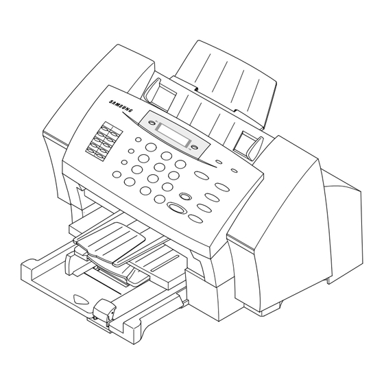
Page 9: Installations
Extender ocument exit tray 3-3 Telephone Line Plug one end of the telephone line cord into the TEL LINE jack and the other end into a standard phone wall jack. Samsung Electronics... - Page 10 3-4. If you want to turn it off, unplug the power cord. Note : If documents are deleted from memory due to a power failure, the machine automatically prints out a Power failure report after power is supplied. Samsung Electronics...
- Page 11 2. If you are replacing used cartridges, remove the old cartridges. 5. Insert the print cartridges in the carrier. Press SETUP,MENU & START button. Pull the print cartridges handle toward you until you hear a click, then remove the print cartridges. Cartridge handle Samsung Electronics...
-
Page 12: Disassembly
2. Push the bushing on both ends of the roller the roller is heavily worn, replace it with a slightly inward, then rotate it until it reaches the new one. slot as shown below. Then lift the roller out. Bushing White roller Control panel Samsung Electronics... - Page 13 4-3 Top Cover Ass’y 1. Lift the control panel and open the print cartridge compartment cover. Remove the white roller ass’y. Remove the six screws shown below. Cartridge compartment cover Control panel 2. Remove the three screws shown below. Samsung Electronics...
- Page 14 Disassembly 3. Open the outer guide. Outer guide Outer guide 4. Take out the top cover ass’y. Top cover ass’y Top cover ass’y 5. Remove the two screws securing the speaker. Samsung Electronics...
- Page 15 2. Remove the drive roller as described in ‘4-4-1 alcohol. If it is heavily stained or scratched, Rollers’. replace it with a new one. 3. Remove the one screw securing the CIS ass’y and unplug the CIS harness. Take out the CIS ass’y. Samsung Electronics...
- Page 16 2. Unplug the motor connector from the main PBA. Make sure the harness is released from one hooks securing the harness as shown below. Main PBA Hook Scan motor ass’y 4. Remove the two screws securing the motor to the Motor harness motor bracket. Motor bracket Samsung Electronics...
- Page 17 2. Unplug the SMPS connector from the Main PBA. Make sure the harness is released from the hook as shown below. Hook SMPS connector SMPS 3. Remove the one screw securing the ground wires to the parallel unit as shown. SMPS ground wire LIU ground wire Samsung Electronics...
- Page 18 2. Remove the one screw securing the ground wires to the parallel unit. SMPS ground wire LIU ground wire 5. Pulling the snap fits locking the PBA outward, push up the LIU PBA. 3. Unplug the LIU connector from the Main PBA. Samsung Electronics...
- Page 19 2. Unplug the one connector and remove two screw the Main PBA. shown below, and take out the Parallel Unit. 3. Remove the two screws as shown below and take out the Scan Lawer Frame. Scan lawer frame Parallel unit Parallel harness Samsung Electronics...
- Page 20 – Top Cover Ass’y (see page 4-3) – SMPS (see page 4-6) – LIU PBA (see page 4-7) – Parallel Unit (see page 4-8) 2. Remove the two screws as shown below and take out the SMPS Frame. SMPS frame ASF cassette ass’y Samsung Electronics...
- Page 21 • Clean the surface of the rubber pad with ethyl alco- hol. After wiping it, be sure to dry it. Check the rubber wear. If the wear reaches 1/2 its original thickness, replace it with a new one. 4-10 Samsung Electronics...
- Page 22 OPE unit 3. Turn the upper scan frame of the OPE Unit over. 4. Remove the three screws and take out the spring pinch. Then take out the roll pinch. Spring pinch Roll pinch Upper scan frame Samsung Electronics 4-11...
- Page 23 • When you reassemble the PBA, secure the screws according in the order of the number printed on the PBA. • After reassembling, operate the machine to make sure it works properly. • After reassembling, make sure the LCD is not blocked. 4-12 Samsung Electronics...
- Page 24 4. Pull the sensor lever towards you and take out the Main PBA. Main PBA Main PBA Sensor lever Door open Motor Sensor Motor Speaker Motor Paper Sensor Print Head SMPS Parallel Unit Note: When you reassemble the unit, do not pinch or short the wire harness. Samsung Electronics 4-13...
- Page 25 2. Take out FRC cable from the main PBA, take out 2 the ass’y in the direction of arrow. CR springs that fix CR shaft, and then separate carriage Assembly. CR shaft FPC cable Home ass’y Carriage ass’y 4-14 Samsung Electronics...
- Page 26 – Home Ass’y (see page 4-14) – Carriage Ass’y (see page 4-14) 2. Remove the friction ass’y, then take out the Holder roller actuator feed. Actuator feed Friction ass’y 4. Pull out the base frame ass’y. Base frame ass’y Samsung Electronics 4-15...
- Page 27 2. Remove the bearing feed from the main frame. Pull 2. Remove the two screws and take out the LF brack- the feeder roller in the direction of arrow and take et ass’y. it out. LF bracket ass’y Feed roller Bearing feed 4-16 Samsung Electronics...
-
Page 28: List Of Abbreviations
MULTI FUNCTION Peripheral INTERFACE UART Universal Asynchronous Receiver/Transmitter Extended Capabilities Port CARRIAGE RETURN LINE FEED SCANIP SCAN IMAGE PROCESSOR CONTACT IMAGE SENSOR ANALOG TO DIGITAL DIGITAL TO ANALOG Line Interface Unit Transformer Input from Transformer Receive Output Transformer Line Input Samsung Electronics... - Page 29 HOE1~HOE16 VBUS /USB-RST PRINT CML_ON /USB-CS USBDP CONTROL/ /DRAM_EN /FAULT-TEST CIRCUIT /USB-XDDCK USBDM ICML1 Controller BIASOFF /USB-XDREQ PREHEAT _M PREHEAT _C /USB-INT PULLUP GLED 48MHz CLK RLED BLED Fig.6-1-1. Entire Structure of Main Circuit for Each Key Signal Samsung Electronics...
- Page 30 - 16bit data bus MCLK(38MHz) and become LOW ACTIVE. These signals are strobe signals used to read and • A0 - A17 write data when each CHIP SELECT is connected - ADDRESS BUS (A18 - A21 are reserved.) Samsung Electronics...
- Page 31 1-2) KS32C6400 has 2 UART channels. The baud rate Receiver/Transmitter) at KS32C6400 enables the main is 9600bps. and OPE to transmit serial UART Block IR Tx IR Rx Encoder Decoder Fig.6-1-2. UART BLOCK DIAGRAM TXD : START STOP RXD : START STOP Fig.6-1-3 UART DATA FORMAT Samsung Electronics...
- Page 32 STROBE (/WR) in order to move this data into DMA ACKNOWLEDGE signal and drives DMA destination memory, and then stores the data. channel 0 to produce CHIP SELECT and READ STROBE (/RD) at the external MCLK /XDREQ /XDACK D[15:0] Fig.6-1-4 EXTERNAL DMA TIMING DIAGRAM Samsung Electronics...
- Page 33 BYTE/HALF WORD ACCESS supports EDO DRAM nected with up to 1M - 4M halfword, two (2) of 512 as well as normal DRAM. DRAM READ/WRITE sig- Kbytes are nals are /RD and /WR signals used to control system connected for this product. Samsung Electronics...
- Page 34 EN, and BIASOFF, and consists of signals to check the each signal. status of the head, HEAD-DATA. Fire Enable Timer /HGA Signal (PD) Pre-Heat Pulse Width Fire Pulse Width Signal Front End Delay Pr-Heat Delay Width Back End Delay Fig.6-1-5 Timing Diagram to Drive Head Samsung Electronics...
- Page 35 It controls CR (Carriage Return) motor used to print documents and LF (Line Feed) motor used to feed and eject paper. CR motor controller can support 75, 150, 200, 300, 600, or 1200dpi according to resolution, while LF Samsung Electronics...
- Page 36 GIOP3/nTRST /MODEM_RST RESET OFF RESET ON GIOP4/TDO RECALL RECALL ON RECALL OFF:IDLE STATE GIOP5 /M_HEAD_EN DISABLE MONO PRINT HEAD ENABLE MONO PRINT HEAD GIOP6 /USB_RST RESET OFF:IDLE STATE RESET ON GIOP7/nWAIT RX_CTL RX LINE TX LINE OR REMOTE Samsung Electronics...
- Page 37 KS32C6400 are reset as well. XC61FN4512 output output terminal becomes low (0V) and the voltage is terminal of open drain structure is pulled up 1MΩ impressed to flash memory and KS32C6400, run- and put out. ning RESET (LOW ACTIVE). Flash memory and Samsung Electronics...
- Page 38 Pixel Data Sample Clock Scanner Control Image Converter Controller Processor Module Analog Digitized Processed Data Data Data Data Timing Formatted Data for DMA System Data BUS Control SCANIP Control Data Data Memory Controller Fig.6-1-8 SCANIP Block Diagram Samsung Electronics 6-10...
- Page 39 – Color CIS (Canon, Dyna, Toshiba) interface – Automatic Motor Control – Image Processing Mode : TIP, Ordered dither, Error diffusion – 256 Gray Scale – AGC function – PC Gray Scan function g External SRAM: 32Kbyte, 15Ns Access Time Samsung Electronics 6-11...
- Page 40 COLOR PRINTHEAD ID DATA : SERIAL HEX CODE : 08H GIOP 12 /SPK_CTL AUDIO AMP. OFF AUDIO AMP. ON GIOP 13 AMB_TEMP BI-DIRECTION DATA TRANSFER TO FROM DIGITAL THERMOMETER GIOP 14 M_HEADDATA MONO PRINTHEAD ID DATA : SERIAL HEX CODE : 07H GIOP 15 Samsung Electronics 6-12...
- Page 41 In 1200dpi (in case of Head: 12KHz) mode, timing period is 2.6usec (1/1200÷16 groups). The signal put in each driver(window time) is active “L”, with the biggest driver current max 100mA and output voltage +11.75V. Samsung Electronics 6-13...
- Page 42 (8bit) BP16 (CP16) Mono CONTROLLER /FAULT-TEST Color Fault (Short) Test /FAULT BIASOFF BS1 (CS1) Head HEAD-DATA Detection HSC,HSM Head /M_HEAD_EN, /C_HEAD_EN) Selector OK2PRINT Substrate BH1 (CH1) SCANIP (U29) PRE-HEAT Heat IMAGE PROCESSOR Fig.6-1-9 Block Diagram of Printer Samsung Electronics 6-14...
- Page 43 FAULT-TEST output “L” to detect fault of +11.75V. the head, +22V gets off. If the head is in a short (LOW), when the level of “/FAULT-TEST” signal Mono Head 70°C 35°C Pre-Heat if below 35°c Fig.6-1-10. Temperature around Mono Head Samsung Electronics 6-15...
- Page 44 Min 500ns Clock Delay(Min 500ns) C_HEADDATA or M_HEAD DATA bit7 bit6 bit5 bit4 bit3 bit2 bit1 bit0 Head I.D read : HEAD-DATA (Clock 1,2=50~500KHz). Mono : 07H Color : ICH Photo : 09H Fig.6-1-12. HEAD DETECTION TIMING DIAGRAM Samsung Electronics 6-16...
- Page 45 (+11.75V). It is depicted in the following diagram. Fire Enable Timer (PD) Signal Pre-Heat Pulse Width Fire Pulse Width Signal Front End Delay Back End Delay Pre-Heat Delay Width Fig.6-1-13. HEAD DRIVING TIMING DIAGRAM Samsung Electronics 6-17...
- Page 46 Circuit HSC or HSM BA10 BA11 BA12 BA13 BP1- BP16 (Tp) Fig.6-1-14. TIMING DIAGRAM FOR EACH NOZZLE Samsung Electronics 6-18...
- Page 47 Circuit 6-1-5-5. INK CARTRIDGE • PIN ARRAY OF MONO INK CARTRIDGE There are 208 heater chips in mono ink cartridge. Address (BA1_ ~ BA13_) Column Data(BPx) Samsung Electronics 6-19...
- Page 48 • PIN ARRAY OF COLOR INK CARTRIDGE There are 192 heater chips in mono ink cartridge. One cartridge has 64 Cyan, 64 Magenta, 64 Yellow heaters and (64 x 3 colors) 192 nozzles. Address (BA1_ ~ BA13_) Column Data(BPx) Samsung Electronics 6-20...
- Page 49 U4 will be in a maximum current drive mode. current drive mode. If PWM is “low”, TR(Q4) will be turned off and the voltage put in to PIN12 will go up (+5.0V), resulting in no current in the motor. Samsung Electronics 6-21...
- Page 50 Driving speed for each mode TXIA1 TXIA0 PHASE OPERATION LINE TIME REMARK Fine 2–2 phase 400pps 2.5mS Mono Binary Super Fine 2–2 phase 400pps 2.5mS Mono Binary Gray Scale 1–2 phase 159pps 12.6mS Color 1–2 phase 196pps 10.2mS Mono n Samsung Electronics 6-22...
- Page 51 /RD and /WR signals control READ and WRITE respectively. /IRQ is a sig- nal for modem interrupt. Transmission speed of KS16117 is supported up to 14.4k. FAX TRANSMISSION MODEM KS16117 (U23) FAX RECEPTION Fig.6-1-15. FAX TRANSCEIVER Samsung Electronics 6-23...
- Page 52 • Scan position sensor output is received at U1 pin 7. Scan RESONATOR Position 7.37 MHz Sensor Document 16 u 2 lines Detect Sensor MICOM HT48R50 Key Matrix UART 2 Connector Reset Fig.6-2-1. OPE BLOCK DIAGRAM Samsung Electronics 6-24...
- Page 53 Q4 and Q5 put out ring signals and drive Piezzo. It has only the functions related to ring detection such as driving the photocoupler of U4 and delivering ring signals to MFP controller of the main. Samsung Electronics 6-25...
- Page 54 5) T1,T2 : TRANSFORMER - It delivers signals from the telephone line to modem or signals from modem to the telephone line. - Insulation between primary and secondary circuit part. Samsung Electronics 6-26...
- Page 55 CURRENT COUPLER AMPLIFIER DETECTION See Below Table 6-4-2 Specifications of Power Circuit 6-4-2-1. INPUT CONDITIONS Free Voltage Input Rated Voltage AC110–240Vac (a) Input Voltage Turning Range AC90–270Vac (b) Rated Grequency 50–60Hz Frequency Range 47–63Hz Input Current 0.5Arms Samsung Electronics 6-27...
- Page 56 50KHz to 100KHz. PWM(Pulse Width Modulation) Control Circuit adjusts the duty of the switching device by sensing the change of output voltage, and protects this product from excess current by receiving signals from excess current detecting circuit. Samsung Electronics 6-28...
- Page 57 “High”. If there is paper, the lever will be photo interrupter. If there is no paper, the lever will lifted and output “/P_EXIT” will become “Low”. cover its sensor and output “/P_EXIT” Lever /P_EXIT Photo Interrupter Samsung Electronics 6-29...
- Page 58 This encorder sensor uses a encoder strip, attached to a main frame, to detect current posi- tion and moving direction. A encoder sensor outputs CHY and CHX signal to a main controller(U26). U26 uses these two signals to sense the carriage’s direction. Samsung Electronics 6-30...
- Page 59 • Check parallel port I/P part • Replace the main PBA. Check the early state of J2 print signals : #1,10-14,31,32,36. Check U4 input/output signals Check clock signals of U16-43~51, U16-43~51 U16-53~61 Defective image Refer to ‘1,COPY’ Refer to ‘1.COPY’. quality Samsung Electronics...
- Page 60 DRAFT QUALITY RINGER VOLUME OFF / LOW / MEDIUM / HIGH MEDIUM SILENT OPERATION NO / YES FAX RECEIVE MODE FAX/TEL / ANS/FAX / DRPD SETUP DRPD LEARN FAX MEMORY XMIT ON / OFF • Refer to User’s Guide Samsung Electronics...
- Page 61 1400 bps / 1100 / 1650 / 1850 / 2100 Hz DTMF TEST? ROM TEST? MODEM SPEED ITEM[1-6] 14.4 / 12.96 / 72 / 48 / 24 14.4 SET TX LEVEL [01-15] SET RX LEVEL [40-50] PAUSE TIME [1-9] Samsung Electronics...
- Page 62 LCD panel. displays in the top line of the LCD panel. 3. Press the OPTIONS button to select the log you want to print. 4. Press the START or SETUP button to print the report. Samsung Electronics...
- Page 63 1. Press SETUP. 2. Press the MENU button until ‘DTMF TEST ?’ dis- 2. Press the MENU button until ‘DISCARD SIZE’ plays in the top line of the LCD panel. displays in the top line of the LCD panel. Samsung Electronics...
- Page 64 • Replace defective parts. MF dial is possible • Check DP control signal at CN12-10 • Replace LIU PBA. but not DP dial. (Main) and PIL10 (LIU PBA) • Check DP control signal at Q6, U6 and Q2. Samsung Electronics...
- Page 65 • Supply appropriate amount of paper(100 supplied. sheets of normal copying paper). Tilted Printing • Check if paper guide of the ASF is • Adjust paper guide to the size of paper. adjusted to the size of paper. * ASF: Automatic Sheet Feeder Samsung Electronics...
- Page 66 6) Check if head cable is broken or torn and then them. Repeat it about 5 to 6 times and check if con- check if nozzles have problems. nection is proper. 7) Replace the main circuit board with a new one and check if nozzles have problems. Samsung Electronics...
- Page 67 Solution 2) Run “Windows driver” and select “transparency” as the kind of paper if you print on Windows. Samsung Electronics...
- Page 68 Paper Jam • Refer to “LF motor does not operate.” • Check the operation of LF motor. • If the sensor senses paper exit when it • Check paper exit sensor. operates normally, replace the main PBA. Samsung Electronics 7-10...
- Page 69 • Install the print driver again and reboot trol signal of CN13 : pin 1, 2, 3, 4 the system. Check the signal of U43-27 (/USB_INT). • Replace the main PBA. Check signals of U43-29 and U43- Samsung Electronics 7-11...
- Page 70 Troubleshooting MEMO Samsung Electronics 7-12...
- Page 71 Appendix Information * Please refer to list BUYER ELAUNIT- OPE PMO-WINDOWS PBA SUB-LIU PANNEL SF-4700I/XAA JB96-01141A JB72-00660A JB92-01049A SF-4700I/XAC JB96-01141A JB72-00660A JB92-01049A SF-4700I/XEC JB96-01141E JB72-00660D JB92-01049B SF-4700I/XEP JB96-01141F JB72-00660E JB92-01049B SF-4700I/XEU JB96-01141B JB72-00660A JB92-01049B...
- Page 72 Main Assembly Parts Lists 8-2. OPE Unit Assembly OPE Unit Assembly Parts Lists 8-3. Mechanism Assembly Mechanism Assembly Parts Lists 8-4. Scan Lower Assembly Scan Lower Assembly Parts Lists 8-5. ASF Frame Assembly ASF Frame Assembly Parts Lists Samsung Electronics...
- Page 73 Exploded Views 8-1. Main Assembly 1-2-3 1-2-1 1-2-6 1-2-2 1-2-4 1-2-5 Samsung Electronics...
- Page 74 PRINT HEAD INK(C) MEA UNIT-MECHANISM(SEC) ELA UNIT-FRAME ASF SMPS-FV JB44-00008A MEC-STACKER TX JB75-11152C PMO-STACKER TX1 PMO-STACKER TX2 PBA SUB-LIU PBA refer the information MEC-CASSETTE ASF JB75-00181A ELA UNIT-FRAME SCAN LOWER JB96-01157A O: Service available X: Service not available Samsung Electronics...
- Page 75 Exploded Views 8-2. OPE Unit Assembly 1-20 1-10 1-14 1-10 1-13 1-15 2-12 1-12 2-15 1-11 2-13 2-14 1-16 1-19 1-18 2-10 1-17 2-11 2-12 Samsung Electronics...
- Page 76 SPRING-ADF PMO-FRAME UPPER PMO-LEVER SENSOR PPR-SHEET ADF RPR-RUBBER ADF MEC-PINCH PMO-ROLL PINCH PMO-SUPPORT ADF 2-10 MEC-BRUSH ANTISTATIC 2-11 PMO-HOLDER RUBBER 2-12 SCREW-TAPPING 2-13 RPR-SPONGE ADF 2-14 ICT-SHAFT PINCH 2-15 MPR-GROUND SENSOR O: Service available X: Service not available Samsung Electronics...
- Page 77 Exploded Views 8-3. Mechanism Assembly 1-4-1 1-4-3 1-4-2 2-10 13-1 13-2 10-3-4 10-3-2 10-3-1 10-3-3 14-6 10-3-4 14-7 14-1 14-4 14-8 10-3 10-1 14-5 10-2 10-4 14-2 14-3 Samsung Electronics...
- Page 78 MEC-EXIT ROLLER 10-3 MEC-HOLDER EXIT 10-3-1 IPR-SPRING WHEEL 10-3-2 PMO-HOLDER WHEEL 10-3-3 MEA UNIT-WHEEL STAR 10-3-4 SCREW-TAPPING 10-4 MEC-SUB FRAME BASE ELA UNIT-C/R MOTOR JB96-01154A PBA SUB-MAIN PBA JB92-01066C MEC-FRAME MAIN O: Service available X: Service not available Samsung Electronics...
- Page 79 13-2 SPRING-PS ENCODER MEC-FRAME HOME JB75-00174A 14-1 SPRING-CS 14-2 SPRING-ES LATCH 14-3 PMO-FRAME HOME 14-4 PMO-LEVER LATCH 14-5 PMO-SLED HOME 14-6 RPR-RUBBER CAP HEAD 14-7 PMO-HOLDER CAP 14-8 RPR-RUBBER WIPE HEAD O: Service available X: Service not available Samsung Electronics...
- Page 80 Exploded Views 8-4. Scan Lower Assembly 13-5 13-8 13-6 13-3 13-5 13-6 13-3 13-7 13-2 13-1 Samsung Electronics...
- Page 81 NPR-GROUND SPRING PMO-FRAME SCAN LOWER IPR-SUPPORT SCANNER SCREW-TAPPING ELA UNIT-SCAN MOTOR JB96-01140A 13-1 MOTOR-STEP JB73-00008A SF-4750 13-2 IPR-BRKE(SCAN MOTOR) 13-3 RING-C 13-4 SCREW-TAPTITE 13-5 GEAR-IDLE25 13-6 GEAR-IDLE17/27 13-7 GEAR-IDLE20/33 13-8 GEAR-IDLE17/35 O: Service available X: Service not available 8-10 Samsung Electronics...
- Page 82 Exploded Views 8-5. ASF Frame Assembly 8-11 Samsung Electronics...
- Page 83 GEAR-DOUBLE 20/14(0.8) MEC-ARM(SWING 1X12) PMO-ARM(SWING GEAR 1X12) GEAR-IDLE SWING12(0.8) IPR-WAVE WASHER MEC-GUIDE OUTER PMO-GUIDE OUTER IPR-PINCH ROLLER(SPRING) PMO-ROLLER PINCH RMO-BUCKLER FRICTION PMO-HOUSING BUCKLER PMO-GUIDE PAPER CBF HARNESS-CONN GND SCREW-TAPPING SCREW-TAPPING O: Service available X: Service not available 8-12 Samsung Electronics...
- Page 84 R-CHIP “39OHM,5%,1/10W,DA,TP,2012” 2007-000029 “C109,C110,C108,C81” R-CHIP “0OHM,5%,1/10W,DA,TP,2012” 2007-000029 “R136,R61” R-CHIP “0OHM,5%,1/10W,DA,TP,2012” 2007-000029 “R188,R262” R-CHIP “0OHM,5%,1/10W,DA,TP,2012” 2007-000029 “R194,R281” R-CHIP “0OHM,5%,1/10W,DA,TP,2012” 2007-000029 “R217,R229,R230,C160,C70” R-CHIP “0OHM,5%,1/10W,DA,TP,2012” 2007-000029 “R273,R138” R-CHIP “0OHM,5%,1/10W,DA,TP,2012” 2007-000029 “R308,R315,R316” R-CHIP “0OHM,5%,1/10W,DA,TP,2012” 2007-000029 “R309,R310” R-CHIP “0OHM,5%,1/10W,DA,TP,2012” 2007-000029 “R320,R321” R-CHIP “0OHM,5%,1/10W,DA,TP,2012” Samsung Electronics...
- Page 85 “R94,R132,R133,R60,R134,R130” R-CHIP “1KOHM,5%,1/10W,DA,TP,2012” 2007-000474 “R23,R26” R-CHIP “1MOHM,1%,1/10W,DA,TP,2012” 2007-000477 “R71,R72” R-CHIP “1MOHM,5%,1/10W,DA,TP,2012” 2007-000493 R322 R-CHIP “2.2KOHM,5%,1/10W,DA,TP,2012” 2007-000523 “R70,R161” R-CHIP “2.7MOHM,5%,1/10W,DA,TP,2012” 2007-000542 R-CHIP “200OHM,5%,1/8W,DA,TP,3216” 2007-000551 “R246,R311” R-CHIP “20OHM,5%,1/10W,DA,TP,2012” 2007-000565 “R89,R297” R-CHIP “220KOHM,5%,1/10W,DA,TP,2012” 2007-000635 R278 R-CHIP “270KOHM,5%,1/10W,DA,TP,2012” 2007-000671 R286 R-CHIP “2KOHM,5%,1/10W,DA,TP,2012” Samsung Electronics...
- Page 86 “C-CERAMIC,CHIP” “100nF,+80-20%,50V,Y5V,TP,2012,” 2203-000192 “C83,C84,C90,C91,C92” “C-CERAMIC,CHIP” “100nF,+80-20%,50V,Y5V,TP,2012,” 2203-000192 “C85,C104,C112,C130,C132” “C-CERAMIC,CHIP” “100nF,+80-20%,50V,Y5V,TP,2012,” 2203-000192 “C94,C96,C100,C106,C102” “C-CERAMIC,CHIP” “100nF,+80-20%,50V,Y5V,TP,2012,” 2203-000192 “C98,C99,C125,C133,C16,C194” “C-CERAMIC,CHIP” “100nF,+80-20%,50V,Y5V,TP,2012,” 2203-000239 “C183,C185” “C-CERAMIC,CHIP” “0.1nF,5%,50V,NP0,TP,2012” 2203-000239 “C189,C178” “C-CERAMIC,CHIP” “0.1nF,5%,50V,NP0,TP,2012” 2203-000239 “C-CERAMIC,CHIP” “0.1nF,5%,50V,NP0,TP,2012” 2203-000239 “C67,C89,C179” “C-CERAMIC,CHIP” “0.1nF,5%,50V,NP0,TP,2012” 2203-000260 “C33,C17,C18,C86, “C-CERAMIC,CHIP” “10nF,10%,50V,X7R,TP,2012” C93,C101,C208” Samsung Electronics...
- Page 87 CORE-FERRITE BEAD“AB,2.0x1.25x0.9mm,-,-” 3301-001117 “BD5,BD6,B1” CORE-FERRITE BEAD“AB,4.5x3.2x1.5x0.3,250,2900G” 3708-001058 “CN1,CN2,CN3” CONNECTOR-FPC/FC/PIC“30P,1.0MM,STRAIGHT,SN” 3711-000198 CONNECTOR-HEADER“1WALL,3P,1R,2.5mm,STRAIGHT,SN” 3711-000225 CONNECTOR-HEADER“1WALL,4P,1R,2.5mm,STRAIGHT,SN” 3711-000280 CONNECTOR-HEADER“1WALL,6P,1R,2.5mm,STRAIGHT,SN” 3711-000826 CN14 CONNECTOR-HEADER“BOX,2P,1R,2mm,ANGLE,SN” 3711-000988 CONNECTOR-HEADER“BOX,5P,1R,2mm,ANGLE,SN” 3711-002003 CONNECTOR-HEADER“BOX,26P,2R,2mm,STRAIGHT,SN” 3711-002807 CONNECTOR-HEADER“BOX,6P,1R,2mm,STRAIGHT,SN” 3711-002813 “CN10,CN12” CONNECTOR-HEADER“BOX,12P,1R,2mm,STRAIGHT,SN” JB13-10508A IC ASIC-CPU “SF-4700,KS32C6400,SMD,160P,-” JB41-00024B PCB-MAIN “SF-4700,FR-4,4L,1.6T,215X85” JG13-10062A IC ASIC-IMAGE CHIP “SF4400,STOA7110,QFP,128P,-” Samsung Electronics...
- Page 88 C-AL “4.7uF,20%,50V,GP,TP,5x11,5” 3501-001160 CML1 RELAY-MINIATURE “12VDC,200MW,2000MA,-,4MS,4MS” 3711-002809 CONNECTOR-HEADER “BOX,8P,1R,2mm,STRAIGHT,SN” 3711-002813 CONNECTOR-HEADER “BOX,12P,1R,2mm,STRAIGHT,SN” JB26-00001A TRANS-MATCHING-REMOTE “SF-3100,-,30KOHM:30KOHM” JB41-00012A PCB—LIU “SF-4700,PANOL,1 LAYER,0.8T,110*90*0.8T” JC39-40511A “JP13~JP17” CBF HARNESS- “ML-80,JUMPER,AWG22,52mm,SILVER” JC39-40511A “JP18~JP23” CBF HARNESS- “ML-80,JUMPER,AWG22,52mm,SILVER” JC39-40511A “JP2,3,5,R19,JP1,JP6” CBF HARNESS- “ML-80,JUMPER,AWG22,52mm,SILVER” JC39-40511A “JP8JP12” CBF HARNESS- “ML-80,JUMPER,AWG22,52mm,SILVER” JF27-60051A “FLT1,FLT2,FLT3”...
- Page 89 C-AL “470nF,20%,50V,GP,TP,4x7,5” 2403-000140 “C-TA,DIPPED” “1uF,10%,25V,WT,TP,4.5x8.6mm,5m” 3501-001160 CML1 RELAY-MINIATURE “12VDC,200MW,2000MA,-,4MS,4MS” 3711-002809 CONNECTOR-HEADER“BOX,8P,1R,2mm,STRAIGHT,SN” 3711-002813 CONNECTOR-HEADER“BOX,12P,1R,2mm,STRAIGHT,SN” JB13-00006A IC-HYBRID-DETECTOR“SF-3000,MA91000045S,BULK,7PIN,27X10mm” JB41-00012A PCB—LIU “SF-4700,PANOL,1 LAYER,0.8T,110*90*0.8T” JC39-40511A “JP13~JP17” CBF HARNESS- “ML-80,JUMPER,AWG22,52mm,SILVER” JC39-40511A “JP18~JP23” CBF HARNESS- “ML-80,JUMPER,AWG22,52mm,SILVER” JC39-40511A “JP3,JP7,JP1,JP6,R27” CBF HARNESS- “ML-80,JUMPER,AWG22,52mm,SILVER” JC39-40511A “JP8~JP12” CBF HARNESS- “ML-80,JUMPER,AWG22,52mm,SILVER” JF27-30055A COIL RF- “SF2900M,3mH,6OHM,-”...
- Page 90 9-5 OTHERS PBA SEC CODE LOCATION NO. Q’ty DESCRIPTION JB92-01113A PBA SUB-CONN PBA 2202-000654 C167 “C-CERAMIC,MLC-RADIAL”“100nF,10%,50V,X7R,TP,5.1x6.6x3.2mm,5” 2401-000042 C-AL “100uF,20%,16V,GP,TP,6.3x7,5” 3702-000118 CONNECTOR-RIBBON “36P,FEMALE,ANGLE,AU” 3711-002003 CONNECTOR-HEADER“BOX,26P,2R,2mm,STRAIGHT,SN” JB41-10529A PCB-CONN(COMPAQ) “SF-4700,FR-4,2L,1.6mm,70*128” JB92-01088A PBA MAIN-ENCODER PBA 2203-000192 “C-CERAMIC,CHIP” “100nF,+80-20%,50V,Y5V,TP,2012,” 3708-001198 CONNECTOR-FPC/FC/PIC“6P,1mm,ANGLE,SN” JB32-90001A SENSOR “MUNICH,QEDS9871-P51” JB41-10526A PCB-SENSOR “MJC-1300G,FR-4,2L,T1.6mm,43.5X”...
- Page 91 Electrical Parts List MEMO Samsung Electronics...
- Page 92 9. Connection diagram Samsung Electronics...
- Page 93 MEMO Samsung Electronics...
- Page 94 PCB Diagrams 11.PCB Diagrams 11-1 Main PCB Diagram(Top) 11-1 Samsung Electronics...
- Page 95 PCB Diagrams 11-2 Main PCB Diagram(Bottom) 11-2 Samsung Electronics...
- Page 96 PCB Diagrams 11-3Engine PCB Diagram(Top) 11-3 Samsung Electronics...
- Page 97 PCB Diagrams 11-4Engine PCB Diagram(Bottom) 11-4 Samsung Electronics...
- Page 98 12. Schematic Diagrams 12-1 Main Circuit Diagram(1/10) Samsung Electronics 12-1...
- Page 99 Schematic Diagrams Main Circuit Diagram(2/10) 12-2 Samsung Electronics...
- Page 100 Schematic Diagrams Main Circuit Diagram(3/10) Samsung Electronics 12-3...
- Page 101 Schematic Diagrams Main Circuit Diagram(4/10) 12-4 Samsung Electronics...
- Page 102 Schematic Diagrams Main Circuit Diagram(5/10) Samsung Electronics 12-5...
- Page 103 Schematic Diagrams Main Circuit Diagram(6/10) 12-6 Samsung Electronics...
- Page 104 Schematic Diagrams Main Circuit Diagram(7/10) Samsung Electronics 12-7...
- Page 105 Schematic Diagrams Main Circuit Diagram(8/10) 12-8 Samsung Electronics...
- Page 106 Schematic Diagrams Main Circuit Diagram(9/10) Samsung Electronics 12-9...
- Page 107 Schematic Diagrams Main Circuit Diagram(10/10) 12-10 Samsung Electronics...
- Page 108 22pF D_SCAN KEY6 KEY7 GND5 GND5 GND5 REDIAL /PAUSE HT48R50 MMSD914T1 GND5 CN1-3 CN1-2 CN3-1 CN3-2 100nF CN3-3 CN1-1 CN3-4 CN3-5 [DOC DETECT] CN3-6 GND5 GND5 [SCAN POSITION] CN3-7 GND5 100nF 100nF GND5 GND5 GND5 GND5 GND5 Samsung Electronics 12-11...
- Page 109 Schematic Diagrams 12-3 LIU Circuit Diagram SF-4700 LIU 12-12 Samsung Electronics...
Need help?
Do you have a question about the SF-4700 and is the answer not in the manual?
Questions and answers