Table of Contents
Advertisement
Quick Links
Advertisement
Table of Contents

Related Manuals for Clevo NK50SZ


Summary of Contents for Clevo NK50SZ
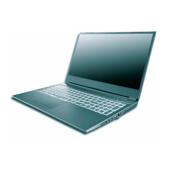
- Page 1 NK50SZ...
- Page 3 Preface Notebook Computer NK50SZ Service Manual...
- Page 4 Preface Notice The company reserves the right to revise this publication or to change its contents without notice. Information contained herein is for reference only and does not constitute a commitment on the part of the manufacturer or any subsequent ven- dor.
- Page 5 This manual is intended for service personnel who have completed sufficient training to undertake the maintenance and inspection of personal computers. It is organized to allow you to look up basic information for servicing and/or upgrading components of the NK50SZ se- ries notebook PC.
- Page 6 Preface IMPORTANT SAFETY INSTRUCTIONS Follow basic safety precautions, including those listed below, to reduce the risk of fire, electric shock and injury to per- sons when using any electrical equipment: 1. Do not use this product near water, for example near a bath tub, wash bowl, kitchen sink or laundry tub, in a wet basement or near a swimming pool.
- Page 7 Preface Instructions for Care and Operation The notebook computer is quite rugged, but it can be damaged. To prevent this, follow these suggestions: Don’t drop it, or expose it to shock. If the computer falls, the case and the components could be damaged. Do not expose the computer Do not place it on an unstable Do not place anything heavy...
- Page 8 Preface 4. Avoid interference. Keep the computer away from high capacity transformers, electric motors, and other strong magnetic fields. These can hinder proper performance and damage your data. 5. Take care when using peripheral devices. Use only approved brands of Unplug the power cord before peripherals.
- Page 9 Preface Battery Precautions • Only use batteries designed for this computer. The wrong battery type may explode, leak or damage the computer. • Do not continue to use a battery that has been dropped, or that appears damaged (e.g. bent or twisted) in any way. Even if the computer continues to work with a damaged battery in place, it may cause circuit damage, which may possibly result in fire.
- Page 10 Preface Related Documents You may also need to consult the following manual for additional information: User’s Manual on CD/DVD This describes the notebook PC’s features and the procedures for operating the computer and its ROM-based setup pro- gram. It also describes the installation and operation of the utility programs provided with the notebook PC. System Startup 1.
-
Page 11: Table Of Contents
Preface Contents Introduction ..........1-1 Top ....................A-3 Bottom ................... A-4 Overview ..................1-1 Main Board ................... A-5 Specifications ..................1-2 LCD ....................A-6 External Locator - Top View with LCD Panel Open ......1-4 HDD ....................A-7 External Locator - Front & Right Side Views .........1-5 Schematic Diagrams......... - Page 12 Preface PCH 8/9 ..................B-26 PCH 9/9 ..................B-27 Audio Codec ................. B-28 KBC-ITE IT5570 ................. B-29 M.2 SSD SATA ................B-30 USB Type-C, M.2 WLAN+BT ............ B-31 USB Type-A, USB Charger ............B-32 RGB KB, Fan, LED, Audio ............B-33 HDD, CCD, TP, LID, PWR SW ..........
-
Page 13: Introduction
Chapter 1: Introduction Overview This manual covers the information you need to service or upgrade the NK50SZ series notebook computer. Information about operating the computer (e.g. getting started, and the Setup utility) is in the User’s Manual. Information about dri- vers (e.g. -
Page 14: Specifications
Introduction Specifications Processor Options Memory Intel® Core™ i7 Processor Dual Channel DDR4 i7-10700 (2.90GHz) Two 260 Pin SO-DIMM Sockets 16MB Smart Cache, 14nm, DDR4-2933MHz, TDP 65W Supporting up to 3200MHz DDR4 Memory Intel® Core™ i5 Processor Memory Expandable up to 32GB Latest Specification Information i5-10600 (3.30GHz) Compatible with 4GB, 8GB or 16GB Modules... - Page 15 Introduction Security M.2 Slots Security (Kensington® Type) Lock Slot Slot 1 for Combo WLAN and Bluetooth Module BIOS Password Slot 2 for PCIe Gen3 x4 SSD Intel® PTT for Systems Without TPM Hardware (Factory Option) Slot 3 for 4G Module (Factory Option) TPM 2.0 Communication Keyboard...
-
Page 16: External Locator - Top View With Lcd Panel Open
Introduction External Locator - Top View with LCD Panel Open Figure 1 Top View 1. PC Camera 2. *PC Camera LED *When the PC camera is in use, the LED will be illuminated. 3. Built-In Microphone 4. Display 5. Power Button 6. -
Page 17: External Locator - Front & Right Side Views
Introduction External Locator - Front & Right Side Views Figure 2 Front View 1. LED Indicators FRONT VIEW Figure 3 Right Side View 1. Multi-in-1 Card Reader RIGHT SIDE VIEW 2. 2-In-1 Audio Jack (Headphones/ Headset) 3. Microphone-In Jack 4. USB 2.0 Port 5. -
Page 18: External Locator - Left Side & Rear View
Introduction External Locator - Left Side & Rear View Figure 4 Left Side View 1. Vent 2. External Display Port 3. HDMI-Out Port LEFT SIDE VIEW 4. USB 3.2 Gen 1 Type-C Port 5. USB 3.2 Gen 1 Type-A Port 6. -
Page 19: External Locator - Bottom View
Introduction External Locator - Bottom View Figure 6 Bottom View 1. Battery 2. Vent 3. Speakers Overheating To prevent your com- puter from overhea- ting, make sure no- thing blocks any vent while the computer is in use. External Locator - Bottom View 1 - 7... -
Page 20: Mainboard Overview - Top (Key Parts)
Introduction Mainboard Overview - Top (Key Parts) Figure 7 Mainboard Top Key Parts 1. KBC-ITE IT5570 1 - 8 Mainboard Overview - Top (Key Parts) -
Page 21: Mainboard Overview - Bottom (Key Parts)
Introduction Mainboard Overview - Bottom (Key Parts) Figure 8 Mainboard Bottom Key Parts 1. CPU (not installed) 2. M.2-Card Connector (LTE Module) 3. Memory Slots DDR4 SO-DIMM 4. PCH 5. M.2-Card Connector (WLAN Module) 6. M.2-Card Connector (SSD Module - PCIE only) 7. -
Page 22: Mainboard Overview - Top (Connectors)
Introduction Mainboard Overview - Top (Connectors) Figure 9 Mainboard Top Connectors 1. Battery Connector 2. External Display Port 3. HDMI-Out Port 4. USB Port 3.2 (Type C) Connector 5. USB Port 3.2 (Type A) Connector 6. USB Port 2.0 (Type A) Connector 7. -
Page 23: Mainboard Overview - Bottom (Connectors)
Introduction Mainboard Overview - Bottom (Connectors) Figure 10 Mainboard Bottom Connectors 1. DC-In Connector 2. Fan Connector 3. J_MUX Connector 4. Speaker Connector 5. LCD Connector Mainboard Overview - Bottom (Connectors) 1 - 11... - Page 24 Introduction 1 - 12...
-
Page 25: Disassembly
Chapter 2: Disassembly Overview This chapter provides step-by-step instructions for disassembling the NK50SZ series notebook’s parts and subsystems. When it comes to reassembly, reverse the procedures (unless otherwise indicated). We suggest you completely review any procedure before you take the computer apart. -
Page 26: Maintenance Tools
Disassembly NOTE: All disassembly procedures assume that the system is turned OFF, and disconnected from any power supply (the battery is removed too). Maintenance Tools The following tools are recommended when working on the notebook PC: • M3 Philips-head screwdriver •... -
Page 27: Maintenance Precautions
Disassembly Maintenance Precautions The following precautions are a reminder. To avoid personal injury or damage to the computer while performing a removal and/or replacement job, take the following precautions: Power Safety Don't drop it. Perform your repairs and/or upgrades on a stable surface. If the computer falls, the case and other components Warning could be damaged. -
Page 28: Disassembly Steps
Disassembly Disassembly Steps The following table lists the disassembly steps, and on which page to find the related information. PLEASE PERFORM THE DISASSEMBLY STEPS IN THE ORDER INDICATED. To remove the Battery: To remove the Wireless LAN Module: 1. Remove the battery page 2 - 5 1. -
Page 29: Removing The Battery
Disassembly Removing the Battery Figure 1 Battery Removal 1. Turn the computer off, and turn it over. 2. Slide the latch in the direction of the arrow (Figure 1a). a. Slide the latch in the 3. Slide the latch in the direction of the arrow. direction of the arrow. -
Page 30: Removing The Hard Disk Drive
Disassembly Removing the Hard Disk Drive Figure 2 The hard disk drive can be taken out to accommodate other 2.5" serial (SATA) hard disk drives with a height of 7mm HDD Assembly (h). Follow your operating system’s installation instructions, and install all necessary drivers and utilities (as outlined in Removal Chapter 4 of the User’s Manual) when setting up a new hard disk. - Page 31 Disassembly 5. Remove screws from the HDD assembly (Figure 3d). Figure 3 6. Slightly lift and pull the hard disk assembly in the direction of arrow (Figure 3e HDD Assembly 7. Lift the hard disk assembly out of the bay (Figure 3f Removal (cont’d.) 8.
-
Page 32: Removing The Keyboard
Disassembly Removing the Keyboard Figure 4 1. Turn off the computer, remove the battery (page 2 - 5) and bottom cover (page 2 - Keyboard Removal 2. Remove screws from the bottom of the computer. 3. Open it up with the LCD on a flat surface before pressing at point to release the keyboard module (use the spe- a. -
Page 33: Removing And Installing The Processor
Disassembly Removing and Installing the Processor Figure 5 Processor Processor Removal Procedure Removal 1. Turn off the computer, remove the battery (page 2 - 5) and bottom cover (page 2 - Procedure 2. Disconnect the cable and remove screws from the CPU fan & heat sink unit in the order indicated on the label (i.e screw first through to screw... - Page 34 Disassembly 4. Press down and hold the latch (with the latch held down you will be able to release it). 5. Move the latch and bracket fully in the direction indicated to unlock the CPU(Figure 6d). Figure 6 6. Carefully (it may be hot) lift the CPU up out of the socket (Figure 6e).
- Page 35 Disassembly Processor Installation Procedure Figure 7 1. Insert the CPU ; pay careful attention to the pin alignment (Figure 7a), it will fit only one way (DO NOT FORCE Processor Installation IT!). 2. Move the bracket and latch fully in the direction indicated to lock the CPU. 3.
-
Page 36: Removing The System Memory (Ram)
Disassembly Removing the System Memory (RAM) Figure 8 RAM Module The computer has two memory sockets for 260 pin Small Outline Dual In-line Memory Modules (SO-DIMM) supporting Removal DDR4 3200 MHz. The main memory can be expanded up to 16GB. The total memory size is automatically detected by the POST routine once you turn on your computer. -
Page 37: Removing The M.2 Ssd Module
Disassembly Removing the M.2 SSD Module Figure 9 M.2 SSD Module 1. Turn off the computer, remove the battery (page 2 - 5) and bottom cover (page 2 - Removal 2. The M.2 SSD module will be visible at point on the mainboard (Figure 9a). -
Page 38: Removing The Wireless Lan Module
Disassembly Removing the Wireless LAN Module Figure 10 Wireless LAN 1. Turn off the computer, remove the battery (page 2 - 5) and bottom cover (page 2 - Module Removal 2. The Wireless LAN module will be visible at point on the mainboard (Figure 10a). -
Page 39: Wireless Lan, Combo, & Lte Module Cables
Disassembly Wireless LAN, Combo, & LTE Module Cables Note that the cables for connecting to the antennae on WLAN, WLAN & Bluetooth Combo, and LTE modules are not labelled. The cables/covers (each cable will have either a black or transparent cable cover) are color coded for identifi- cation as outlined in the table below. -
Page 40: Removing The Lte Module
Disassembly Removing the LTE Module Figure 11 LTE Module 1. Turn off the computer, remove the battery (page 2 - 5) and bottom cover (page 2 - Removal 2. The LTE module will be visible at point on the mainboard (Figure 11a). -
Page 41: Removing The Ccd
Disassembly Removing the CCD Figure 12 CCD Removal 1. Turn off the computer, turn it over to remove the battery (page 2 - 2. Lay the computer down on a flat surface with the top case up forming a 90 degree angle. Carefully remove the a. - Page 42 Disassembly 5. Disconnect the cable (Figure 13c). Figure 13 6. Remove the CCD module (Figure 13d). CCD Removal 7. Reverse the process to install a new CCD module. (cont’d) c. Disconnect the cable. d. Remove the CCD mod- ule. 11.
-
Page 43: Part Lists
Appendix A:Part Lists This appendix breaks down the NK50SZ series notebook’s construction into a series of illustrations. The component part numbers are indicated in the tables opposite the drawings. Note: This section indicates the manufacturer’s part numbers. Your organization may use a different system, so be sure to cross-check any relevant documentation. -
Page 44: Part List Illustration Location
Part List Illustration Location The following table indicates where to find the appropriate part list illustration. Table A - 1 Part List Illustration Part Location page A - 3 page A - 4 Bottom page A - 5 Main Board page A - 6 page A - 7 A - 2... -
Page 45: Top
Figure A - 1 Top A - 3... -
Page 46: Bottom
Bottom Figure A - 2 Bottom A - 4 Bottom... -
Page 47: Main Board
Main Board Figure A - 3 Main Board Main Board A - 5... -
Page 48: Lcd
Figure A - 4 A - 6 LCD... -
Page 49: Hdd
Figure A - 5 HDD A - 7... - Page 50 A - 8...
-
Page 51: Schematic Diagrams
Schematic Diagrams Appendix B: Schematic Diagrams This appendix has circuit diagrams of the NK50SZ notebook’s PCB’s. The following table indicates where to find the appropriate schematic diagram. Diagram - Page Diagram - Page Diagram - Page Table B - 1... -
Page 52: System Block Diagram
Schematic Diagrams System Block Diagram NK50S5 System Block Diagram (Comet Lake S) VDD3,VDD5 SHEET 36 nVIDIA 5V,5VS,3VA,3.3V,3.3VS,VCCST PEG*4 Nvidia GEN2 Comet Lake S SHEET 35 N17S-G5/GDDR5 SO-DIMM 1 SHEET 7 SHEET 9,10,11,12, 2.5V,VDDQ,VTT_MEM 13,14 DDR4 Channel A SHEET 38 SHEET 8 SO-DIMM 2 LGA1200 Socket DDR4 Channel B... -
Page 53: Processor 1/5
Schematic Diagrams Processor 1/5 U30B U30A Zo=50ohm, L<4.6" Zo=50ohm, L<4.6" DDR4 (IL)/DDR4 (NIL) DDR4 (IL)/DDR4 (NIL) M_A_DQ[63:0] M_B_DQ[63:0] M_A_DQ60 AY18 M_B_DQ61 AU20 DDR0_DQ_63/DDR1_DQ_47 DDR0_CKP_3 DDR1_DQ_63/DDR1_DQ_63 DDR1_CKP_3 M_A_DQ59 AW18 M_B_DQ58 AV20 DDR0_DQ_62/DDR1_DQ_46 DDR0_CKN_3 DDR1_DQ_62/DDR1_DQ_62 DDR1_CKN_3 M_A_DQ56 M_B_DQ57 AT19 AT21 DDR0_DQ_61/DDR1_DQ_45 DDR0_CKP_2 DIFF=88ohm, L<4.6"... -
Page 54: Processor 2/5
Schematic Diagrams Processor 2/5 85 ohm Space: 15mil Length: 3000~8000mil To GPU 85 ohm Via: 4 U30C Space: 15mil PEG TX AC CAPTURE NEAR FORM GPU Length: 3000~8000mil CPU 0.22U_10V_X5R_04 Via: 4 PCIE_PEG_RXP15 PCIE_PEG_TXP15 PCIE_PEG_RXN15 PCIE_PEG_TXN15 PCIE_PEG_RXP14 PCIE_PEG_TXP14 PCIE_PEG_RXN14 PCIE_PEG_TXN14 PCIE_PEG_RXP13 PCIE_PEG_TXP13 BOT NEAR TO CPU... -
Page 55: Processor 3/5
Schematic Diagrams Processor 3/5 CFG TABLE Stall reset sequence after PCU PLL lock until de-asserted: CFG[0] 1 = (Default) Normal Operation; No stall. 0 = Stall. CFG[1] Reserved configuration lane. PCI Express* Static x16 Lane Numbering Reversal. CFG[2] 1 = Normal operation 0 = Lane numbers reversed. -
Page 56: Processor 4/5
Schematic Diagrams Processor 4/5 U30F U30G U30H U30I U30J VCORE VCORE VCORE VCORE AK31 AP11 VSS_247 VSS_312 VSS_117 VSS_182 VSS_1 VSS_66 AK33 AP13 210A 210A VSS_248 VSS_313 VSS_118 VSS_183 VSS_2 VSS_67 AK35 AV10 VSS_249 VSS_314 VSS_119 VSS_184 VSS_3 VSS_68 AK37 AP27 AV12 VSS_250... -
Page 57: Processor 5/5
VCCIO_0_9 VCCGT_36 CML S 610244 Ver0.8 CML S 610244 Ver0.8 VCCIO_0_10 VCCGT_37 Processor 5/5 1X22U 1X1U VCCIO_0_11 VCCGT_38 *H8_0D5_0 *H8_0D5_0 1X1U CLEVO CFL S VCCGT_39 VCCST VCCSTG VCCSA_SENSE CLEVO CFL S VCCSA_SENSE VCCGT_40 41,42 VSS_SA_IO_SENSE 1X22U VSSSA_SENSE VCCGT_41 1X1U VCCGT_42... -
Page 58: Ddr4 Cha So-Dimm_0
Schematic Diagrams DDR4 CHA SO-DIMM_0 STD TYPE Channel A SO-DIMM 0[RAM1] VDDQ VTT_MEM H=8.0mm J_DIMMA_1B 2.5V J_DIMMA_1A M_A_DQ[63:0] VDD19 VDD18 M_A_DQ0 M_A_CLK_DDR0 CK0_T VDD17 M_A_DQ1 M_A_CLK_DDR#0 CK0_C VDD16 VPP2 M_A_DQ2 M_A_CLK_DDR1 CK1_T VDD15 VPP1 M_A_DQ3 M_A_CLK_DDR#1 CK1_C VDD14 M_A_DQ4 VDD13 3.3VS M_A_DQ5 M_A_CKE0... -
Page 59: Ddr4 Chb So-Dimm_0
Schematic Diagrams DDR4 CHB SO-DIMM_0 VTT_MEM Channel B SO-DIMM 0[RAM2] VDDQ J_DIMMB_1B STD TYPE H=4.0mm VDD19 2.5V VDD18 VDD17 J_DIMMB_1A M_B_DQ[63:0] VDD16 VPP2 VDD15 VPP1 M_B_DQ0 M_B_CLK_DDR0 CK0_T VDD14 M_B_DQ1 3.3VS M_B_CLK_DDR#0 CK0_C VDD13 M_B_DQ2 M_B_CLK_DDR1 CK1_T VDD12 M_B_DQ3 M_B_CLK_DDR#1 CK1_C VDD11 M_B_DQ4... -
Page 60: Vga Pci-E Interface
Schematic Diagrams VGA PCI-E Interface NH70EG NO STUFF U28A COMMON 2020 1/17 N18S ADD 1/14 PCI_EXPRESS NEAR GPU PEX_VDD GP107S TU117S UNDER GPU TU117S GP107S PEX_CVDD AA22 AA14 PEX_DVDD PEX_WAKE C637 C639 C640 C641 C429 C638 AB23 PEX_RST PEX_DVDD DGPU_PEX_RST# *1u_6.3V_X5R_04 *1u_6.3V_X5R_04 *4.7u_6.3V_X6S_06... -
Page 61: Vga Frame Buffer Interface
Schematic Diagrams VGA Frame Buffer Interface Term Description The total trace length measured NH70EG NO STUFF from GPU ball to capacitor is Under GPU Frame Buffer Interface no more than 150 mil U28E The total trace length measured from GPU ball to capacitor is no Near GPU more than 850 mil COMMON... -
Page 62: Vga Frame Buffer A
Schematic Diagrams VGA Frame Buffer A U26B U26C INS36742371 INS36742055 BGA170 BGA170 COMMON 10,12 FBA_CMD[31:0] COMMON Normal FBA_CMD12 FBA_CMD15 FBA_SOE0 MF_VSS/SOE* FBA_CLK0 FBA_CMD5 FBVDDQ FBA_CMD0 add 1k to VSS FBA_CLK0# FBA_D[31:0] FBA_CMD8 U26D U26A FBA_CMD10 A0_A10 INS36741160 INS36741501 FBA_CMD11 BGA170 BGA170 A1_A9 FBA_CMD2... - Page 63 Schematic Diagrams VGA Frame Buffer A U25B U25C INS36744718 INS36744402 BGA170_MIRR BGA170_MIRR R299 0_04 COMMON COMMON 10,11 FBA_CMD[31:0] FBVDDQ Mirrored FBA_CMD28 FBA_CLK1 FBA_CMD31 FBA_SOE3 FBA_CLK1# SOE*/MF_VDD FBA_CMD21 add 1k to VDD FBA_CMD16 FBA_D[63:32] FBVDDQ FBA_CMD24 U25D U25A INS36744800 INS36744320 FBA_CMD26 BGA170_MIRR BGA170_MIRR A0_A10...
-
Page 64: Vga I/O
2.2u_6.3V_X5R_04 2.2u_6.3V_X5R_04 2.21K_1%_04 VGA_GPIO16 *10K_04 GPU_N18S GPU_N18S GPU_N18S VGA_GPIO23 *10K_04 VOUT VBIAS 3.3VS GPIO18_FP_FUSE C635 FA7609A6 0.1u_6.3V_X5R_02 CLEVO CO. dGPU_PWR_EN 14,44 NVVDD 10K_04 R552 GPU_N18S GPU_N18S VGA_GPIO1 7,8,15,16,18,21,22,23,24,25,27,28,29,30,33,34,35,37,39,41,42,44,45,46,54 3.3VS 10K_04 Title Title Title [13] VGA I/O [13] VGA I/O [13] VGA I/O... -
Page 65: Vga Nvvdd Coupling
Schematic Diagrams VGA NVVDD Coupling NVVDD under U28C U28I U28H NVVDD C105 C165 COMMON COMMON COMMON 1u_6.3V_X5R_04 1u_6.3V_X5R_04 1u_6.3V_X5R_04 *1u_6.3V_X6S_04 11/14 VDD 1 of 2 6/14 XVDD NVVDD NVVDD 13/14 GND XVDD XVDD AB17 XVDD XVDD AB20 XVDD XVDD AB24 C115 C119 C110... -
Page 66: Crt
Schematic Diagrams J_CRT1 5VS_CRT DS15146BAC067 6-19-31001-003 6-20-14X60-015 RB751S-40H DAC_RED DS1514XXXC067-1 FCM1005MF-600T01 FRED DAC_GREEN FCM1005MF-600T01 FGRN Footprint TBC 6-06-75140-068 R343 R327 DAC_BLUE FCM1005MF-600T01 FBLUE 2.2K_04 2.2K_04 C183 C162 C144 C182 C161 C143 VGA_SDA 6-13-36R01-28C VGA_HSYNC VGA_HS_R R338 36_1%_04 VGA_VSYNC R333 36_1%_04 VGA_VS_R VGA_SCL C476... -
Page 67: Hdmi
Schematic Diagrams HDMI J_HDMI1 16-A1970-1A03-0 HDMI_5VS PN = 6-21-14240-019 PCB Footprint = c-16-a197x VOUT C521 C526 C527 HDMI_HPD-C-R *10u_6.3V_X5R_06 22u_6.3V_X5R_06 22u_6.3V_X5R_06 HOT PLUG DETECT AP2331W -7 DDC/CEC GND PN = 6-02-23317-970 HDMI_SDA-C-R HDMI_SCL-C-R PCB Footprint = m-sot23-123 RESERVED TMDS_CLOCK#J TMDS CLOCK- R434 470_04 R450... -
Page 68: Edp Panel Conn
Schematic Diagrams EDP Panel Conn. PANEL CONNECTOR PANEL POWER VLED OPEN_2A SHORT C437 0.1u_10V_X5R_04 CPU_EDP_TXN0_C J_LCD1 CPU_EDP_TXN0 C436 0.1u_10V_X5R_04 CPU_EDP_TXP0_C lvdfh-03008-tp00+ CPU_EDP_TXP0 PLVDD PN = 6-21-44K00-030 C489 C487 C485 CPU_EDP_TXN1_C C435 0.1u_10V_X5R_04 PCB Footprint = lvdfh-030xx-tx00 80 mil *0.22u_25V_X7R_06 CPU_EDP_TXN1 C434 0.1u_10V_X5R_04 CPU_EDP_TXP1_C... -
Page 69: Pch 1/9
Schematic Diagrams PCH 1/9 U43A LAN_W UP# BF15 BD24 PLT_RST# GPP_A11/PME# GPP_B13/PLTRST# AH16 RSVD_18 GPP_G16/GSXCLK AH14 AC39 RSVD_19 GPP_G12/GSXDOUT AG17 RSVD_20 GPP_G13/GSXSLOAD AF17 GSXDIN GPP_G_14_GSXDIN: RSVD_21 GPP_G14/GSXDIN DMI AC COUPLING FULL VOLTAGE MODE SPI = 1"~6.5" GPP_G15/GSXSRESET# WHEN SAMPLED LOW AU19 Zo=50ohm AP17... - Page 70 Schematic Diagrams PCH 2/9 U43B Zdiff=85 ,Length=3" ~ 12" CPU_DMI_TXN0 DMI_RXN0 USB2N_1 USB_PN1 Type-A USB2.0 PORT1(Audio/B) CPU_DMI_TXP0 USB_PP1 DMI_RXP0 USB2P_1 PCH_DMI_RXN0 DMI_TXN0 USB2N_2 USB_PN2 Type-A USB3.1 PORT2(M/B) PCH_DMI_RXP0 DMI_TXP0 USB2P_2 USB_PP2 CPU_DMI_TXN1 DMI_RXN1 USB2N_3 USB_PN3 AH10 4G LTE PORT3(M/B) CPU_DMI_TXP1 USB_PP3 DMI_RXP1 USB2P_3...
-
Page 71: Pch 3/9
Schematic Diagrams PCH 3/9 SATA_LED# R489 10K_04 3.3VS U43C SCI#_R R526 10K_04 GPIO2_FB_TGL_REQ_PCH R518 10K_04 CL_CLK PCIE9_RXN/SATA0A_RXN SMI#_R R565 10K_04 CL_DATA PCIE9_RXP/SATA0A_RXP 2020 1/22 Modify SATAGP3 R482 10K_04 CL_RST# PCIE9_TXN/SATA0A_TXN PCIE9_TXP/SATA0A_TXP W /_SSD SATA SATA_PW R_EN GPP_G8 SSD0_PW R_DN# GPP_G9 PCIE10_RXN/SATA1A_RXN AC35 GPP_G10... - Page 72 Schematic Diagrams PCH 4/9 R376 R377 VDD3 U43D 0_04 *45.3K_1%_04 CLOSE TO PCH Zo=50ohm <14" RTC3.2V R135 47_04 PCH_HDA_BCLK BD15 ISH_GP_6_R HDA_BITCLK HDA_BCLK GPP_A12/BMBUSY#/ISH_GP6/SX_EXIT_HOLDOFF# PCH_HDA_RST# R462 47_04 BA15 HDA_RST# HDA_RST# GPP_A8/CLKRUN# ECCLKRUN# HDA_SDIN0 HDA_SDI0 LAN_DISABLE_N BC11 HDA_SDI1 GPD11/LANPHYPC 2020 2/5 VCC_RTC Follow EC COMMON Name R132...
-
Page 73: Pch 5/9
Schematic Diagrams PCH 5/9 TEST SETUP MENU TABLE BOARD STYLE DISABLED (DEFAULT) TEST SETUP MENU ENABLED U43E DESIGN NOTE: TEST SETUP MENU JUMPER HDMI_HPD CPU_C10_GATE_M 2020 2/13 ADD GPP_I0/DDPB_HPD0 GPP_I7/DDPC_CTRLCLK GPP_I8 VGA_HPD GPP_I1/DDPC_HPD1 GPP_I8/DDPC_CTRLDATA 3.3VS GPP_I2/DDPD_HPD2 GPP_I5/DDPB_CTRLCLK HDMI_CTRLCLK GPP_I3/DDPE_HPD3 GPP_I6/DDPB_CTRLDATA HDMI_CTRLDATA 3.3VS R530... - Page 74 Schematic Diagrams PCH 6/9 U43G BC17 GPP_A16/CLKOUT_48 PCH_XDP_CLK_DN CPU_24MHZ_R_DP CLKOUT_CPUNSSC_P CLKOUT_ITPXDP PCH_XDP_CLK_DP CPU_24MHZ_R_DN CLKOUT_CPUNSSC CLKOUT_ITPXDP_P Zdiff=85 ,Length=4" ~ 9" CLKOUT_CPUPCIBCLK PCH_CPU_PCIBCLK_R_DN Zdiff=85 ,Length=4" ~ 9 " PCH_CPU_BCLK_R_DP CLKOUT_CPUBCLK_P CLKOUT_CPUPCIBCLK_P PCH_CPU_PCIBCLK_R_DP PCH_CPU_BCLK_R_DN CLKOUT_CPUBCLK VGA_PEXCLK# CLKOUT_PCIE_N0 VGA_PEXCLK CLKOUT_PCIE_P0 XTAL24_OUT_PCH Zo=50 ,Length<1000mil XTAL24_OUT XTAL24_IN_PCH XTAL24_IN CLKOUT_PCIE_N1...
-
Page 75: Pch 7/9
Schematic Diagrams PCH 7/9 U43H 1.0VA C238 0.1u_10V_X5R_04 AA23 AM22 1.0VA VCCPRIM_1P0_4 VCCPRIM_1P0_3 AA25 R144 3.3VA *20mil_short_04 VCCPRIM_1P0_5 VDD3 AB23 BC24 C261 VCCPRIM_1P0_6 VCCPDSW_3P3 C250 C262 *0.1u_10V_X5R_04 AB26 C225 CLOSE TO PCH VCCPRIM_1P0_7 0.1u_10V_X5R_04 *0.1u_10V_X5R_04 *0.1u_10V_X5R_04 AB28 BC31 (1-3 mm) VCCPRIM_1P0_8 VCCPGPPA AD23... - Page 76 Schematic Diagrams PCH 8/9 U43L BG14 U43I VSS_333 VSS_213 VSS_215 VSS_306 VSS_217 VSS_307 VSS_1 VSS_299 VSS_219 VSS_308 BD21 VSS_221 VSS_309 VSS_214 VSS_300 BD25 BG44 VSS_223 VSS_310 VSS_216 VSS_301 BF44 M/B SIDE VSS_218 VSS_302 VSS_225 VSS_311 BF45 VSS_220 VSS_303 VSS_227 VSS_312 H5_5D3_7 VSS_229 VSS_313...
-
Page 77: Pch 8/9
Schematic Diagrams PCH 9/9 U43J Hardware Straps (5) AU22 RSVD_17 RSVD_11 RSVD_16 RSVD_15 GPP_B18 / GSPI0_MOSI RSVD_14 No Reboot Internal PD 20K CMOS RSVD_13 0 = Disable “No Reboot” mode. (Default) 1 = Enable “No Reboot” mode. RSVD_12 VSS_2 R407 *4.7K_04 VSS_29 RSVD_10... -
Page 78: Audio Codec
Schematic Diagrams Audio Codec ALC293D HEADPHONE_L HEADPHONE_R SHORT 3.3V V1.5 1.5VS MIC1_VREFO_L 30mils VOUT SLEEVE SLEEVE Layout trace > 40 mil suggest to implement shapes. C519 R380 C522 1u_6.3V_X5R_04 47K_1%_04 1u_6.3V_X5R_04 R485 0_04 E >K' SHDN# AUDG /'/d > AUDG 5VS_AUD C518 NCT3705U-A... -
Page 79: Kbc-Ite It5570
Schematic Diagrams KBC-ITE IT5570 VDD3 IT5570 BAV99: 6-06-00993-011 MODEL_ID PROJECT NAME 29,39,43 SMC_BAT NK50 BAV99CL VDD3 C622 C381 C342 C391 NK50_UMA 29,39,43 SMD_BAT BAV99CL 10u_6.3V_X5R_06 0.1u_6.3V_X5R_02 0.1u_6.3V_X5R_02 0.1u_6.3V_X5R_02 KBC_AVDD NK50S5_BOARD_ID HCB1005KF-121T20 MODEL_ID R210 10K_04 29,43 BAT_DET VDD3 C388 VDD3 BAV99CL NK50SZ_UMA_BOARD_ID 0.1u_6.3V_X5R_02 C343... -
Page 80: M.2 Ssd Sata
Schematic Diagrams M.2 SSD SATA NGFF_M (M2) SSD (PCIe Gen2 x4/SATA) 3.3VS J_SSD1 NFSM0-S6701-TP40 120mil P/N = 6-21-84K70-075 SSD1_3.3VS PCB Footprint = NXSM0-S67XX-XX85 R535 C285 C286 C284 GND13 *10K_04 0.1u_6.3V_X5R_02 0.1u_6.3V_X5R_02 22u_6.3V_X5R_06 GND12 3.3V8 GND11 3.3V7 PEDET(NC-PCIe/GND-SATA) 3.3V6 CLOSE TO PINS 70,72,74 NC18 SUSCLK(32Khz)(O) CO-LAY... -
Page 81: Usb Type-C, M.2 Wlan+Bt
Schematic Diagrams USB Type-C, M.2 WLAN+BT TYPE-C USB3.1 GEN 2 PORT (PORT2,3) USBVCC3.1_1 100mil 100mil J_TYPEC1 close to connector R531 220K_1%_04 UCF3T-21S01-0P21 R533 220K_1%_04 PN = 6-21-B4K50-024 C273 C279 PCB Footprint = ucf3t-21xxx-xxx1 10u_6.3V_X5R_06 A_URXP_SW 2_J C587 0.33u_6.3V_X5R_02 USB3_RXP2 0.1u_6.3V_X5R_02 C588 0.33u_6.3V_X5R_02 A_URXN_SW 2_J... -
Page 82: Usb Type-A, Usb Charger
Schematic Diagrams USB Type-A, USB Charger VDD5 TYPE-A USB2.0 PORT (PORT5) USBVCC_CH 80mil 80mil VOUT C351 C357 10u_6.3V_X5R_06 0.1u_6.3V_X5R_02 uP7549UMA5-20 USB CHARGER (Optional) C369 22u_6.3V_X5R_06 Default Low USB_DD_ON# 29,35,36,45 DD_ON PRE# C368 22u_6.3V_X5R_06 60 mil USB_PN5_CHG USB_PN5 USBVCC_CH R249 USB_PP5_CHG 100K_1%_04 C356 0.1u_6.3V_X5R_02... -
Page 83: Rgb Kb, Fan, Led, Audio
Schematic Diagrams RGB KB, Fan, LED, Audio J_KB1 FOR NB50 RGB KB LED FP226H-026S10M FOR 15" K/B <FUNCTION> AUDIO/B KB-SI0 VDD3 KB-SI0 KB-SI1 KB-SI1 KB-SI2 RGBKB_PW R KB-SI2 KB-SI3 J_MUX1 J_RGBKB1 KB-SI3 KB-SI4 FP201H-040S10M C251 4.7u_6.3V_X5R_04 R172 KB-SI4 KB-SI5 PN = 6-20-94K20-140 KB-SI5 KB-SI6 *100K_1%_04... -
Page 84: Hdd, Ccd, Tp, Lid, Pwr Sw
Schematic Diagrams HDD, CCD, TP, LID, PWR SW TOUCH PAD HDD CONNECT TP_VCC 3.3VS R157 *20mil_short_04 J_HDD1 Gen2 JHDD_SATA_TXP2 C626 0.01u_16V_X7R_04 C209 1u_6.3V_X5R_02 SATA_TXP2 21 J_TP2 C233 0.1u_6.3V_X5R_02 JHDD_SATA_TXN2 C625 0.01u_16V_X7R_04 SATA_TXN2 21 TP_CLK_J JHDD_SATA_RXN2 C624 0.01u_16V_X7R_04 SATA_RXN2 TP_DATA_J JHDD_SATA_RXP2 C623 0.01u_16V_X7R_04 SATA_RXP2... -
Page 85: 5V, 5Vs, 3.3Va, 3.3V, 3Vs
Schematic Diagrams 5V, 5VS, 3.3VA, 3.3V, 3VS 1.0VA VDD3 NOTE: VDD3 C318 G5016 C613 1.0V_VCCST Ton need <10ms VCCST G5016 TURN-ON TIME=1.21ms 0.1u_10V_X7R_04 0.1u_6.3V_X5R_02 TC7SZ08FU 3.3VA SUSBC_EC# 1.0V SUSC# 35,38 1V_VCCST SUSC#_PCH VCCST 3.3VA OUT2 OUT1 22,29 SUSC#_PCH OUT2 OUT1 C344 SHORT R223... -
Page 86: Vdd3, Vdd5
Schematic Diagrams VDD3, VDD5 O.C.P 10.6A~13A PR266 PR267 18K_1%_04 18K_1%_04 EN_3V EN_5V PC281 PJ16 *CV-40mil 1000p_50V_X7R_04 2020 2/17 POWER PU22 VREG3 2.5A PC266 PC268 PC267 PC272 PC273 PC274 PC259 PC152 VDD3 PC271 1u_6.3V_X5R_04 VREG3 PGOOD PC275 PC276 VDD5 PR269 0_06 PR271 0_06 VBST2... -
Page 87: A, Vccst/Stg/Sfr
Schematic Diagrams 1.05A, VCCST/STG/SFR VDD3 PC231 PC236 PC232 PR251 PU21 *47K_04 1.0VA SY8288RAC VDD_1.0A_PW RGD VDD_1.0A_BST VDD_1.0A_BST_R PL18 1.0VA BCIHP-0735-0R68M-NL V1.0 PJ41 VTT_SELECT VTT VR Output Voltages PR249 PC235 PCB Footprint = BCIHP0735A 1.1 V VDD_1.0A_SW 0_06 0.1u_10V_X7R_04 high (V1.1S_VTT) 1.05 V PR256 PJ40... -
Page 88: B - 38 Vddq, Vtt_Mem, 2.5V
Schematic Diagrams VDDQ, VTT_MEM, 2.5V O.C.P 14A~17.4A PC263 PC261 PC262 RB0540S2 G5616BRZ1U PC37 PC36 VDDQ_R VTT_MEM(0.6V) 0.1u_10V_X7R_04 VDDQ(1.2V) 10u_6.3V_X5R_06 VDDQ_VBST VLDOIN VBST PJ43 EMR1 VTT_MEM_R VDDQ_DRVH VTT_MEM DRVH PQ20 PL21 VDDQ_R PJ42 0_06 PC41 PR72 AON6992 TMPC0603H-1R0M-Z01 SHORT VDDQ_L VTTGND VDDQ 22u_6.3V_X5R_06 *28mil_short_06... -
Page 89: Mp2979
Schematic Diagrams MP2979 VDD3 VRACPU_PWM1 VRACPU_PWM1 VR_VDD18 VDD3 VR_EN VRACPU_PWM2 100K_1%_04 3.3V VRACPU_PWM2 *CV-40mil *0.1u_16V_X7R_04 VRACPU_PWM3 VRACPU_PWM3 18,27,29 ALL_SYS_PWRGD PJ17 *OPEN-1mm OPEN-1mm PR111 *0_04 VRAGT_PWM1 VRAGT_PWM1 SHORT VRACPU_PE EC_MP2988_EN RB751S-40H 3.3V VRA_STB PR10 VRA_STB 40,41 100K_1%_04 *0.1u_16V_X7R_04 VCCST VRACPU_CS1 VRACPU_CS1 VRACPU_CS2 VRACPU_CS2 VRACPU_CS3... -
Page 90: B - 40 Vcore
Schematic Diagrams VCore VCORE OUTPUT STAGE 2020 2/6 Power Modify 5.5A Co-lay Phase 1 PC120 3.3V PC156 PC121 PC282 PC125 PC130 PU13 *MP86941GQVT-Z PC117 VIN1 PC140 VIN2 *1u_6.3V_X6S_04 BST_PWM1 AGND VCORE VCORE PR156 *0_04 PC149 39,40 VRACPU_PWM1 *1u_25V_X7R_06 PL12 PR159 *0_04 SW_PWM1 PC128... -
Page 91: Vccgt, Vccsa
Schematic Diagrams VCCGT, VCCSA VccGT OUTPUT STAGE 2020 2/6 Power Modify Co-lay 5.5A 3.3V PC194 PC196 PC288 PC197 PC198 PU17 MP86903-CGLT-Z PC199 VIN1 PC193 VIN2 1u_6.3V_X6S_04 GT_BST1 AGND VCCGT PR196 0_04 PC192 39,41 VRAGT_PWM1 PL15 PC191 PC223 PC190 1u_25V_X7R_06 GT_SW1 PR195 0_04 39,40,41... -
Page 92: Vccio
Schematic Diagrams VCCIO PJ28 PR158 VDD3 OPEN 3.3_06 *CV-40mil PR172 100K_04 3.3VA O.C.P 7.6A PR164 0_04 VCCIO PR173 *0_04 22,37 CPU_C10_GATE PJ29 PC142 0.22u_16V_X7R_06 PU14 VCCIO SHORT SHORT PL10 1/15 PC147 PC146 PC134 BCIHP-0735-0R68M-NL PJ32 GPU VCCIO = 0.975V VCCIO_R UMA VCCIO = 0.95V PCB Footprint = BCIHP0735A PC166... -
Page 93: Ac_In, Charger
Schematic Diagrams AC_In, Charger SMART CHARGER TI24780S 2020 1/15 POWER Bryan modify J_DC_CON1 MDL914S2 MDL914S2 VDD3 Charge current Limit 3.42A PC155 0.1u_25V_X7R_06 287K_1%_04 EML1 50287-00601-V01 PQ13 PQ12 HCB2012KF-800T80 P/N = 6-20-43210-106 MDU1512 MDU1721 ILIM PCB Footprint = 50287-006-r ULTRASO-8 ULTRASO-8 EML2 PRS2 75K_1%_04... -
Page 94: Nvvdd
Schematic Diagrams NVVDD NVVDD PHASE 1 ~2 NVVDD FOR N17_VGA D02 2018/1/10 1.8V Add R2319 for isolate power *0_04 R322 PJ35 *CV-40mil PR229 10K_04 NVVDD PHASE 1 ~2 3.3V PR212 1666_DGPU_ON *0_04 *0.1u_10V_X7R_04 PC213 PR228 0_04 NV_NVVDD_EN 20170728 PR213 0_04 GPU_PWR_VID NVVDD FOR N17_VGA PR211... -
Page 95: Pex_Vdd, 1.8V
C195 C189 *0.22u_10V_X5R_04 1u_6.3V_X5R_02 *0.047u_10V_X7R_04 3.3VA 4,19,21,22,25,27,35,37,42,54 VDD_AON 9,13,44,46 VDD_RUN 9,10,13 VDD3 13,18,19,22,25,27,28,29,30,31,33,34,35,36,37,39,41,42,43,44,45,46 1.8V PEX_VDD VDD3 13,18,19,22,25,27,28,29,30,31,33,34,35,36,37,39,41,42,43,44,45,46 31,32,33,35,38,41,44,46 CLEVO CO. 3.3VS 7,8,13,15,16,18,21,22,23,24,25,27,28,29,30,33,34,35,37,39,41,42,44,46,54 3.3V 3,13,18,28,30,31,34,35,38,39,40,41,42,44,46,47 Title Title Title [45]PEX_VDD/1.8V [45]PEX_VDD/1.8V [45]PEX_VDD/1.8V Size Size Size Document Number Document Number Document Number Custom... -
Page 96: Fbvddq
Schematic Diagrams FBVDDQ FBVDDQ FOR N17 VGA NB50TZ NO STUFF 3.3V FBVDDQ PR55 10K_04 PR56 820K_1%_06 *CV-1mm PC29 PC186 PC184 PC185 OPEN-1mm PR51 PC27 SHORT 0_06 0.1u_10V_X5R_04 PR54 30K_1%_04 EN_PSV NV_FBVDDQ_EN 1.35VS O.C.P 40A~50A PR52 0_06 PL13 PR197 TMPC0603H-1R0M-Z01 FBVDDQ 2.2_04 VOUT PCB Footprint = BCIHP0735A... -
Page 97: M.2 3G/Lte
Schematic Diagrams M.2 3G/LTE CURRENT 2A ,DON'T DROP BELOW 3.135V 3G_3.3V 3G CARD 3G_3.3V 80 mils J_3G1 3GLTE 3GLTE C563 220u_6.3V_6.3*4.4 M2_SIM_DET R441 C562 0.1u_6.3V_X5R_02 3GLTE CONFIG_2 3.3V4 100K_04 GND10 3.3V3 3GLTE C564 0.1u_6.3V_X5R_02 3GLTE GND9 3.3V2 CONFIG_1 SUSCLK(32Khz)(O) SIM_DET M2_SIM_DET Reset#(O)1.8V SIM Detect(O) -
Page 98: Dc Jack Board
Schematic Diagrams DC Jack Board DC_JACK BOARD >9A EJ_DC_JACK1 EJ_DCCON1 E_DC_AC GND1 GND1 GND2 GND2 GND3 GND3 GND4 GND4 GND5 GND5 50287-00601-V01 P/N = 6-20-43210-106 2DC-G213-B80F P/N = 6-20-B3J20-003 E_GND PCB Footprint = 50287-006 Sheet 47 of 54 DC_JACK_BD PCB Footprint = 2DC-G213-B48 DC_JACK_BD DC Jack Board 1ER1... -
Page 99: Power Sw Board
Schematic Diagrams Power SW Board NB50 POWER SW BOARD POWER BOTTOM BSW1 BPWRBTN# T4BJB10BQR BDGND PN = 6-53-31500-B41 PCB Footprint = T4BJB16-Q Sheet 48 of 54 B_3.3VS B_3.3VS B_3.3VS Power SW Board POWER SW board POWER SW board POWER SW board *180_04 180_04 *180_04... -
Page 100: Click Board
Schematic Diagrams Click Board Click Board 1031 LIFT RIGHT CSWL1 CSWR1 C_CTPBUTTON_L C_CTPBUTTON_R T4BJB10BQR T4BJB10BQR PN = 6-53-31500-B41 PN = 6-53-31500-B41 C_GND PCB Footprint = T4BJB16-Q C_GND PCB Footprint = T4BJB16-Q Sheet 49 of 54 CJ_TP1 Click Board C_CTPBUTTON_L TO T/P C_CTPBUTTON_R 1CR1 *0_04... -
Page 101: Multi Board
Schematic Diagrams Multi Board AUDIO BOARD TYPE-A USB 2.0 MGND MJ_MUX1 M_USBVCC2 FP201H-040S10M PN = 6-20-94K20-140 60 mil 60 mil PCB Footprint = FP201-040X1-0M VOUT MC36 MC37 10u_6.3V_X5R_06 0.1u_6.3V_X5R_02 uP7549UMA5-20 MVDD3 MGND MGND MGND MUSB_PW R_EN# M3.3VS MPCIE_TXN11_GLAN MPCIE_TXP11_GLAN MC38 22u_6.3V_X5R_06 M_USBVCC2 MGND... - Page 102 Schematic Diagrams Multi Board 6 IN 1 SOCKET - MMC / RSMMC LAN (RTL8411B) - SD / mini SD / SDHC / SDXC Switching Regulator close to PIN48 MR18 2.49K_1%_04 MGND MJ_CARD1 MVDD10 (>20mil) (>20mil) MSD_D2/MS_CLK_R SD_DATA2 MXTAL1 *28mil_short_06 MSD_D3/MS_D3_R MR17 *1K_04 MGND...
-
Page 103: Lid Sw Board
Schematic Diagrams LID SW Board L_VDD3 L_VDD3 L_J_LID1 *100K_1%_04 L_LID_SW# L_LID_SW# Sheet 52 of 54 FP226H-004S10M LID SW Board PN = 6-20-94A40-004 0.1u_6.3V_X5R_02 100p_50V_NPO_04 PCB Footprint = JXT_FP226H-004XXAM_R YB8251ST23 *V15AVLC0402 LID board LGND LGND LGND LGND *H5_0D2_0 *H7_6D2_8 *H5_0D2_0 *MTH7_0D2_3 1LR1 *0_04 4LR1... -
Page 104: Tpm Slb9670
Schematic Diagrams TPM SLB9670 VDD_TPM R453 W/_TPM 0_04 3.3VA SPI 1.8V SLB9670VQ VDD 1.8VA SPI 3.3V SLB9670VQ VDD 3.3VA R435 0_04 4.7K_04 W/_TPM TPM_GPIO GPIO0 R442 W/_TPM 4.7K_04 TPM_PP R418 W/_TPM 0_04 VDD_TPM C549 C535 C533 C539 W/_TPM W/_TPM W/_TPM 13,27,29,30,31,33 BUF_PLT_RST# RST#... -
Page 105: Power Sequence
Schematic Diagrams Power Sequence POWER ON SEQUENCE (Coffee Lake S) VDD3 SLP_SUS# 3.348V 5.19V 31.93ms 286.26ms 5.24V VDD5 140.56ms 3.370v 3.3V 285.82ms 3.289V DD_ON 110.34ms 3.393V 3.3VA 1.175ms 1.034V VDD1.05A 110.33ms 3.383V RSMRST# 210.61ms 3.385V PWR_BTN 285.79ms 3.379V SUSC# 33.92us 3.372V SUSB# 1.12ms... - Page 106 Schematic Diagrams B - 56...
Need help?
Do you have a question about the NK50SZ and is the answer not in the manual?
Questions and answers