Table of Contents
Advertisement
Quick Links
Advertisement
Table of Contents

Related Manuals for GigaDevice Semiconductor GD32VF103V-EVAL


Summary of Contents for GigaDevice Semiconductor GD32VF103V-EVAL
- Page 1 GigaDevice Semiconductor Inc. GD32VF103V-EVAL User Guide V1.1...
-
Page 2: Table Of Contents
User Guide GD32VF103V-EVAL Table of Contents Table of Contents ..........................1 List of Figures ............................4 List of Tables ............................5 Summary ............................6 Function Pin Assign ........................6 Getting started ..........................7 Hardware layout overview ......................8 4.1. Power supply .......................... 8 4.2. - Page 3 User Guide GD32VF103V-EVAL 5.3. EXTI_Key_Interrupt_mode ....................16 5.3.1. DEMO purpose ....................... 16 5.3.2. DEMO running result ...................... 17 5.4. USART_Printf ........................17 5.4.1. DEMO purpose ....................... 17 5.4.2. DEMO running result ...................... 17 5.5. USART_Echo_Interrupt_mode ................... 17 5.5.1. DEMO purpose ....................... 17 5.5.2.
- Page 4 User Guide GD32VF103V-EVAL 5.16. RCU_Clock_Out ....................... 26 5.16.1. DEMO purpose ......................26 5.16.2. DEMO running result ....................26 5.17. PMU_sleep_wakeup ......................26 5.17.1. DEMO purpose ......................26 5.17.2. DEMO running result ....................27 5.18. RTC_Calendar ........................27 5.18.1. DEMO purpose ......................27 5.18.2.
-
Page 5: List Of Figures
User Guide GD32VF103V-EVAL List of Figures Figure 4-1 Schematic diagram of power supply ....................8 Figure 4-2 Schematic diagram of boot option....................8 Figure 4-3 Schematic diagram of LED function ....................9 Figure 4-4 Schematic diagram of Key function ....................9 Figure 4-5 Schematic diagram of USART function .................. -
Page 6: List Of Tables
User Guide GD32VF103V-EVAL List of Tables Table 2-1 Pin assignment ............................6 Table 4-1 Boot configuration ..........................8 Table 6-1 Revision history ............................. 32... -
Page 7: Summary
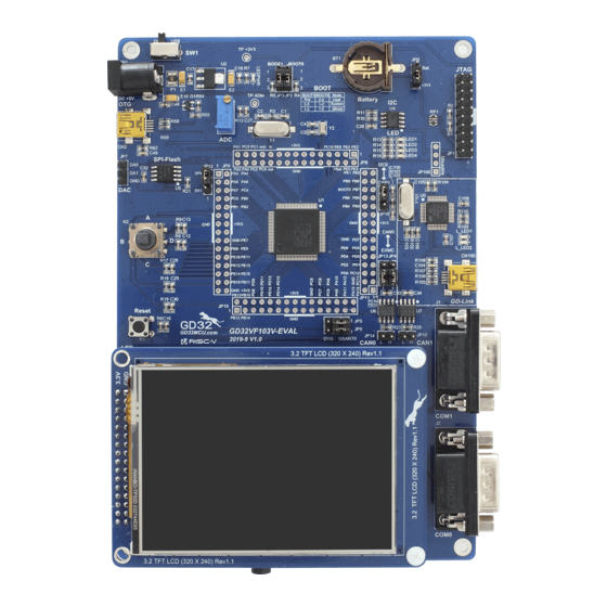
User Guide GD32VF103V-EVAL Summary GD32VF103V-EVAL evaluation board uses GD32VF103VBT6 as the main controller. As a complete development platform of GD32VF103 powered by RISC-V core, the board supports full range of peripherals. It uses mini-USB interface or AC/DC adapter to supply 5V power. -
Page 8: Getting Started
User Guide GD32VF103V-EVAL Function Description CAN1_TX PD14 EXMC_D0 PD15 EXMC_D1 EXMC_D2 EXMC_D3 EXMC_D4 EXMC_D5 EXMC_D6 PE10 EXMC_D7 PE11 EXMC_D8 PE12 EXMC_D9 PE13 EXMC_D10 PE14 EXMC_D11 PE15 EXMC_D12 EXMC_D13 EXMC_D14 PD10 EXMC_D15 EXMC_A23 EXMC_NOE EXMC_NWE EXMC_NE0 ADC01_IN13 DAC_OUT0 DAC_OUT1 Getting started The EVAL board uses Mini USB connecter or DC-005 connector to get power DC +5V, which is the hardware system normal work voltage. -
Page 9: Hardware Layout Overview
User Guide GD32VF103V-EVAL Hardware layout overview 4.1. Power supply Figure 4-1 Schematic diagram of power supply 4.2. Boot option Figure 4-2 Schematic diagram of boot option BOOT0 +3V3 10KΩ BOOT0 10KΩ +3V3 BOOT1 Table 4-1 Boot configuration BOOT1 BOOT0 Boot Mode... -
Page 10: Led
User Guide GD32VF103V-EVAL 4.3. Figure 4-3 Schematic diagram of LED function LED1 LED1 470Ω LED0603 LED2 LED2 470Ω LED0603 LED3 LED3 470Ω LED0603 LED4 LED4 470Ω LED0603 4.4. Figure 4-4 Schematic diagram of Key function +3V3 +3V3 +3V3 +3V3 +3V3... -
Page 11: Usart
User Guide GD32VF103V-EVAL 4.5. USART Figure 4-5 Schematic diagram of USART function USART0/USART1 +3V3 50V/0.1uF MAX3232CSE+ 50V/0.1uF 50V/0.1uF 50V/0.1uF 50V/0.1uF USART1_TX RS232_TX1 T1IN T1OUT USART0_TX RS232_TX0 T2IN T2OUT USART1_RX RS232_RX1 R1OUT R1IN USART0_RX RS232_RX0 R2OUT R2IN COM1 Short JP5(1,2),Short JP6(1,2) for USART0 function... -
Page 12: I2S
User Guide GD32VF103V-EVAL 4.8. Figure 4-8 Schematic diagram of I2S function 10KΩ PB12 I2S0_WS I2S0_SD +3V3 C44 50V/0.1uF SDIN AOUTR PB13 I2S0_CK I2S0_CK 470Ω SCLK I2S0_MCK I2S0_WS 16V/3.3uF,AVX LRCK PB15 I2S0_SD I2S0_MCK MCLK AOUTL FILT+ 470Ω HeadPhone CS4344 16V/3.3uF,AVX 10KΩ... -
Page 13: Can
User Guide GD32VF103V-EVAL 4.11. Figure 4-11 Schematic diagram of CAN function Short JP4(1,2) for EXMC function +3V3 Short JP4(2,3) for CAN0 function CAN0_TX 50V/0.1uF JP14 EXMC_D3 CAN0_TX CAN0_RX CAN0H CANH 120Ω MHDR1X3 CAN0L CANL HEADER 2 Vref Short JP13(1,2) for EXMC function... -
Page 14: Usbfs
User Guide GD32VF103V-EVAL 4.13. USBFS Figure 4-13 Schematic diagram of USBFS function 47KΩ PD13 S8550 470Ω +U5V 16V/10uF,AVX 50V/0.1uF PA9,PA10 are AFIOs, please refer to USART schematic for right config USB_VBUS VBUS PA11 USB_DM PA12 USB_DP PA10 USB_ID Shield Mini_USB 1MΩ... -
Page 15: Gd-Link
User Guide GD32VF103V-EVAL 4.14. GD-Link Figure 4-14 Schematic diagram of GD-Link function PA0-WKUP MCU SWD PB2/BOOT1 PB3/JTDO L_TMS/IO PB4/JNTRST L_TCK/CLK +3V3 JP100 L_TDO/SWO L_TDI L_SWDIO L_SWDCK L_USB_Ctr L_TReset L_LED1 LED0603 PA10 PB10 4× 1P2.54 L_USB_DM PA11 PB11 L_USB_DP L_LED1 R109 470Ω... -
Page 16: Mcu
User Guide GD32VF103V-EVAL 4.16. Figure 4-16 Schematic diagram of MCU Pin PA0-WKUP PA10 PC10 PA10 PC10 PA11 PC11 PA11 PC11 PA12 PC12 PA12 PC12 PA13 PC13 PA13/JTMS/SWDIO PC13-TAMPER-RTC PA14 PC14 PA14/JTCK/SWCLK PC14-OSC32_IN PA15 PC15 PA15/JTDI PC15-OSC32_OUT PB2/BOOT1 PB3/JTDO PB4/JNTRST PB10... -
Page 17: Demo Running Result
Learn to use GPIO for controlling the LED Learn to use SysTick to generate 1ms delay GD32VF103V-EVAL board has four LEDs. The LED1, LED2, LED3 and LED4 are controlled by GPIO. This demo will show how to light the LEDs. 5.1.2. -
Page 18: Demo Running Result
User Guide GD32VF103V-EVAL 5.3.2. DEMO running result Download the program <03_EXTI_Key_Interrupt_mode> to the EVAL board, first of all, all the LEDs will be flashed once for test. Then press down the KEY_B, LED2 will be turned on. Press down the KEY_B again, LED2 will be turned off. -
Page 19: Usart_Dma
User Guide GD32VF103V-EVAL LED3, LED4 toggle together. The output information via the serial port is as following. 5.6. USART_DMA 5.6.1. DEMO purpose This demo includes the following functions of GD32 MCU: Learn to use the USART transmit and receive data using DMA 5.6.2. -
Page 20: Adc_Conversion_Triggered_By_Timer
<07_ADC_conversion_triggered_by_timer> GD32VF103V-EVAL board, adjust the adjustable potentiometer knob to change the analog input. The ADC, which is triggered by TIMER1 CH1 event, will convert the analog input, and you will see the result, a voltage curve, on the LCD. The curve adjusts with the analog input. -
Page 21: Adc0_Adc1_Regular_Parallel_Mode
5.9.2. DEMO running result Download program <09_ADC0_ADC1_Regular_Parallel_mode> GD32VF103V-EVAL board. Connect serial cable to EVAL_COM0, open the HyperTerminal. PA0 and PA3 pin connect to external voltage input. TIMER0_CH0 is the trigger source of ADC0 and ADC1. When the rising edge of... -
Page 22: Dac_Output_Voltage_Value
User Guide GD32VF103V-EVAL TIMER0_CH0 coming, ADC0 and ADC1 convert the regular channel group parallelly. The values of ADC0 and ADC1 are transmitted to array adc_value[0] and adc_value[1] by DMA. When the first rising edge of TIMER0_CH0 coming, the value of the ADC0 conversion of PA0 pin is stored into the low half word of adc_value[0], the value of the ADC1 conversion of PA3 pin is stored into the high half word of adc_value[0]. -
Page 23: Demo Running Result
User Guide GD32VF103V-EVAL 5.10.2. DEMO running result Download the program <10_DAC_Output_Voltage_Value> to the EVAL board, the digital value is 0x7ff0, its converted analog voltage should be VREF/2, using the voltmeter to measure PA4, its value is 1.648V. 5.11. I2C_EEPROM 5.11.1. -
Page 24: Demo Running Result
User Guide GD32VF103V-EVAL 5.12.2. DEMO running result The computer serial port line connected to the COM0 port of development board, set the baud rate of HyperTerminal software to 115200, 8 bits data bit, 1 bit stop bit. At the same time, you should jump the JP12 to SPI, jump JP5 and JP6 to USART. -
Page 25: I2S_Audio_Player
Learn to use I2S module to output audio file GD32VF103V-EVAL board integrates the I2S (Inter-IC Sound) module, and the module can communicate with external devices using the I2S audio protocol. This demo mainly shows how to use the I2S interface of the board for audio output. -
Page 26: Can_Network
DEMO running result This example is tested with two GD32VF103V-EVAL boards. Jump the JP5, JP6 to USART and JP13, JP4 to CAN with the jumper cap. Connect L pin to L pin and H pin to H pin of JP14 on the boards for sending and receiving frames. -
Page 27: Rcu_Clock_Out
User Guide GD32VF103V-EVAL 5.16. RCU_Clock_Out 5.16.1. DEMO purpose This demo includes the following functions of GD32 MCU: Learn to use GPIO control the LED Learn to use the clock output function of RCU Learn to communicate with PC by USART 5.16.2. -
Page 28: Demo Running Result
User Guide GD32VF103V-EVAL 5.17.2. DEMO running result Download the program < 17_PMU_sleep_wakeup > to the EVAL board, connect serial cable to EVAL_COM. After power-on, all the LEDs are off. The MCU will enter sleep mode and the software stop running. When the USART0 receives a byte of data from the HyperTerminal, the MCU will wake up from a receive interrupt. -
Page 29: Timer_Breath_Led
DEMO running result Use the DuPont line to connect the TIMER0_CH0 (PA8) and LED1 (PC0), and then download the program <19_TIMER_Breath_LED> to the GD32VF103V-EVAL board and run. PA8 should not be reused by other peripherals. When the program is running, you can see LED1 lighting from dark to bright gradually and... -
Page 30: Usbfs_Device
User Guide GD32VF103V-EVAL then gradually darken, ad infinitum, just like breathing as rhythm. 5.20. USBFS_Device 5.20.1. CDC_ACM DEMO purpose This demo includes the following functions of GD32 MCU: Learn how to use the USBFS peripheral Learn how to implement USB CDC device EVAL board has one USBFS interface. -
Page 31: Usbfs_Host
Learn to use the USBFS as a HID host Learn the operation between the HID host and the mouse device Learn the operation between the HID host and the keyboard device GD32VF103V-EVAL board integrates the USBFS module, and the module can be used as a... -
Page 32: Msc
Learn the operation between the MSC host and the Udisk GD32VF103V-EVAL board integrates the USBFS module, and the module can be used as a USB device, a USB host or an OTG device. This demo mainly shows how to use the USBFS as a USB MSC host to communicate with external Udisk. -
Page 33: Revision History
User Guide GD32VF103V-EVAL Revision history Table 6-1 Revision history Revision No. Description Date Initial Release Jun.05, 2019 Update the titles of chapter 5.20 and 5.21, update new Sept.18, 2019 logo in EXMC_TouchScreen... - Page 34 Important Notice This document is the property of GigaDevice Semiconductor Inc. and its subsidiaries (the "Company"). This document, including any product of the Company described in this document (the “Product”), is owned by the Company under the intellectual property laws and treaties of the People’s Republic of China and other jurisdictions worldwide.
Need help?
Do you have a question about the GD32VF103V-EVAL and is the answer not in the manual?
Questions and answers