Table of Contents
Advertisement
Quick Links
Advertisement
Table of Contents

Related Manuals for Asus AAEON COM-ADNC6


Summary of Contents for Asus AAEON COM-ADNC6
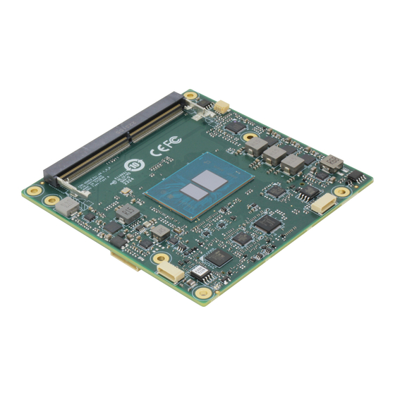
- Page 1 COM-ADNC6 COM Express Module User’s Manual 1 Last Updated: March 1, 2024...
- Page 2 Copyright Notice This document is copyrighted, 2024. All rights are reserved. The original manufacturer reserves the right to make improvements to the products described in this manual at any time without notice. No part of this manual may be reproduced, copied, translated, or transmitted in any form or by any means without the prior written permission of the original manufacturer.
- Page 3 Acknowledgements All other products’ name or trademarks are properties of their respective owners. Microsoft Windows® is a registered trademark of Microsoft Corp. ⚫ Intel® and Atom® are registered trademarks of Intel Corporation. ⚫ Intel® Core™ is a trademark of Intel Corporation. ⚫...
- Page 4 Packing List Before setting up your product, please make sure the following items have been shipped: Item Quantity COM-ADNC6 ⚫ If any of these items are missing or damaged, please contact your distributor or sales representative immediately. Preface...
- Page 5 About this Document This User’s Manual contains all the essential information, such as detailed descriptions and explanations on the product’s hardware and software features (if any), its specifications, dimensions, jumper/connector settings/definitions, and driver installation instructions (if any), to facilitate users in setting up their product. Users may refer to the product page at AAEON.com for the latest version of this document.
- Page 6 Safety Precautions Please read the following safety instructions carefully. It is advised that you keep this manual for future references All cautions and warnings on the device should be noted. Make sure the power source matches the power rating of the device. Position the power cord so that people cannot step on it.
- Page 7 If any of the following situations arises, please the contact our service personnel: Damaged power cord or plug Liquid intrusion to the device iii. Exposure to moisture Device is not working as expected or in a manner as described in this manual The device is dropped or damaged Any obvious signs of damage displayed on the device...
- Page 8 FCC Statement This device complies with Part 15 FCC Rules. Operation is subject to the following two conditions: (1) this device may not cause harmful interference, and (2) this device must accept any interference received including interference that may cause undesired operation.
- Page 9 China RoHS Requirements (CN) 产品中有毒有害物质或元素名称及含量 AAEON Main Board/ Daughter Board/ Backplane 有毒有害物质或元素 部件名称 铅 汞 镉 六价铬 多溴联苯 多溴二苯醚 (Pb) (Hg) (Cd) (Cr(VI)) (PBB) (PBDE) 印刷电路板 ○ ○ ○ ○ 及其电子组件 外部信号 ○ ○ ○ ○ 连接器及线材 O:表示该有毒有害物质在该部件所有均质材料中的含量均在 SJ/T 11363-2006 标准规定的限量要求以下。 X:表示该有毒有害物质至少在该部件的某一均质材料中的含量超出...
- Page 10 China RoHS Requirement (EN) Poisonous or Hazardous Substances or Elements in Products AAEON Main Board/ Daughter Board/ Backplane Poisonous or Hazardous Substances or Elements Hexavalent Polybrominated Polybrominated Component Lead Mercury Cadmium Chromium Biphenyls Diphenyl Ethers (Pb) (Hg) (Cd) (Cr(VI)) (PBB) (PBDE) PCB &...
-
Page 11: Table Of Contents
Table of Contents Chapter 1 - Product Specifications..................1 Specifications ......................2 Block Diagram ......................5 Chapter 2 – Hardware Information ..................6 Dimensions ....................... 7 Jumpers and Connectors ..................10 List of Connectors ....................12 2.3.1 MP2960GQKT-000C-W Download Port (PJPM1) ......... 13 2.3.2 SPI ROM Flash Tool (JSPI1) ................ - Page 12 3.4.8.1 Serial Port 1 Configuration ............37 3.4.8.2 Serial Port 2 Configuration ............38 3.4.9 Serial Port Console Redirection .............. 39 3.4.10 Legacy Console Redirection Settings ............ 40 3.4.11 AAEON BIOS Robot ...................41 3.4.12 On-Module Configuration ............... 43 3.4.13 Power Management .................. 44 3.4.14 GPIO Port Configuration ................
- Page 13 I/O Address Map ....................71 Memory Address Map ..................73 IRQ Mapping Chart ....................74 Preface XIII...
-
Page 14: Chapter 1 - Product Specifications
Chapter 1 Chapter 1 - Product Specifications... -
Page 15: Specifications
Specifications System Form Factor COM Express, Type 6 Intel Atom® X Series/N-series/Core™ i3-N305 CPU Intel® Core™ i3-N305 (8C, up to 3.8 GHz, 15W) Intel Atom® x7425E (4C, up to 3.4 GHz, 12W) Intel Atom® x7211E (2C, up to 3.2 GHz, 6W) Intel®... - Page 16 Display Graphics Controller Intel® UHD Graphics Video Output 3 Displays: 18/24-bit Single/Dual-Channel LVDS/eDP x 1, up to 1920 x 1080/3840 x 2160 DP x 2, up to 3840 x 2160 @144Hz Ethernet Intel® Ethernet Controller I226-V or I226-IT 2.5GbE x 1 Audio High Definition Audio Interface USB Port...
- Page 17 Environmental Weight 0.26 lb. (0.12Kg) Chapter 1 – Product Specifications...
-
Page 18: Block Diagram
Block Diagram Chapter 1 – Product Specifications... -
Page 19: Chapter 2 - Hardware Information
Chapter 2 Chapter 2 – Hardware Information... -
Page 20: Dimensions
Dimensions Component Side Chapter 2 – Hardware Information... - Page 21 Solder Side Chapter 2 – Hardware Information...
- Page 22 With Active Cooler With Heatspreader With Active Cooler and Heatspreader Chapter 2 – Hardware Information...
-
Page 23: Jumpers And Connectors
Jumpers and Connectors Component Side Chapter 2 – Hardware Information... - Page 24 Solder Side Chapter 2 – Hardware Information...
-
Page 25: List Of Connectors
List of Connectors Please refer to the table below for all of the board’s connectors that you can configure for your application Label Function PJPM1 MP2960GQKT-000C-W Download Port JSPI1 SPI ROM Flash Tool JSPI2 I226 ROM Flash Tool CN18 Debug Port 80 COMAB1 Type 6 Row A/B COMCD1... -
Page 26: Mp2960Gqkt-000C-W Download Port (Pjpm1)
2.3.1 MP2960GQKT-000C-W Download Port (PJPM1) Signal Signal 2.3.2 SPI ROM Flash Tool (JSPI1) Signal Signal SPI MISO SPI CLK +V3P3A SPI MOSI SPI CS0# 2.3.3 I226 ROM Flash Tool (JSPI2) Signal Signal SPI MISO SPI CLK +V3P3A SPI MOSI SPI CS0# Chapter 2 –... -
Page 27: Debug Port 80 (Cn18)
2.3.4 Debug Port 80 (CN18) Signal Signal LPC_AD0 LPC_AD1 LPC_AD2 LPC_AD3 +V3P3A LPC_FRAME# BUF_PLT_RST# CLK_PCI_DEBUG 2.3.5 Type 6 Row A/B (COMAB1) Row A Row B Signal Signal GBE0_MDI3- GBE0_ACT# GBE0_MDI3+ LPC_FRAME#/ESPI_CS0# GBE0_LINK100# LPC_AD0/ESPI_IO_0 GBE0_LINK1000# LPC_AD1/ESPI_IO_1 GBE0_MDI2- LPC_AD2/ESPI_IO_2 GBE0_MDI2+ LPC_AD3/ESPI_IO_3 GBE0_LINK# LPC_DRQ0#/ESPI_ALERT0#(NC) GBE0_MDI1- LPC_DRQ1#/ESPI_ALERT1#(NC) - Page 28 Row A Row B Signal Signal SATA0_TX+ SATA1_TX+ SATA0_TX- SATA1_TX- SUS_S4# SUS_STAT#/ESPI_RESET# SATA0_RX+ SATA1_RX+ SATA0_RX- SATA1_RX- SATA2_TX+(NC) SATA3_TX+(NC) SATA2_TX-(NC) SATA3_TX-(NC) SUS_S5# PWR_OK SATA2_RX+(NC) SATA3_RX+(NC) SATA2_RX-(NC) SATA3_RX-(NC) BATLOW# (S)ATA_ACT# HDA_SDIN2/SNDW0_CLK(NC) HDA_SYNC HDA_SDIN1/SNDW0_DAT HDA_RST# HDA_SDIN0 HDA_BITCLK SPKR HDA_SDOUT I2C_CK BIOS_DIS0#/ESPI_SAFS I2C_DAT THRMTRIP# THRM# USB6- USB7-...
- Page 29 Row A Row B Signal Signal USB2+ USB3+ USB_2_3_OC# USB_0_1_OC# USB0- USB1- USB0+ USB1+ VCC_RTC ESPI_EN# RSMRST_OUT# USB0_HOST_PRSNT(NC) GBE0_SDP SYS_RESET# LPC_SERIRQ/ESPI_CS1# CB_RESET# PCIE_TX5+(NC) PCIE_RX5+(NC) PCIE_TX5-(NC) PCIE_RX5-(NC) GPI0 GPO1 PCIE_TX4+(NC) PCIE_RX4+(NC) PCIE_TX4-(NC) PCIE_RX4-(NC) GPO2 PCIE_TX3+ PCIE_RX3+ PCIE_TX3- PCIE_RX3- PCIE_TX2+ PCIE_RX2+ PCIE_TX2- PCIE_RX2- GPI1 GPO3...
- Page 30 Row A Row B Signal Signal LVDS_A0+ LVDS_B0+ LVDS_A0- LVDS_B0- LVDS_A1+ LVDS_B1+ LVDS_A1- LVDS_B1- LVDS_A2+ LVDS_B2+ LVDS_A2- LVDS_B2- LVDS_VDD_EN LVDS_B3+ LVDS_A3+ LVDS_B3- LVDS_A3- LVDS_BKLT_EN LVDS_A_CK+ LVDS_B_CK+ LVDS_A_CK- LVDS_B_CK- LVDS_I2C_CK LVDS_BKLT_CTLR LVDS_I2C_DAT VCC_5V_SBY_0 GPI3 VCC_5V_SBY_1 GP_SPI_MOSI VCC_5V_SBY_2 eDP_HPD VCC_5V_SBY_3 PCIE0_CK_REF+ BIOS_DIS1# PCIE0_CK_REF- VGA_RED(NC) SPI_POWER...
-
Page 31: Type 6 Row C/D (Comcd1)
Row A Row B Signal Signal TYPE10#(NC) SPI_CS# RS1_TX GP_SPI_MISO RS1_RX GP_SPI_CK A100 B100 A101 RS2_TX B101 FAN_PWMOUT A102 RS2_RX B102 FAN_TACHIN A103 LID# B103 SLEEP# A104 VCC_12V_0 B104 VCC_12V_6 A105 VCC_12V_1 B105 VCC_12V_7 A106 VCC_12V_2 B106 VCC_12V_8 A107 VCC_12V_3 B107 VCC_12V_9 A108... - Page 32 Row C Row D Signal Signal USB_SSRX2-(NC) USB_SSTX2-(NC) USB_SSRX2+(NC) USB_SSTX2+(NC) USB_SSRX3-(NC) USB_SSTX3-(NC) USB_SSRX3+(NC) USB_SSTX3+(NC) DDI1_CTRLCLK_AUX+/USB4_1_ USB4_1_LSTX(NC) AUX+ DDI1_CTRLDATA_AUX-/USB4_1 USB4_1_LSRX(NC) _AUX- USB4_RT_ENA(NC) USB4_PD_I2C_ALERT#(NC) RSVD(GND) PMCALERT# PCIE_RX6+(NC) PCIE_TX6+(NC) PCIE_RX6-(NC) PCIE_TX6-(NC) PCIE_RX7+(NC) PCIE_TX7+(NC) PCIE_RX7-(NC) PCIE_TX7-(NC) DDI1_HPD RSVD(GND) SML0_CLK RSVD(GND) SML0_DAT DDI1_PAIR0+/USB4_1_SSTX0+ SML1_CLK DDI1_PAIR0-/USB4_1_SSTX0- SML1_DAT GND_50(NC) USB4_PD_I2C_CLK(NC)
- Page 33 Row C Row D Signal Signal USB4_2_LSTX(NC) USB4_2_LSRX(NC) DDI3_CTRLCLK_AUX+(NC) DDI1_PAIR3+/USB4_1_SSRX1+ DDI3_CTRLDATA_AUX-(NC) DDI1_PAIR3-/USB4_1_SSRX1- DDI3_DDC_AUX_SEL(NC) RSVD(GND) DDI3_PAIR0+(NC) DDI2_PAIR0+/USB4_2_SSTX0+ DDI3_PAIR0-(NC) DDI2_PAIR0-/USB4_2_SSTX0- DDI3_PAIR1+(NC) DDI2_PAIR1+/USB4_2_SSRX0+ DDI3_PAIR1-(NC) DDI2_PAIR1-/USB4_2_SSRX0- DDI3_HPD(NC) DDI2_HPD GP_SPI_CS# RSVD(GND) DDI3_PAIR2+(NC) DDI2_PAIR2+/USB4_2_SSTX1+ DDI3_PAIR2-(NC) DDI2_PAIR2-/USB4_2_SSTX1- RSVD_6(NC) RSVD(GND) DDI3_PAIR3+(NC) DDI2_PAIR3+/USB4_2_SSRX1+ DDI3_PAIR3-(NC) DDI2_PAIR3-/USB4_2_SSRX1- PEG_RX0+(NC) PEG_TX0+(NC) PEG_RX0-(NC) PEG_TX0-(NC) TYPE0#(NC) PEG_LANE_RV#(NC) PEG_RX1+(NC)
- Page 34 Row C Row D Signal Signal PEG_RX3-(NC) PEG_TX3-(NC) RSVD(GND) RSVD(GND) RSVD(GND) RSVD(GND) PEG_RX4+(NC) PEG_TX4+(NC) PEG_RX4-(NC) PEG_TX4-(NC) RAPID_SHUTDOWN PEG_RX5+(NC) PEG_TX5+(NC) PEG_RX5-(NC) PEG_TX5-(NC) PEG_RX6+(NC) PEG_TX6+(NC) PEG_RX6-(NC) PEG_TX6-(NC) PEG_RX7+(NC) PEG_TX7+(NC) PEG_RX7-(NC) PEG_TX7-(NC) RSVD(GND) RSVD(GND) PEG_RX8+(NC) PEG_TX8+(NC) PEG_RX8-(NC) PEG_TX8-(NC) PEG_RX9+(NC) PEG_TX9+(NC) PEG_RX9-(NC) PEG_TX9-(NC) RSVD(GND) RSVD(GND) PEG_RX10+(NC) PEG_TX10+(NC)
- Page 35 Row C Row D Signal Signal PEG_RX11-(NC) PEG_TX11-(NC) PEG_RX12+(NC) PEG_TX12+(NC) PEG_RX12-(NC) PEG_TX12-(NC) PEG_RX13+(NC) PEG_TX13+(NC) PEG_RX13-(NC) PEG_TX13-(NC) RSVD(GND) RSVD(GND) PEG_RX14+(NC) PEG_TX14+(NC) PEG_RX14-(NC) PEG_TX14-(NC) C100 D100 C101 PEG_RX15+(NC) D101 PEG_TX15+(NC) C102 PEG_RX15-(NC) D102 PEG_TX15-(NC) C103 D103 C104 VCC_12V_0 D104 VCC_12V_6 C105 VCC_12V_1 D105 VCC_12V_7 C106...
-
Page 36: Chapter 3 - Ami Bios Setup
Chapter 3 Chapter 3 - AMI BIOS Setup... -
Page 37: System Test And Initialization
System Test and Initialization These routines test and initialize board hardware. If the routines encounter an error during the tests, you will either hear a few short beeps or see an error message on the screen. There are two kinds of errors: fatal and non-fatal. The system can usually continue the boot up sequence with non-fatal errors. -
Page 38: Ami Bios Setup
AMI BIOS Setup The AMI BIOS ROM has a built-in Setup program that allows users to modify the basic system configuration. This information is stored in the battery-backed CMOS RAM and BIOS NVRAM so it retains the Setup information when the power is turned off. To enter Setup, power on the computer and press <Del>... -
Page 39: Setup Submenu: Main
Setup Submenu: Main Chapter 3 – AMI BIOS Setup... -
Page 40: Setup Submenu: Advanced
Setup Submenu: Advanced Chapter 3 – AMI BIOS Setup... -
Page 41: Cpu Configuration
3.4.1 CPU Configuration Options Summary Intel (VMX) Virtualization Disabled Technology Enabled Optimal Default, Failsafe Default When enabled, a VMM can utilize the additional hardware capabilities provided by Vanderpool Technology. Intel® SpeedStep™ Disabled Enabled Optimal Default, Failsafe Default Allows more than two frequency ranges to be supported. Turbo Mode Disabled Enabled... -
Page 42: Pch-Fw Configuration
3.4.2 PCH-FW Configuration Chapter 3 – AMI BIOS Setup... -
Page 43: Firmware Update Configuration
3.4.3 Firmware Update Configuration Options Summary Me FW Image Re-Flash Enabled Disabled Optimal Default, Failsafe Default Enable/Disable Me FW Image Re-Flash function. FW Update Disabled Enabled Optimal Default, Failsafe Default Enable/Disable ME FW Update function. Chapter 3 – AMI BIOS Setup... -
Page 44: Ptt Configuration
3.4.4 PTT Configuration Options Summary TPM Device Selection dTPM Optimal Default, Failsafe Default Selects TPM device: PTT or discrete TPM. PTT - enables PTT in SkuMgr dTPM - disables PTT is SkuMgr Warning! PTT/dTPM will be disabled and all data saved on it will be lost. Chapter 3 –... -
Page 45: Trusted Computing
3.4.5 Trusted Computing Options Summary Security Device Support Enable Optimal Default, Failsafe Default Disable Enables or Disables BIOS support for security device. O.S. will not show Security Device. TCG EFI protocol and INT1A interface will not be available. SHA256 PCR Bank Enabled Optimal Default, Failsafe Default Disabled... - Page 46 Options Summary Platform Hierarchy Enabled Optimal Default, Failsafe Default Disabled Enable or Disable Platform Hierarchy Storage Hierarchy Enabled Optimal Default, Failsafe Default Disabled Enable or Disable Storage Hierarchy Endorsement Hierarchy Enabled Optimal Default, Failsafe Default Disabled Enable or Disable Endorsement Hierarchy Physical Presence Spec Optimal Default, Failsafe Default Version...
-
Page 47: Sata Configuration
3.4.6 SATA Configuration Options Summary SATA Controller(s) Enabled Optimal Default, Failsafe Default Disabled Enable/Disable SATA Device. Port 0 Enabled Optimal Default, Failsafe Default Disabled Enable or Disable SATA Port. Port1 Enabled Optimal Default, Failsafe Default Disabled Enable or Disable SATA Port. Chapter 3 –... -
Page 48: On-Module Hardware Monitor
3.4.7 On-Module Hardware Monitor Options Summary System Fan Full Mode Manual Mode Auto – Slope Linear Optimal Default, Failsafe Default PWM signal Non-inverting Optimal Default, Failsafe Default Inverting Select output PWM of inverting or non-uninverting signal. Thermal Monitoring System Temperature Optimal Default, Failsafe Default System Temperature 2 Monitoring thermal sensor select. -
Page 49: Sio Configuration
Options Summary Slope (PWM) 0 (PWM) 1 (PWM) Optimal Default, Failsafe Default 2 (PWM) 4 (PWM) 8 (PWM) 16 (PWM) 32 (PWM) 64 (PWM) When the monitored temperature is higher than the Start-Up temperature, the PWM output increases per degree. 3.4.8 SIO Configuration Chapter 3 –... -
Page 50: Serial Port 1 Configuration
3.4.8.1 Serial Port 1 Configuration Options Summary Use This Device Disable Enable Optimal Default, Failsafe Default Enable or Disable this Logical Device. Possible: Use Automatic Settings Optimal Default, Failsafe Default IO=3F8h; IRQ=4 IO=2C8h; IRQ=11 Allows user to change Device's Resource settings. New settings will be reflected on This Setup Page after System restarts. -
Page 51: Serial Port 2 Configuration
3.4.8.2 Serial Port 2 Configuration Options Summary Use This Device Disable Enable Optimal Default, Failsafe Default Enable or Disable this Logical Device. Possible: Use Automatic Settings Optimal Default, Failsafe Default IO=2F8h; IRQ=3 IO=3D8h; IRQ=10 Allows user to change Device's Resource settings. New settings will be reflected on This Setup Page after System restarts. -
Page 52: Serial Port Console Redirection
3.4.9 Serial Port Console Redirection Options Summary Console Redirection Disabled Optimal Default, Failsafe Default Enabled Console Redirection Enable or Disable. Console Redirection EMS Disabled Optimal Default, Failsafe Default Enabled Console Redirection Enable or Disable. Chapter 3 – AMI BIOS Setup... -
Page 53: Legacy Console Redirection Settings
3.4.10 Legacy Console Redirection Settings Options Summary Redirection COM port COM0 Optimal Default, Failsafe Default COM1(Pci Bus0, Dev0, Func0) (Disabled) Select a COM Port to display redirection of Legacy OS and Legacy OPROM message. Resolution 80x24 Optimal Default, Failsafe Default 80x25 On Legacy OS, the number of Rows and Columns supported redirection. -
Page 54: Aaeon Bios Robot
3.4.11 AAEON BIOS Robot Options Summary Sends watch dog before Disabled Optimal Default, Failsafe Default BIOS POST Enabled Enabled - Robot set Watch Dog Timer (WDT) right after power on, before BIOS start POST process. And then Robot will clear WDT on completion of POST. WDT will reset system automatically if it is not cleared before its timer counts down to zero. - Page 55 Options Summary OS Timer (minute) Optimal Default, Failsafe Default Timer count set to Watch Dog Timer for OS loading. Delayed POST (PEI phase) Disabled Optimal Default, Failsafe Default Enabled Enabled - Robot holds BIOS from starting POST, right after power on. This allows BIOS POST to start with stable power or start after system is physically warmed-up.
-
Page 56: On-Module Configuration
3.4.12 On-Module Configuration Options Summary Battery Management Disabled Optimal Default, Failsafe Default Enabled Enable to support battery in ACPI OS by I2C_CK, I2C_DAT(B33,B44). EC-SMB-HC Support Disabled Optimal Default, Failsafe Default Enabled SMBus Host Controller Interface via Embedded Controller by (B33, B34). Chapter 3 –... -
Page 57: Power Management
3.4.13 Power Management Options Summary Power Mode ATX Type Optimal Default, Failsafe Default AT Type Select power supply mode. Restore AC Power Loss Last State Always On Always Off Optimal Default, Failsafe Default Select power state when power is re-applied after a power failure. Soft-Off (S5) Wake On RTC Disable Optimal Default, Failsafe Default By Date... -
Page 58: Gpio Port Configuration
3.4.14 GPIO Port Configuration Options Summary GPIO Port* Output Input Set GPIO as Input or Output. Output Level High Set output level when GPIO pin is output. Chapter 3 – AMI BIOS Setup... -
Page 59: Setup Submenu: Chipset
Setup Submenu: Chipset Chapter 3 – AMI BIOS Setup... -
Page 60: System Agent (Sa) Configuration
3.5.1 System Agent (SA) Configuration Options Summary VT-d Disabled Optimal Default, Failsafe Default Enabled VT-d capability. Chapter 3 – AMI BIOS Setup... -
Page 61: Memory Configuration
3.5.2 Memory Configuration Chapter 3 – AMI BIOS Setup... -
Page 62: Lvds Panel Configuration
3.5.3 LVDS Panel Configuration Options Summary LVDS Disabled Enabled Optimal Default, Failsafe Default Enable/Disabled this panel. LVDS Panel Type 640x480,18bit,60Hz 800x480,18bit,60Hz 800x600,18bit,60Hz 1024x600,18bit,60Hz 1024x768,18bit,60Hz 1024x768,24bit,60Hz Optimal Default, Failsafe Default 1280x768,24bit,60Hz 1280x1024,48bit,60Hz 1366x768,24bit,60Hz 1440x900,48bit,60Hz 1600x1200,48bit,60Hz 1920x1080,48bit,60Hz Chapter 3 – AMI BIOS Setup... - Page 63 Options Summary LVDS Panel Type (cont.) 1920x1200,48bit,60Hz Select LCD panel used by Internal Graphics Device by selecting the appropriate setup item. Color Depth 18-bit Optimal Default, Failsafe Default 24-bit 36-bit 48-bit Select panel type. Backlight Type Normal Optimal Default, Failsafe Default Inverted Select backlight control signal type.
-
Page 64: Pch-Io Configuration
3.5.4 PCH-IO Configuration Options Summary HD Audio Disabled Enabled Optimal Default, Failsafe Default Control Detection of the HD-Audio device. Disable = HAD will be unconditionally disabled Enable = HAD will be unconditionally enabled. Chapter 3 – AMI BIOS Setup... -
Page 65: Hsio Configuration
3.5.5 HSIO Configuration Options Summary PCIe Controller 1 Override Disabled Optimal Default, Failsafe Default Enabled HSIO PCIe Controller override. PCIe Controller 1 Setting PCIE Controller are four Optimal Default, Failsafe Default PCIE Controller are two PCIe Controller Setting. PCIe Controller 1 Reversal Non-Reversed Optimal Default, Failsafe Default Reversed... - Page 66 Options Summary PCIe Controller 3 Setting PCIE Controller are four Optimal Default, Failsafe Default PCIE Controller are two PCIe Controller Setting. PCIe Controller 3 Reversal Non-Reversed Optimal Default, Failsafe Default Reversed PCIE LANE REVERSAL. Chapter 3 – AMI BIOS Setup...
-
Page 67: Pci Express Configuration
3.5.5.1 PCI Express Configuration Chapter 3 – AMI BIOS Setup... -
Page 68: Pci Express Root Port 3
3.5.5.2 PCI Express Root Port 3 Options Summary PCIe Speed Auto Optimal Default, Failsafe Default Gen 1 Gen 2 Gen 3 Configure PCIe Speed. Hot Plug Disabled Optimal Default, Failsafe Default Enabled PCI Express Hot Plug Enable/Disable. Chapter 3 – AMI BIOS Setup... -
Page 69: Pci Express Root Port 4
3.5.5.3 PCI Express Root Port 4 Options Summary PCIe Speed Auto Optimal Default, Failsafe Default Gen 1 Gen 2 Gen 3 Configure PCIe Speed. Hot Plug Disabled Optimal Default, Failsafe Default Enabled PCI Express Hot Plug Enable/Disable. Chapter 3 – AMI BIOS Setup... -
Page 70: Pci Express Root Port 9
3.5.5.4 PCI Express Root Port 9 Options Summary PCIe Speed Auto Optimal Default, Failsafe Default Gen 1 Gen 2 Gen 3 Configure PCIe Speed. Hot Plug Disabled Optimal Default, Failsafe Default Enabled PCI Express Hot Plug Enable/Disable. Chapter 3 – AMI BIOS Setup... -
Page 71: Pci Express Root Port 10
3.5.5.5 PCI Express Root Port 10 Options Summary PCIe Speed Auto Optimal Default, Failsafe Default Gen 1 Gen 2 Gen 3 Configure PCIe Speed. Hot Plug Disabled Optimal Default, Failsafe Default Enabled PCI Express Hot Plug Enable/Disable. Chapter 3 – AMI BIOS Setup... -
Page 72: Setup Submenu: Security
Setup Submenu: Security Change Administrator/User Password You can set an Administrator password. If you set an Administrator password, you can then set a User password. User passwords do not have access to many of the features in the Setup utility. Select the password you want to set and press <Enter>. -
Page 73: Secure Boot
3.6.1 Secure Boot Options Summary Secure Boot Disabled Optimal Default, Failsafe Default Enabled Secure Boot feature is Active if Secure Boot is Enabled, Platform Key (PK) is enrolled and the System is in User mode. The mode change requires platform reset. Secure Boot Mode Custom Optimal Default, Failsafe Default... -
Page 74: Key Management
3.6.2 Key Management Options Summary Factory Key Provision Disabled Optimal Default, Failsafe Default Enabled Secure Boot feature is Active if Secure Boot is Enabled, Platform Key (PK) is enrolled and the System is in User mode. The mode change requires platform reset. Restore Factory Keys Force System to User Mode. - Page 75 Options Summary Device Guard ready system must not list 'Microsoft UEFI CA' Certificate in Authorized Signature database (db). Restore DB defaults Restore DB variable to factory defaults. Platform Key (PK) Details Export Update Delete Key Exchange Keys Details Export Update Append Delete Authorized Signatures...
-
Page 76: Setup Submenu: Boot
Setup Submenu: Boot Options Summary Quiet Boot Disabled Enabled Optimal Default, Failsafe Default Enable or Disable Quiet Boot option. UEFI PXE Support Disabled Optimal Default, Failsafe Default Enabled Enable/Disable UEFI Network Stack. FIXED BOOT ORDER Priorities Sets the system boot order. Chapter 3 –... -
Page 77: Bbs Priorities
3.7.1 BBS Priorities Chapter 3 – AMI BIOS Setup... -
Page 78: Setup Submenu: Save & Exit
Setup Submenu: Save & Exit Options Summary Save Changes and Reset Reset the system after saving the changes. Discard Changes and Exit Exit system setup without saving any changes. Restore Defaults Restore/Load Default values for all the setup options. Chapter 3 – AMI BIOS Setup... -
Page 79: Chapter 4 - Drivers Installation
Chapter 4 Chapter 4 – Drivers Installation... -
Page 80: Drivers Download And Installation
Drivers Download and Installation Drivers for the COM-ADNC6 can be downloaded from the product page on the AAEON website by following this link: https://www.aaeon.com/en/p/com-express-cpu-modules-com-adnc6 Download the driver(s) you need and follow the steps below to install them. Chipset Driver Open the folder where you unzipped the Chipset Drivers Run the SetupChipset.exe file in the folder Follow the instructions Drivers will be installed automatically... - Page 81 Install Audio Drivers Note: Ensure Intel Smart Sound Driver (Intel_SST_ADL_v10.29.00.8467) is installed before the Realtek Audio driver (Realtek Audio 6.0.9034.2) Install Intel Smart Sound Driver Open the Audio folder Open the Intel(R)_SST_ADL_v10.29.00.8467 subfolder Follow the setup information within the file to manually install driver. Install Realtek Audio Driver Open the Audio folder Open the Realtek Audio 6.0.9034.2 folder...
- Page 82 Install ME Driver Open the ME folder Run the SetupME.exe file in the folder Follow the instructions Drivers will be installed automatically Chapter 4 – Driver Installation...
-
Page 83: Appendix A - I/O Information
Appendix A Appendix A - I/O Information... - Page 84 I/O Address Map Appendix A – I/O Information...
- Page 85 Appendix A – I/O Information...
- Page 86 A.2 Memory Address Map Appendix A – I/O Information...
- Page 87 A.3 IRQ Mapping Chart Appendix A – I/O Information...
- Page 88 Appendix A – I/O Information...
- Page 89 Appendix A – I/O Information...
Need help?
Do you have a question about the AAEON COM-ADNC6 and is the answer not in the manual?
Questions and answers