
Related Manuals for Bose L1 II


Summary of Contents for Bose L1 II
- Page 1 Model II System ® Power Stand, Cylindrical Radiator and B1 Bass Module ® US/Canada, European, UK and Australian Versions ©2019 Bose Corporation Service Manual Reference Number 296133-SM Rev. 06...
-
Page 2: Table Of Contents
Contents Safety Information ..........................3 Warranty .............................3 Specifications ..........................4-5 Electrostatic Discharge Sensitive (ESDS) Device Handling ............5 Part List Notes ...........................5 Product Description ........................6-9 System Components.........................6 Setting up the L1 model II power stand ..................7 ® Assembling the L1 model II Cylindrical Radiator loudspeaker ...........7 ®... -
Page 3: Safety Information
THE BOSE PRODUCT, AND SHALL NOT BE REPRODUCED OR USED FOR ANY OTHER PURPOSE. Warranty The Bose L1 Model II Power Stand is covered by a limited 2-year transferable warranty. The L1 Model II Cylindrical Radiator and the B1 bass module are covered by a 5-year limited warranty. -
Page 4: Specifications
Specifications External Dimensions Cylindrical Radiator Height: 2070 mm Width: 89 mm Depth: 120 mm ® Power Stand: Height: 110 mm Width: 200 mm Depth: 660 mm (Legs Folded) Bass Module: Height: 380 mm Width: 260 mm Depth: 450 mm ± 10 mm Weight Cylindrical Radiator: 15 lbs (6.8 kg) each section. -
Page 5: Electrostatic Discharge Sensitive (Esds) Device Handling
Specifications Power Amplifiers (All measured using AES17 20kHz Filter Line Input 1,2) Description System State Specification Power @ THD = 1% Vin = Approx 1V (0dBV) 240W Min, 250W Nom. Gain – Vin req’d for 250W into 4 Ohm Vin = Approx 1V (0dBV) 1dBV +/-0.5dB THD @ Full Power –3dB (125W/4Ohm) Vin = Approx 3dBV,... -
Page 6: Product Description
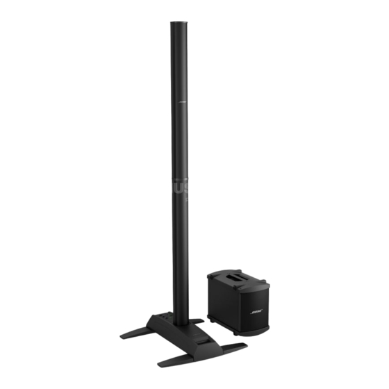
Carrying case AC power cord Carrying bags Bass module cable (blue 4-wire) Demonstration CD Quick setup guide Owner’s guide B1 bass module owner’s guide Model II System with ToneMatch port Owner’s Guide Bass Module Installation Guide www.Bose.com/musicians Product registration card... -
Page 7: Setting Up The L1 ® Model Ii Power Stand
Setting up the L1 model II power stand ® 1. Holding the power stand vertically on the floor (Figure A), grasp one leg and swing it out as far as it will go. Notice that the other legs swing out automatically. The legs must be fully open before you can plug the L1 Cylindrical Radiator bottom section into the power ®... -
Page 8: Connecting The B1 Bass Module
Connecting the B1 bass module You can place the B1 bass module either vertically or horizontally on the floor. Normal placement is between the legs of the power stand. 1. Plug one end of the B1 bass module cable into one of the B1 B1 bass connectors. -
Page 9: Setting The Analog Input Level On The L1 Model Ii Power Stand
Setting the Analog Input Level on the L1 Model II Power Stand ® When connecting an audio source to the Analog Input, follow these steps to adjust the input Trim control. 1. Set the Trim control on the power stand to the 0 (zero) position. 2. -
Page 10: Packaging Part List, L1 Model Ii Power Stand (See Figure 1)
Packaging Part List Model II Power Stand (see Figure 1) ® ® Item Description Bose Part Vendor Part Qty. Note Number Number Number Carton Kit, 307728 Includes items 1, 2 and 3 Carton Sheet, 770x340x6 304982 1450-9300+1 Filler, Corner, Card, 440x170x6... -
Page 11: Packaging Part List, L1 Model Ii Line Array (See Figure 2)
Packaging Part List Model II Line Array (see Figure 2) ® ® Item Description Bose Part Vendor Part Qty. Note Number Number Number Carton Kit, 307721 includes items 1 - 6 Card Sheet 307720 1450-9370+1 Filler, PE, Type 1 307716... -
Page 12: Packaging Part List, B1 Bass Module (See Figure 3)
Packaging Part List B1 Bass Module (see Figure 3) ® Item Description Vendor Part Number Note Bose Part Number Number CUSHION, PACKING 303838 1491-7231+0 BAG, POLY, 12 X 16 X 49” 1497-4552+0 BASS MODULE 032494 CARTON 303837 145B-3030+1 BUBBLE BAG 1497-1122+0 SPEAKER CABLE, L=1.5M... -
Page 13: Main Part List, Power Stand To Leg Assembly (See Figure 4)
Main Part List Power Stand to Leg Assembly (see Figure 4) ® Item Description Bose Part Vendor Part Number Qty. Note Number Number UPPER HOUSING ASSEMBLY 298051 1467-7901+0 LEG ASSEMBLY 304129 SVC-PS211+LEGASY SCREW, MACHINE, FLAT-CS, 2901-4012+3000 M4X12, BZ LABEL, PRODUCT... -
Page 14: Main Part List, L1 Model Ii Power Stand Upper Housing (See Figure 5)
Main Part List Model II Power Stand Upper Housing (see Figure 5) ® ® Item Description Bose Part Vendor Part Number Qty. Note Number Number HOUSING, UPPER 298051 1467-7901+0 I / O PANEL ASSY, 304130 SVC-PS211+IOPAN US/CAN (ITEMS 2 TO 15 AND 32) - Page 15 Figure 5. Power Stand Upper Housing Exploded View...
-
Page 16: Main Part List, L1 Model Ii Power Stand Cavity And Leg Assembly (See Figure 6)
Main Part List Model II Power Stand Cavity and Leg Assembly (see Figure 6) ® ® Item Description Bose Part Vendor Part Number Qty. Note Number Number LEG ASSEMBLY, INCLUDES: 304129 SVC-PS211+LEGASY LEG-1 4135-6821+0 FOOT 4157-1191+0 WASHER, METAL, M4X0.8X10 2600-4008+1003... - Page 17 Figure 6. Power Stand Cavity and Leg Assembly Exploded View...
-
Page 18: Main Part List, L1 Model Ii Line Array (See Figure 7)
2.75” DRIVER, GR, 6 OHM 303836 SVC-WF+BSPAL2 SCREW, MACH, M3.5X8, 6.7MM 2940-3508+3000 GRILLE, UPPER SECTION, 298024-01 4135-6852+1 NO LOGO BOSE LOGO 303709 2150-7012+0 WIRE, 4P, P5.08, #20, UL1007 7012-8530+0 HOUSING, UPPER SECTION 1406-1801+0 SCREW, MACH, OVAL-CS, M6X20 2902-6020+3000 BAYONET, LINE SOURCE... - Page 19 LOWER ARRAY UPPER ARRAY SECTION SECTION END CAP #3 ASSEMBLY END CAP #1 ASSEMBLY 11 12 13 21 22 END CAP #4 ASSEMBLY END CAP #2 ASSEMBLY Figure 7. L1 Model II Line Array Exploded View ®...
-
Page 20: Main Part List, L1 Model Ii Line Array End Cap Assemblies (See Figure 8)
Main Part List Model II Line Array End Cap Assemblies (see Figure 8) ® ® Item Description Bose Vendor Part Qty. Note Number Part Number Number END CAP #1 ASSEMBLY 304133 SVC-L211- ENDCAP1 MS SCREW, M3X12, CSH.BK 2901-3012+3000 SCREW, B-TITE, FLAT-CS, M3X10... - Page 21 END CAP # 1 ASSY END CAP # 2 ASSY END CAP # 3 ASSY DRIVER BAFFLE ASSY END CAP # 4 ASSY Figure 8. L1 Model II Line Array End Cap Assemblies Exploded View ®...
-
Page 22: Main Part List, B1 Bass Module Exploded View (See Figure 9)
Main Part List B1 Bass Module Exploded View (see Figure 9) Item Description Bose Vendor Part Number Note Number Part Number Screw, M4 X 28, BK, B1 Grille 275465 2908-4028+3400 Woofer Assembly 263998 SVC-FM040C+WF Gasket, Woofer Assembly 263998 Screw, M4 X 17, BK, B1 Driver... -
Page 23: Electrical Part Lists
Electrical Part List Input/Output PCB Assembly Resistors Reference Description Vendor Part Note Designator Number 100 OHM, 0603, RMG, 1/16W, 1% 4723-101A 100 OHM, 0603, RMG, 1/16W, 1% 4723-101A R102 4.99K, 0603, RMG, 1/16W, 1% 4723-4991 R104 4.99K, 0603, RMG, 1/16W, 1% 4723-4991 R114 5.6K, 0603/1608, RMG, 1/16W, 1%... -
Page 24: Input/Output Pcb Assembly
Electrical Part List Input/Output PCB Assembly Resistors (continued) Reference Description Vendor Part Note Designator Number R234 16 OHM, 2512, RMG, 1W, 5% 4728-160J 3, 4 R238 240 OHM, 0603/1608, RMG, 1/16W, 5% 4723-241J R252 9.1K, 0603/1608, RMG, 1/16W, 1% 4723-912A R257 30.9K, 0603/1608, RMG, 1/16W, 1% 4723-3092... - Page 25 Electrical Part List Input/Output PCB Assembly Capacitors (continued) Reference Description Vendor Part Note Designator Number C120 0.1uF, CC, 50V, 10%, 0603/1608, 1x2 150F-104KAC C121 0.1uF, CC, 50V, 10%, 0603/1608, 1x2 150F-104KAC C122 100pF, 0603, CC, 50V, 5%, 1X2 150F-101JAC C123 100pF, 0603, CC, 50V, 5%, 1X2 150F-101JAC C124...
- Page 26 Electrical Part List Input/Output PCB Assembly Capacitors (continued) Reference Description Vendor Part Note Designator Number C171 1000pF, 0603/1608, CC, 50V, 10%, 1X2 150F-102KAC C173 470pF, 0603, CC, 50V, 5% 150F-471JAC C174 470pF, 0603, CC, 50V, 5% 150F-471JAC C175 0.1uF, CC, 50V, 10%, 0603/1608, 1x2 150F-104KAC C176 0.1uF, CC, 50V, 10%, 0603/1608, 1x2...
- Page 27 Electrical Part List Input/Output PCB Assembly Capacitors (continued) Reference Description Vendor Part Note Designator Number C232 1000pF, 0603/1608, CC, 50V, 10%, 1X2 150F-102KAC C233 1000pF, 0603/1608, CC, 50V, 10%, 1X2 150F-102KAC C234 0.1uF, CC, 50V, 10%, 0603/1608, 1x2 150F-104KAC C235 0.01uF, 0603, CC, 50V, 10%, 1x2 150F-103KAC C236...
- Page 28 Electrical Part List Input/Output PCB Assembly Capacitors (continued) Reference Description Vendor Part Note Designator Number C280 22uF, CE, 16V, 20%, SMD, 5X5.8, 157D-226MIKC UUD1C220MCR1GS, NICHICON C281 22uF, CE, 16V, 20%, SMD, 5X5.8, 157D-226MIKC UUD1C220MCR1GS, NICHICON C282 22uF, CE, 16V, 20%, SMD, 5X5.8, 157D-226MIKC UUD1C220MCR1GS, NICHICON C283...
- Page 29 Electrical Part List Input/Output PCB Assembly Capacitors (continued) Reference Description Vendor Part Note Designator Number C322 0.01uF, 0603, CC, 50V, 10%, 1x2 150F-103KAC C323 0.01uF, 0603, CC, 50V, 10%, 1x2 150F-103KAC C324 1000pF, 0603/1608, CC, 50V, 10%, 1X2 150F-102KAC C325 1000pF, 0603/1608, CC, 50V, 10%, 1X2 150F-102KAC C326...
- Page 30 Electrical Part List Input/Output PCB Assembly Capacitors (continued) Reference Description Vendor Part Note Designator Number C368 1000pF, 0603/1608, CC, 50V, 10%, 1X2 150F-102KAC C369 1000pF, 0603/1608, CC, 50V, 10%, 1X2 150F-102KAC C370 1000pF, 0603/1608, CC, 50V, 10%, 1X2 150F-102KAC C371 1000pF, 0603/1608, CC, 50V, 10%, 1X2 150F-102KAC C372...
- Page 31 Electrical Part List Input/Output PCB Assembly Inductors Reference Description Vendor Part Note Designator Number L101 FERRITE BEAD, 125 OHM, SMD, ACB453215 1802-0630 L102 FERRITE BEAD, 125 OHM, SMD, ACB453215 1802-0630 L104 FERRITE BEAD, 125 OHM, SMD, ACB453215 1802-0630 L105 FERRITE BEAD, 125 OHM, SMD, ACB453215 1802-0630 L106 FERRITE BEAD, 125 OHM, SMD, ACB453215...
- Page 32 CODEC, CS4272-CZZ, 28 PIN, TSSOP, CIRRUS 3132-4471 LOGIC (BOSE ® PART NUMBER 271836) U109 SPI FLASH, 4M, AT45DB04, 1B-SU, SOIC8, 8S2 3132-4721 (BOSE PART NUMBER 728241-001S) U110 DSP ADSP-21366KBCZ, 136-BALL, CSP-BGA, ADI 3132-4461 U111 BA4560F-E2, ROHM 3131-5330 U113 HEX INVERTER, SN74LVCU, 04APW, TSSOP, 14...
- Page 33 FOR DSP COVER, SHIELD, BSPAPS2 4135-6841 FOR J102 BRACKET, POWER STAND, 4P, SPK SOCKET 4135-3801 J100 JACK, PHONE, 5P, 6.4MM, BLACK, W/SW 2113-3269 ® (BOSE PART NUMBER 741427-001S) J101 JACK, PHONE, 5P, 6.4MM, BLACK 2113-3270 J102 SPEAKON ® NEUTRIK ®...
- Page 34 Electrical Part List Power Amplifier PCB Assembly Resistors Reference Description Vendor Part Note Designator Number 1K, 0603/1608, RMG, 1/16W, 1% 4723-102A 1K, 0603/1608, RMG, 1/16W, 1% 4723-102A 1K, 0603/1608, RMG, 1/16W, 1% 4723-102A 4.7K, 0603/1608, RMG, 1/16W, 1% 4723-472A 16K, 0805, RMG, 1/10W, 1% 4720-163A 12K, 1206, RMG, 1/4W, 1% 4725-123A...
-
Page 35: Power Amplifier Pcb Assembly
Electrical Part List Power Amplifier PCB Assembly Resistors (continued) Reference Description Vendor Part Note Designator Number 2.7K, 0603/1608, RMG, 1/16W, 1% 4723-272A 2.7K, 0603/1608, RMG, 1/16W, 1% 4723-272A 2.7K, 0603/1608, RMG, 1/16W, 1% 4723-272A 2.7K, 0603/1608, RMG, 1/16W, 1% 4723-272A 100 OHM, 0603, RMG, 1/16W, 1% 4723-101A 100 OHM, 0603, RMG, 1/16W, 1%... - Page 36 Electrical Part List Power Amplifier PCB Assembly Resistors (continued) Reference Description Vendor Part Note Designator Number R231 10 OHM, 0805, RMG, 1/10W, 1% 4720-100A R232 36K, 0603, RMG, 1/16W, 1% 4723-363A R233 36K, 0603, RMG, 1/16W, 1% 4723-363A R238 36K, 0603, RMG, 1/16W, 1% 4723-363A R239 36K, 0603, RMG, 1/16W, 1%...
- Page 37 Electrical Part List Power Amplifier PCB Assembly Capacitors (continued) Reference Description Vendor Part Note Designator Number 0.01uF, 0805, CC, 50V, 20%, 1.2x2.0 150F-103MBD 2.2uF, 1206, CC, 50V, 10%, X7R, MURATA 150F-225KCFM 2.2uF, 1206, CC, 50V, 10%, X7R, MURATA 150F-225KCFM 2.2uF, 1206, CC, 50V, 10%, X7R, MURATA 150F-225KCFM 2.2uF, 1206, CC, 50V, 10%, X7R, MURATA 150F-225KCFM...
- Page 38 Electrical Part List Power Amplifier PCB Assembly Capacitors (continued) Reference Description Vendor Part Note Designator Number C211 1uF, 1206, CC, 50V, 10%, X7R, MURATA 150F-105KCFM C212 470pF, 2211, CC, 250VAC, 10%, 2.8X5.7 150R-471KEKZ C213 470pF, 2211, CC, 250VAC, 10%, 2.8X5.7 150R-471KEKZ C214 100pF, 0603/1608, CC, 50V, 5%, 1X2...
- Page 39 480S-2160 D290 75V, 250MA, 4NS, BAS216, SOD110 480S-2160 Transistors ® Reference Description Vendor / Bose Note Designator Part Number MOSFET, N-CH, FDD368, 2_NL, 100V, 32A, TO-252AA 291330 MOSFET, N-CH, FDD368, 2_NL, 100V, 32A, TO-252AA 291330 MOSFET, N-CH, FDD368, 2_NL, 100V, 32A, TO-252AA...
-
Page 40: Ac Primary Pcb Assembly
Electrical Part List Power Amplifier PCB Assembly Integrated Circuits ® Reference Description Vendor / Bose Note Designator Part Number HALF BRIDGE DRIVER, LV4970M, SO-16 3132-3051 HALF BRIDGE DRIVER, LV4970M, SO-16 3132-3051 ANALOG 2CH CONT, LV4930M, QUAD44 3132-3061 MC33078DR2G, OP-AMP, SO-8... -
Page 41: Disassembly Procedures
Disassembly Procedures Model II Power Stand Procedures ® 1. Leg Assembly Removal 1.1 On a soft surface, place the power stand upside down on its top housing with the legs facing upward. 1.2 With the power stand legs closed, remove the four screws indicated at right. - Page 42 Disassembly Procedures 2.4 Remove the six screws that secure the Input / Output Panel assembly to the power stand upper housing. 2.5 Lift out the Input / Output Panel assem- bly. 3. AC Input PCB Removal 3.1 Perform procedure 1. 3.2 Unplug the wire harnesses at CON300L and CON300B on the AC Input PCB.
- Page 43 Disassembly Procedures 4.4 Remove the screws that secure the bass module output jack and the ToneMatch jack to the input / output panel. 4.5 Remove the nuts that secure the analog input and bass line out jacks to the input / output panel.
- Page 44 ® 2.1 Perform procedure 1. 2.2 On the back of the grille (25), unbend the legs of the logo (26). Lift off the Bose logo. 3. Lower Line Array Grille Removal 3.1 Remove the four screws (1&2) that secure the end cap # 3 assembly to the line array enclo- sure.
- Page 45 Disassembly Procedures 3.2 Remove the two screws that secure the teflon strip to the front of the end cap # 4 assembly. Lift off the teflon strip. Remove the four screws that secure the end cap # 4 assembly to the line array enclosure.
- Page 46 2.1 Perform procedure 1. 2.2 On the back of the grille (5), remove the retaining nut and spring from the post of the logo (7). Lift the Bose logo off of the grille. 3. Woofer Removal 3.1 Perform procedure 1.
-
Page 47: Test Procedures
Test Procedures Model II Power Stand Tests ® 2.3 Measure the output noise level at the load resistor. It should be <0.3mVrms, A- Weighted. Equipment Required • dB Meter 3. Bass Module Amplifier THD+N Test • Digital Multi-meter • Audio Signal Generator 3.1 Connect a Bass Amplifier Output Test •... - Page 48 There is a PDF file located on the L1 Model 20 kHz. Verify that the system does not 1S product specific page on the Bose Ser- produce any audible acoustical or mechani- vice web site that details how to perform this cal abnormalities.
- Page 49 Test Procedures 1.1 Connect the AC mains cord to the back L1 Model II Line Array Tests of the unit under test. Plug the other end of the AC cord into the Hi-Pot tester. Set up the unit under test as shown below. Connect the Return lead to the Analog Input jack using an adapter and cable.
- Page 50 Test Procedures 3. Transducer Phase Test 2. Transducer Rub and Tick Test 3.1 Apply a DC voltage of 10V, positive 2.1 Remove the transducer you wish to test applied to the positive tab of the dual using the disassembly procedures in this banana jack on the line array test cable and manual.
-
Page 51: Appendix
Appendix Model II Power Stand Test Cables ® Note: In order to be able to properly test the L1 Model II Power Stand, you will need to make a few test cables. 1. Powerstand Boot Test Cable This test cable plugs into the boot connector of the L1 Model II Power Stand for all line array amplifier tests. - Page 52 Appendix 3. Bass Amplifier Output Test Cable: This cable is used to connect the B1 Bass Module output jack to the load resistors used in the test procedures. Parts needed: 1- Neutrik Speakon NL4FX X-Line/4 Pole connector. ® ® 4 - Dual banana jacks 2 - 10k ohm, 1/4 Watt resistors 16 or 18 AWG twisted pair wire, 6 feet 18 AWG twisted pair wire, 2 feet...
- Page 53 Appendix 4. L1 ® Model II Line Array Test Cables These two cables will allow you to test the upper and lower line array sections without an L1 Model II power stand. Use these cables for the line array test procedures in this service manual. Lower Line Array Section Test Cable Parts needed: 1 - 10 pin Molex male connector, Molex part number 39-00-0039 (F)
- Page 54 If you would like to update the T1’s firmware, presets and themes as well during this process, refer to the Bose L1 updater instructions as found on the Bose Live Music Technology Group website at http://www.bose.com/ musicians.
- Page 55 POWER SUPPLY SECTION J103 CN101 CN102 CON300...
-
Page 56: Theory Of Operation
L1 Model II power stand firmware can be updated when connected to a T1, then to a PC via USB port. The PC software application is called the L1 updater. See Bose L1 Updater Instructions.pdf on the Bose Musicians web site at http://www.bose.com/musicians for software update instructions. - Page 57 Theory of Operation 1.5 Indicators • Power/Fault Indicator - Indicates power status: Blue = system on. Red = system fault. • Signal/Clip Indicator - Indicates status of the analog input signal: Green = normal. Yellow = high level. Red = overload. 1.6 Signal Processing The audio processing chain is shown in the following figure: ¼"...
- Page 58 Theory of Operation 2. Amplifier Boards 2.1 120/230V Variants To manufacture the separate SKUs for different AC mains voltages, a jumper (S100) on the amplifier boards is changed. 2.2 DC Power Each of the two amplifier modules is fed directly from the AC mains, and provides a +/-18VDC nominal supply, referred to as +/-18V A and +/-18V B.
- Page 59 Theory of Operation D100 [B/C3] rectifies the AC signal, which is filtered by C107 [C4] and C108 [B4]. N100 [C3] and N101 [B3] provide in-rush current protection when connected to the AC line. MOV1 [C4] and MOV2 [B4] are for surge protection. SG101 through 104 [B/C2] provide an ESD discharge path to the AC mains around the higher impedance of the coils.
- Page 60 Theory of Operation IC4A and IC4B [D2] provide buffers for the audio input, and provide the ability to accept bal- anced or unbalanced inputs. The amplifier uses the inputs in an unbalanced configuration. R21, R24, R25, R26 [A/B3] provide resistive dividers to determine the under and over-voltage protection thresholds.
- Page 61 There is no crossover or protection circuitry in either section of the line array. All protection and EQ is performed in the power stand. The drivers of both sections are replaceable, as are the grilles and the Bose logo. ®...
-
Page 62: Circuit Board Layout Diagrams
2 bass modules connected, and again, adjusts the output level and EQ accordingly. If the power stand sees an infinite resistance, it knows that there is no bass module connected and adjusts accordingly. The woofers in the bass module are replaceable. The input panel, grille and Bose logo are also ®... - Page 63 Circuit Board Layout Diagrams Figure 13. DSP PCB Topside Etch and Layout...
- Page 64 Circuit Board Layout Diagrams Figure 14. DSP PCB Bottom Silk and Internal Layer 1...
- Page 65 Circuit Board Layout Diagrams Figure 15. DSP PCB Bottom Silk and Internal Layer 2...
- Page 66 Circuit Board Layout Diagrams Figure 16. DSP PCB Bottom Silk and Etch...
- Page 67 Circuit Board Layout Diagrams Figure 17. Amplifier/SMPS PCB Figure 18. Amplifier/SMPS PCB Topside Etch Layout Internal Etch Layer 1 Layout...
- Page 68 Circuit Board Layout Diagrams Figure 19. Amplifier/SMPS PCB Figure 20. Amplifier/SMPS PCB Internal Etch Layer 2 Layout Bottom Etch Layout...
-
Page 69: Service Manual Revision History
Pages Level Affected 10/07 Document released at revision 00. Service manual release ® 5/09 Added Bose part number for cavity stop. New part 1/13 New web address for Pro Products New URL for software/firmware download page. updates 1/15 - Added part number for B1/B2 logo kit... - Page 70 SPECIFICATIONS AND FEATURES SUBJECT TO CHANGE WITHOUT NOTICE Bose Corporation The Mountain Framingham Massachusetts USA 01701 P/N: 296133-SM Rev. 06, 2/2019 (P) http://serviceops.bose.com...
Need help?
Do you have a question about the L1 II and is the answer not in the manual?
Questions and answers