
Related Manuals for Bose ACM-1


Summary of Contents for Bose ACM-1
- Page 1 ® ® ACM-1 Amplifier Control Module Service Manual © 1999 Bose Corporation Part Number 199746 Rev. 00...
-
Page 2: Table Of Contents
Figure 3. Input Module Screw Removal..................11 Figure 4. ACM-1 Default Switch Settings ..................11 Figure 5. 1800VI Ribbon Cable Connector Location (ACM-1 J8 to 1800VI J2) ......11 Figure 6. ACM-1 J1 Ribbon Cable Connection ................12 Test Procedures ........................13-19 Table 1. -
Page 3: Safety Information
SAFETY INFORMATION 1. Parts that have special safety characteristics are identified by the symbol on schematics or by special notes on the parts list. Use only replacement parts that have critical characteristics recommended by the manufacturer. 2. Make leakage current or resistance measurements to determine that exposed parts are acceptably insulated from the supply circuit before returning the unit to the customer. -
Page 4: Electrostatic Discharge Sensitive (Esds) Device Handling
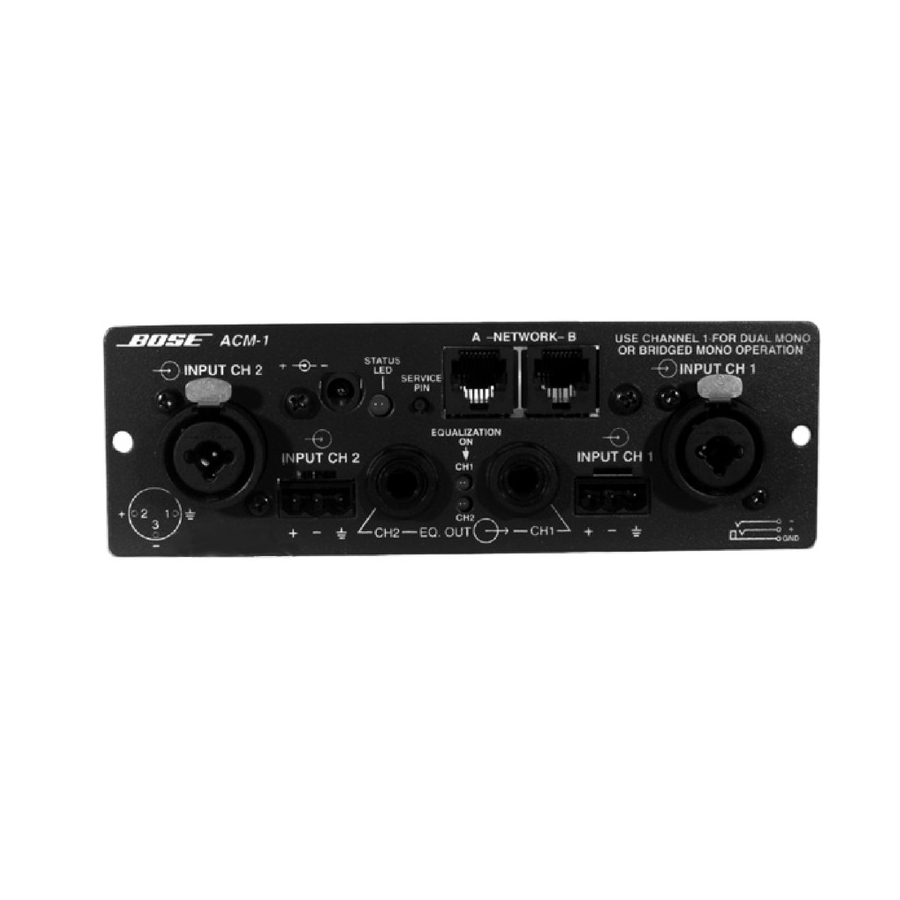
Transport or store ESDS devices in ESD protective bags, bins, or totes. Do not insert unprotected devices into materials such as plastic, polystyrene foam, clear plastic bags, bubble wrap, or plastic trays. WARRANTY INFORMATION • The ACM-1 Amplifier Control Module is covered by a 5-year transferable limited warranty. - Page 6 Power-up Gnd. I Out 1+ Sense Amplifier Rectification Mean I1_Mean I Out 1- Data Divider Activity Current Network Power I Out 2+ Sense Rectification Mean I2_Mean I Out 2- Divider Network (LonWorks ® Figure 2. ACM-1 Monitoring Section Block Diagram...
-
Page 7: Theory Of Operation
Bose PS71. See Table 2 on page 12 for part numbers for the various models. The keep-alive voltage input circuitry of the ACM-1 is designed to also allow the use of a DC external stand-by power source. The nominal power requirements for a DC source are +12 Vdc at 100 mA. - Page 8 THEORY OF OPERATION Power Supply Section: The required keep-alive voltage for the ACM-1 enters the unit at J11 [C7] as V_IN. This input voltage is rectified, if necessary, by D32 and C44 [C7]. The DC voltage is regulated by the +5V regulator U18 [C7]. This keep-alive power is required by the components that ®...
- Page 9 Neuron. The 3.16 k Ohms resistors R40, 41, and 42, protect U14 from damage when the ACM-1 is in standby mode. In this mode, the attenuator is off, but the Neuron is still powered. The quad-NAND U21 [Sheet 2, C4/5] generates VCLK from the ENABLE and CLOCK signal.
- Page 10 THEORY OF OPERATION The ADC inputs are all equipped with diode clamps to protect its inputs from damage due to a 15V input signal. This failure could occur if one of the components connected to the ADC fails and shorts one of the 15V rails to the inputs. The resistors on the inputs of the ADC protect the input stages of the converter against excessive currents due to fault signals.
-
Page 11: Disassembly/Assembly Procedures
DISASSEMBLY/ASSEMBLY PROCEDURES Note: In order to test the ACM-1 Amplifier Control Module, you must first remove the standard input module that is supplied by the factory from the rear of the amplifier. 1. Input Module Removal 1.1 Use a phillips-head screwdriver to remove the two screws from the input module connector panel. - Page 12 Note: The ACM-1 Module will not operate properly unless at least one screw is used to secure it to the amplifier. The faceplate of the ACM-1 is used to provide a ground connection to the amplifier. 3. ACM-1 Module Removal 3.1 Use a phillips-head screwdriver to...
-
Page 13: Test Procedures
EQ Output Ch. 2 Balanced TRS; tie LO to ring, tie HI to tip, tie ground to sleeve. Table 1. ACM-1 Input, Output, and Power Connections Test Setup Parameters LonWorks database and direct communication with nodes on the 1. - Page 14 STANDBY position, you will not be able to control the amplifier using the network. Note: If there are any EQ PCBs installed in the ACM-1 at J6 or J7, be sure to remove them before testing.
- Page 15 2. Connect the network cable to J12 or J14 of the ACM-1. 3. Plug the PS71 standby power supply into J11 of the ACM-1. Connect the power cord of the PS71 to the AC mains. 4. Make all required audio input and output connections.
- Page 16 Set the gain slider for the channel under test to -100.0 dB. 5.2 Apply a 775 mVrms, 1 kHz signal to the ACM-1 Channel 1 input at P4 (or J4). 3.2 Apply a 1 Vrms, 1 kHz signal to the Channel 1 input of the ACM-1.
- Page 17 6.2 Apply a 100 mV, 1 kHz signal to the 8.2 Terminate the ACM-1 Channel 1 audio ACM-1 Channel 1 input at P4 (or J4). input at P4 (or J4) with 50 Ohms. Measure the ACM-1 Channel 1 output at P3 across 6.3 Reference a dB meter to the amplifier...
- Page 18 10.2 Apply a 200 mVrms, 1 kHz signal to the mouse. The amplifier should power up. the ACM-1 channel 1 and 2 inputs at P4 Set the gain slider for the channel under and P1. Verify that the GUI Display for Z1 test to 0.0 dB.
-
Page 19: Test Cable Construction
1600/1800VI amplifier and operate the ACM-1 outside of the amplifier chassis. Note: Be sure to connect a ground wire from the front panel of the ACM-1 to the chassis of the amplifier. The ACM-1 will not operate without this ground wire. -
Page 20: Main And Packaging Part List, Acm-1 Amplifier Control Module (See Figure 10)
CHIP, FLASH, EXTENSOR 193965-01 PCB ASSY, DAUGHTERBOARD 196387 PANEL, FRONT 188663 SCREW, MACH, M3X0.5X5.0, PAN, XREC 183435-05 PCB ASSY, MOTHERBOARD 196343 SPACER, HEX, STEEL, 6-32X.5 196392-08 MANUAL, OWNER'S GUIDE 193962 CARTON, RSC VENDOR SUPPLIED Figure 10. ACM-1 Amplifier Control Module Exploded View... -
Page 21: Electrical Part List
ELECTRICAL PART LIST Resistors Reference Description Part Number Note Designator 100K, 0805, 1/10W, 1% 133625-1003 100K, 0805, 1/10W, 1% 133625-1003 100K, 0805, 1/10W, 1% 133625-1003 100K, 0805, 1/10W, 1% 133625-1003 100K, 0805, 1/10W, 1% 133625-1003 100K, 0805, 1/10W, 1% 133625-1003 100K, 0805, 1/10W, 1% 133625-1003 100K, 0805, 1/10W, 1%... - Page 22 ELECTRICAL PART LIST Resistors Reference Description Part Number Note Designator 47K, RES NET, 1/10W, 2%, X4 196347-4702 100K, RES NET, 1/10W, 2%, X4 196347-1003 100K, RES NET, 1/10W, 2%, X4 196347-1003 5.00K, RES NET, 1/10W, 0.1%, X8 181482-5001 5.00K, RES NET, 1/10W, 0.1%, X8 181482-5001 5.00K, RES NET, 1/10W, 0.1%, X8 181482-5001...
- Page 23 ELECTRICAL PART LIST Capacitors Reference Description Part Number Note Designator .10uF, 0805, Y5V, 25V, 80% 133624 .10uF, 0805, Y5V, 25V, 80% 133624 .10uF, 0805, Y5V, 25V, 80% 133624 .10uF, 0805, Y5V, 25V, 80% 133624 .10uF, 0805, Y5V, 25V, 80% 133624 .10uF, 0805, Y5V, 25V, 80% 133624 .10uF, 0805, Y5V, 25V, 80%...
- Page 24 ELECTRICAL PART LIST Transistors Reference Description Part Number Note Designator BPLR, P, 40V, 200mA, SOT23 148596 BPLR, N, 40V, 200mA, SOT23 146819 BPLR, N, 40V, 200mA, SOT23 146819 BPLR, N, 40V, 200mA, SOT23 146819 Integrated Circuits Reference Description Part Number Note Designator OP-AMP, QUAD, SOIC-14, NJM2059...
- Page 25 ELECTRICAL PART LIST Miscellaneous Reference Description Part Number Note Designator CONN, 10X2 ROWS, .1 GRID, MALE 196364 CONN, MOLEX, PCB MT, 196365 4 PIN CONN, HEADER, W/ SPACER, 8 PIN 196359 CONN, HEADER, BTM INSERT, 4x2 PIN GRID 196358 CONN, RTANG, 3 POS, BLK 177291-03 CONN, RTANG, 3 POS, BLK 177291-03...
- Page 26 Figure 11. Daughterboard Topside Etch Layout Diagram Figure 12. Daughterboard Internal Etch Layout Diagram Figure 13. Daughterboard Bottom Etch Layout Diagram...
-
Page 27: Integrated Circuit Pinout Diagrams
10. C +INPUT 11. V- 12. D +INPUT 13. D -INPUT 14. D OUTPUT ® Bose P/N: 186065, Device Type 74HC00 Bose P/N: 187472, Device Type NJM2059 Quad Nand Gate. Quad Op-Amp. FUNCTION PIN FUNCTION 1. SWITCH 1. A OUTPUT CONTROL 2. - Page 28 INTEGRATED CIRCUIT PINOUT DIAGRAMS Inhibit CONTROLS VDD = PIN 16 COMMONS VSS = PIN 8 OUT/IN SWITCHES VEE = PIN 7 IN/OUT INHIBIT ® Bose P/N: 196351, Device Type CD4052 2x4 in/ 1 Out Multiplexer Bose P/N: 196350, Device Type TC9412AF Volume Control...
- Page 29 INTEGRATED CIRCUIT PINOUT DIAGRAMS Bose ® P/N: 196360, Device Type ADC1038 10-Bit Analog to Digital Converter with Analog Multiplexer and Track/Hold Function.
- Page 30 SPECIFICATIONS AND FEATURES SUBJECT TO CHANGE WITHOUT NOTICE ® ® Bose Corporation The Mountain Framingham Massachusetts USA 01701 P/N: 199746 Rev. 00 3/99 FOR TECHNICAL ASSISTANCE OR PART ORDERS, CALL 1-800-367-4008...
Need help?
Do you have a question about the ACM-1 and is the answer not in the manual?
Questions and answers