Table of Contents
Advertisement
Quick Links
PGA26E19BA-SWEVB008
Half Bridge Evaluation Board consisting:
1. PGA26E19BA 600V 190mΩ X-GaN Power Transistor
2. AN34092B Single channel X-GaN Gate Driver IC
3. General Purpose Half Bridge Isolator
The products and product specifications described in
the document are subject to change without notice for modification
The products and product specifications described in the
and/or improvement. At the final stage of your design, purchasing,
document are subject to change without notice for modification
or use of the products, therefore, ask for the most up-to-date
and/or improvement. At the final stage of your design,
Product Standards in advance to make sure that the latest
purchasing, or use of the products, please request for the up-to-
specifications satisfy your requirements.
date Product Standards in advance to ensure that the latest
As of March, 2017
specifications meet your requirements.
PGA26E19BA-SWEVB008 Ver. 1.1
Panasonic Industrial Devices
Sales Company of America
Panasonic Semiconductor Solutions Co. Ltd.
Two Riverfront Plaza, 7th Floor
1 Kotari-yakemachi, Nagaokakyo, Kyoto 617-8520, Japan
Newark, NJ, 07102, United States
http://www.semicon.panasonic.co.jp/en/
800-344-2112
industrial@us.panasonic.com
na.industrial.panasonic.com
Panasonic
Semiconductor Solutions Co., Ltd.
1 Kotari-yakemachi, Nagaokakyo,
Kyoto 617-8520, Japan
Tel. +81-75-951-8151
http://www.semicon.panasonic.co.jp/en
Advertisement
Table of Contents

Related Manuals for Panasonic PGA26E19BA-SWEVB008


Summary of Contents for Panasonic PGA26E19BA-SWEVB008
- Page 1 Semiconductor Solutions Co., Ltd. the document are subject to change without notice for modification The products and product specifications described in the Panasonic Semiconductor Solutions Co. Ltd. and/or improvement. At the final stage of your design, purchasing, Two Riverfront Plaza, 7th Floor...
-
Page 2: Table Of Contents
Measurement Procedures ..........................15 Low Side dV/dT test ............................18 High Side dV/dT test ............................20 Low Side Switching Loss test ........................... 22 Efficiency test ..............................24 Thermal Profile ..............................25 Thermal Cooling ............................... 26 Important Notice ............................. 27 PGA26E19BA-SWEVB008 Ver. 1.1... -
Page 3: Features
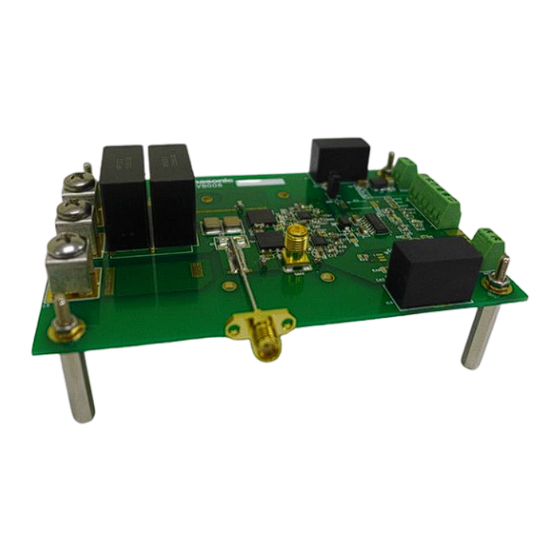
█ Facilitate gate drive design with high precision gate current source High side Iso DCDC Power AUXH+ AUXH- IN_H TPVO IN_L Shunt Resistor TPS1 TPS2 AUXL- SMA2 Semi Rigid Connector AUXL+ Low side Iso DCDC Power Figure 1A: PGA26E19BA-SWEVB008 Board Photo PGA26E19BA-SWEVB008 Ver. 1.1... -
Page 4: Description Of The Evaluation Board
PGA26E19BA-SWEVB008 Figure 1A is a complete Half bridge power circuit featuring Panasonic High Efficiency 600V 190mΩ X-GaN transistor in 8X8 SMD package and Panasonic own X-GaN driver AN34092B. The SWEVB008 provides the flexibility to be configured easily to Buck, Boost, Half bridge and Full bridge power circuit topology. -
Page 5: Recommended Operating Conditions
External clock frequency (Duty Cycle) 100kHz (pulse generator input) Continuous Pulse Tests External inductor 100uH-360uH @ DC Current>18A Room Temperature 25ºC ①②③ Power supply equipment number as illustrated in page 18, 20 and 22 Using attached heatsink PGA26E19BA-SWEVB008 Ver. 1.1... -
Page 6: Schematic Diagram
Schematic Diagram Refer to Figure 2 and 3 below for the circuit schematic of the evaluation board. Not populated Figure 2: SWEVB008 Schematic PGA26E19BA-SWEVB008 Ver. 1.1... -
Page 7: Schematic Diagram Of Optional Parts
- Schematic Diagram of optional parts Figure 3: Schematic for optional isolated DCDC power supply and Optoisolator PGA26E19BA-SWEVB008 Ver. 1.1... -
Page 8: Bill Of Materials
SMD2012 CA6,CB6 4.7uF/16V GRM21BR71C475KA73L Murata SMD2012 CA7,CB7 1uF/50V GRM21BR71H105KA12 Murata SMD2012 CA8,CB8 4.7uF/25V GRM21BR71E475KA73L Murata SMD1608 CA9,CB9 100pF/50V GRM1885C1H101JA01D SMD1608 CA10,CB10 N.M. Murata SMD3216 CA11,CB11 10uF/25V GRM31CR71E106KA12L Murata SMD1608 CA12,CB12 47pF/50V GRM1885C1H470JA01D Murata SMD3225 CA14,CB14 22uF/25V GRM32ER61E226KE15 PGA26E19BA-SWEVB008 Ver. 1.1... - Page 9 Parts Symbol Specification Part Number Manufacturer Package 51kΩ Panasonic SMD1608 ERJ-3GEYJ513V Chip Resistor 0Ω Panasonic SMD1608 ERJ-3GEY0R00V SMD1608 Chip Capacitor 100pF/50V GRM1885C1H101JA01D Murata Inverter Single inverter SN74LVC1G04 SOT-23 1 Input Half Isolator bridge Si8274GB SiLab SOIC-16 iso/driver PGA26E19BA-SWEVB008 Ver. 1.1...
-
Page 10: Pcb Layout
PCB Layout PCB Specifications: Double-sided Size: 82mm × 122mm Copper thickness: 70um Board thickness: 1.6mm Figure 4: Top and Bottom PCB Layout PGA26E19BA-SWEVB008 Ver. 1.1... -
Page 11: Test Circuits
When the inductor L1 is connected between LX and VS, buck configuration is formed (also refer as high side test). Please note that the output connection of the dead time circuit is changed accordingly so the high side GaN transistor QB acts as active power switch in buck mode. PGA26E19BA-SWEVB008 Ver. 1.1... -
Page 12: Switching Loss Test Circuit
R1. XOR1 and XOR4 logic gate produce compliment of the input signal. XOR2 and XOR3 logic gate output the signals with the delay time. The delay times can be set by adjusting the passive components R2 and R3. PGA26E19BA-SWEVB008 Ver. 1.1... -
Page 13: Efficiency Test Circuit
Figure 9 Circuit for efficiency test with high side circuit powered by bootstrap diode circuit. Figure 10 Circuit for efficiency test with high side circuit powered by isolated DCDC. PGA26E19BA-SWEVB008 Ver. 1.1... -
Page 14: Equipment
5 Power meter 3 channel power meter Yokogawa WT500 6 Electronic Load 450V/4.5kW Chroma 63804 7 Oscilloscope Tektronix DPO7104C TCP0030 Current Probe (IL) P6139B Voltage Probe ( 8 Probe P5205A Differential Voltage Probe ( BNC to SMA Cable ( PGA26E19BA-SWEVB008 Ver. 1.1... -
Page 15: Measurement Procedures
Observation of waveform will be easier if the trigger is applied at the rising / falling edge of V or V shown on Figure 13 above. If different inductor value is used other than the suggested, please set the pulse width until the desired IL value is achieved. PGA26E19BA-SWEVB008 Ver. 1.1... - Page 16 Turn On 400V 360V T-on T-off Figure 14: Measurement points for Low side device dV/dT measurement during High side device (QB) testing Turn On Turn Off 400V 360V T-on T-off Figure 15: Measurement points for High side device PGA26E19BA-SWEVB008 Ver. 1.1...
- Page 17 Set the DC power ① slowly to 0V and then follow by the DC power ② and ③ to 0V. Turn off the power. Check the V waveform and ensure that the capacitor between VPN and VS terminals has fully discharged. There is risk of electric shock due to the residual charge. PGA26E19BA-SWEVB008 Ver. 1.1...
-
Page 18: Low Side Dv/Dt Test
N5752A DC POWER ① DC power ②③ AUXH+ AUXH- 320uH Dead Time Inductor Circuit IN_L AUXL- AUXL+ 33250A SMA to probe Adapter Figure 17: Connection for Low Side GaN testing Figure 18: Evaluation Schematic for Low side GaN test PGA26E19BA-SWEVB008 Ver. 1.1... - Page 19 AUXH AUXL Important Note: The data presented is meant to demonstrate the high switching capability of Panasonic X-GaN. The dV/dT data is for reference use only and measured data maybe different depending on evaluation environment. Low side device (QA) dV/dt Measurement Data...
-
Page 20: High Side Dv/Dt Test
Figure 23 shows all the necessary connections for High Side GaN device (QB) dV/dT testing. Figure 24 shows the evaluation test circuit. Please refer to pages 15-16 for evaluation procedures. Figure 23: Connection for High side GaN test Figure 24: Evaluation schematic for High side GaN test PGA26E19BA-SWEVB008 Ver. 1.1... - Page 21 AUXH AUXL Important Note: The data presented is meant to demonstrate the high switching capability of Panasonic X-GaN. The dV/dT data is for reference use only and measured data maybe different depending on evaluation environment. High side device (QB) dV/dt Measurement Data...
-
Page 22: Low Side Switching Loss Test
Figure 29 shows all the necessary connections for Low Side GaN device (QA) Switching Loss testing. Figure 30 shows the evaluation test circuit. Please refer to page 17 for details and evaluation procedures. Figure 29: Connection for Low side switching loss test Figure 30: Test Circuit for Low side GaN switching lost test PGA26E19BA-SWEVB008 Ver. 1.1... - Page 23 AUXH AUXL Important Note: The data presented is meant to demonstrate the high switching capability of Panasonic X-GaN. The dV/dT data is for reference use only and measured data maybe different depending on evaluation environment. Low side device (QA) Switching loss Measurement Data...
-
Page 24: Efficiency Test
Efficiency test To test the efficiency of Panasonic GaN-Tr in hard switching operation, SWEVB008 board is connected in synchronous boost configuration. The input frequency for this test is 100kHz. Figure 35: Evaluation schematic for Boost DCDC Efficiency Evaluation Test Conditions: =12V, RA1,RB1=33Ω, RA2,RB2=0Ω, RA3,RB3=1Ω, CA3,CB3=330pF... -
Page 25: Thermal Profile
The thermal profile is captured during DCDC Synchronous boost test with the following test conditions: =12V, RA1,RB1 =33Ω, RA2,RB2=0Ω, RA3,RB3=1Ω, CA3,CB3=330pF AUXH AUXL VIN=200V, VOUT=394V@450W Frequency=100kHz, Inductor=200uH, Duty=50%, Dead Time=100ns Cooling Method: Natural convection, Ta = 25°C Figure 37: Thermal Profile of SWEVB008 in DCDC boost at 450W output power PGA26E19BA-SWEVB008 Ver. 1.1... -
Page 26: Thermal Cooling
Adhesive Thermal Tape: T GLOBAL Li-98 Thermal conductivity: 0.95 W/mK Conductive material: Acrylic, Fibreglass Thermal impedance: 1.8°C/W Breakdown voltage : > 3,000 Vac Operating temperature: -30 ~ 120°C Heat Sink: Fischer Elektronik ICK SMD E15 Figure 38: Mounted Heatsink information and picture PGA26E19BA-SWEVB008 Ver. 1.1... -
Page 27: Important Notice
The user assumes all responsibility and liability for proper and safe handling of this evaluation board. Further, the user indemnifies Panasonic from all claims arising from the handling or use of the evaluation boards. The technical information described in this document is intended only to show the main characteristics and application circuit examples of the products. - Page 28 PGA26E19BA-SWEVB008 Ver. 1.1...
Need help?
Do you have a question about the PGA26E19BA-SWEVB008 and is the answer not in the manual?
Questions and answers