Table of Contents
Advertisement
Quick Links
Advertisement
Table of Contents
Troubleshooting

Subscribe to Our Youtube Channel
Related Manuals for Boonton 8210-01-S/3


Summary of Contents for Boonton 8210-01-S/3
- Page 3 INSTRUCTION MANUAL MODEL 8210-01-S/3 F.M.-A.M. MODULATION METER N 0 0 1 0 4 - 8 8 - D - D 0 5 8 N00104-91-D-M090 7Z 6625-01-284-8256 BOONTON ELECTRONICS CORPORATION 791 ROUTE 10 - RANDOLPH, NJ 07869-1980 PHONE: (201)584-1077 FAX: (201)584-3037 Part No.
- Page 4 Failure to comply with these precautions or with specific warnings elsewhere in this manual violates safety standards of design, manufacture, and intended use of the instrument. Boonton Electronics assumes no Iiability for the customer's failure to comply with these requirements.
- Page 5 BOONTON ELECTRONICS CORPORATION 8210-01-S/3 Instruction-Manual SUPPLEMENT: MODEL as required to correct errors Instruction -manual supplements issued in a manual, and to adapt the manual to changes made after its printing. Para. 1-2. b. Page 1-1, replace "Each time it is turned on, . . ."with "When the LEVEL key is depressed at power on, .
- Page 6 Page 3-13, Para. 3-3 e add sub-paragraph (8) “Non-volatile operation of A4U13 is controlled byU31. This circuit switches the Vcc connection of A4U13 from the + 5L supply to the battery supply, BT1 and BT2, when the + 5L supply falls below the battery voltage. Additionally, U31 inhibits the chip enable signal at pin 18 of A4U13 when the + 5L supply drops below 4.75 volts.
- Page 7 Page 6-9,10, Figure 6-5 modify schematic as follows: Page 6-13,14 Figure 6-7 modify schematic as follows: change voltage at C26 from 8.7V to 9.7V change voltage at C27 from 20V to 22V change voltage at C25 from -20V to -22V...
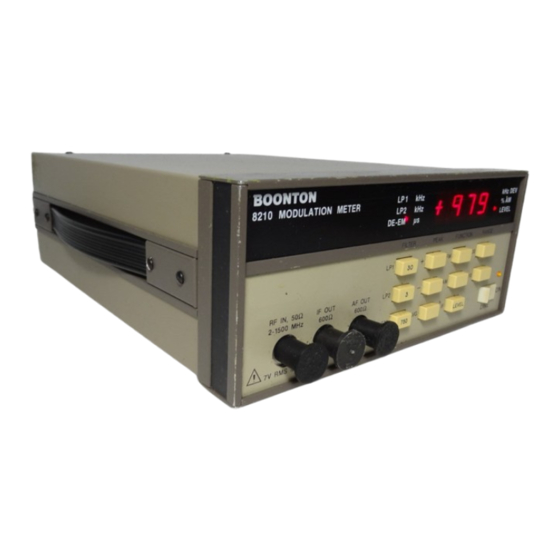
- Page 8 Figure 1-1. Model 8210 F.M.-A.M. Modulation Meter 8210-1182...
-
Page 9: Table Of Contents
T A B L E C O N T E N T S SECTION I - INTRODUCTION PAGE SUBSECTION Safety Notice ..........Description of the Instrument . - Page 10 AND ADJUSTMENT SECTION IV - MAINTENANCE PAGE SUBSECTION Introduction ... . Test Equipment Required. Location of Major Assemblies Removal of Major Assemblies and Parts a. Instrument Covers. . . R.F .-Assembly Cover. c.
- Page 11 LIST OF ILLUSTRATIONS (CONTINUED) PAGE FIGURE 2-11 Test Setup: Residual F.M., Residual A.M....Test Setup: A.M. Rejection, Frequency Response, Audio Distortion. 2-12 Test Setup: F.M. Audio Distortion, F.M. Rejection ..2-13 Packaging Diagram .
-
Page 13: Safety Notice
1-2. DESCRIPTION The Model 8210 Modulation Meter, manufactured by Boonton Electronics Corp., instrument that measures and displays the de- is a versatile, solid-state viation of frequency-modulated signals or the percentage modulation of amplitude-modulated signals over a carrier range of 2 MHz to 1.5 GHz. -
Page 14: Items Furnished
ITEMS FURNISHED 1-3. For making measure- The instrument is supplied complete with power cord. ments the connection of various cables will be called for, depending upon Required cable connections are discussed the operating mode of the 8210. in paragraph 2.1d. 1-4. - Page 15 S1-6, Continued. AMPLITUDE MODULATION 10% and 100%, full scale Modulation-Depth Ranges Modulation Accuracy Depth Accuracy 10% to 90% A.M. Frequency 50 Hz to 5 kHz 1% of reading 3% of reading 6% of reading 2% of reading kHz to 7.5 kHz NOTE: Peak residuals must be accounted for to obtain the above accuracies.
- Page 16 S1-6, Continued. 103 mm high x 218 wide x 278 deep DIMENSIONS (4.1 in. x 8.6 x 11.0) 3.18 kg (7.0 lbs.), approximately. WEIGHT OPTIONAL MODEL 8210-01 This model is the same as the standard Model 8210 except as follows: AUDIO-FREQUENCY RESPONSE The 15 kHz low-pass filter is replaced by Filters...
-
Page 17: Installation
S E C T I O N INSTALLATION & OPERATION 2-1. INSTALLATION The 8210 is shipped complete and ready for use. Unpack the Unpacking. equipment from the shipping container and inspect it for any damage that may have occured during shipment. Check that all connectors and switches operate without binding. -
Page 18: Operating Controls, Indicators And Connectors
2-2. OPERATING CONTROLS, INDICATORS AND CONNECTORS All controls, indicators and connectors used during operation of the 8210 They are described in Table are shown in Figures 2-1 and 2-2. 2-1, below. operating Controls, Indicators, and Connectors Table 2-1. 8210-1182... - Page 19 Figure 2-1. Model 8210, Front View Figure 2-2. Model 8210, Rear View 8210-1182...
-
Page 20: Preliminary Check
2-3. PRELIMINARY CHECK NOTE: The following preliminary check procedure is intended only to ensure If a detailed performance check against that all circuits are operating. specifications is desired, refer to subsection 2-6. Before using the Model 8210, perform a preliminary check as follows: The LED display should in- Set the LINE switch to the “on”... - Page 21 Figure 2-3. Residual P. M., Typical Figure 2-4. Residual Typical A. M., 8210-1182...
- Page 22 Figure 2-5. Audio Response, Typical 8210-1182...
- Page 23 Additional Applications. Information relevant to further applications of the 8210 will be found in Boonton Electronics’ Application Note $19: High Accuracy AM-FM Measurements with the Boonton 82AD Modulation Meter. The Application Note is available free upon request to Boonton Electronics.
-
Page 24: Operating Instructions
2-5. OPERATING INSTRUCTIONS The operation is essentially automatic, requiring only of The Model 8210 that the operator select the proper display function and baseband filter. Paragraphs 2-5a and 2-5b summarize operating steps for a.m. and f.m. meas- urements, respectively. A.M. Measurements. Set the LINE switch to ON, and connect to the RF IN connector the r.f. -
Page 25: Test Equipment Required
2-6. PERFORMANCE VERIFICATION tests may be performed when the Model 8200 is first received. The following Thereafter, performance verification should be needed only after repair to the instrument. some settings or results are In these verification procedures, NOTE: These parenthetical entries followed by data in parentheses. - Page 26 S2-6, Continued. b. R.F. Input Sensitivity. Connect the 8210 and test equipment as shown in Figure 2-6. Depress the switches of the 8210 as indicated in Figure 2-6. 10 mV r.m.s. signal from the Model 102E-19 signal Apply a 10 MHz, The 8210 should in- generator to the...
- Page 27 S2-6, Continued. Residual F.M. Connect the 8210 and test equipment as shown in Figure 2-7. at 0 dBm, from the test source to the RF Apply the 500 signal, IN connector of the 8210. Depress the switches of the 8210 as indicated in Figure 2-7. (without 600 Q termination) to the AF Connect the r.m.s.
- Page 28 S2-6, Continued. f. A.M. Rejection. (1) Connect the 8210 and test equipment as shown in Figure 2-8. Set the 8210’s controls as shown in Figure 2-8. Apply a 30 MHz signal, at 0 dBm, from the generator to the mixer. Adjust the Adjust the power-supply output voltage to +10 V d.c.
- Page 29 S2-6h, Continued. to 7.5 kHz (15 kHz). The indicated a.m. (5) Increase the frequency and 61.2%. should be between 58.8% to 15.0 (30 kHz). The indicated a.m. the frequency (6) Increase and 44.38. should be between 40.4% F.M. Audio Distortion. (1) Connect the 8210 and test equipment as shown in Figure 2-9.
-
Page 30: Packaging Diagram
S2-6, Continued. Audio-Frequency Response, 3 kHz. Connect the equipment as in 2-9. Figure Set the 8210’s controls as shown. Adjust the audio oscillator’s frequency to 300 Hz, then adjust its amplitude until the 8210 reads 100.0 kHz. Without changing adjust its the audio oscillator’s level, frequency to exactly 3.00 kHz. -
Page 31: Simplified Block Diagram
S E C T I O N I I I THEORY OF OPERATION 3-1. 1NTRODUCTION The 8210 is a compact, microprocessor-controlled, internally calibrated, a.m.-f.m. modulation meter that covers the carrier-frequency range of 2 MHz to 1.5 GHz. Amplitude modulation frequency modulation is displayed on a four-digit display that provides a maximum resolution of 0.01% a.m. - Page 32 3-2a, Continued. A sampling pulse, generated from a tunable local oscillator, converts the The if. signal r.f. signal into an if. signal at approximately 400 kHz. is passed to the if. circuits and also through a filter to a limiter, a Automatic frequency control is ac- discriminator, and an error amplifier.
-
Page 33: Circuits: Detailed Block Diagram
Figure 3-2. Block R.F. Circuits: Detailed Diagram 8210-1182... -
Page 34: Sampling Gate: Simplified Operation
3-3a(l), Continued. through Q6 and associated components, constitute a zero-order hold sampler. (2) The operation of the sampling gate is shown in simplified form in Each time the sampling gate is closed, by a short- Figure 3-3. duration pulse, the input capacitance of the sampler amplifier plus any stray capacitance is charged to a voltage that is less than the Before the next sample is taken, instantaneous r.f. - Page 35 Continued. 3-3a(5), frequency changes from less than 30 approximately 40 MHz. MHz to Level shifter Q7 increases the signal to TTL-compatible levels to drive both U2 and U3d (a buffer), and U1b (a divide-by-two stage). able to divide by U3a-c are configured as a programmable counter, four, by five, or by six, as controlled by the logic circuitry.
-
Page 36: I.f. Circuits: Detailed Block Diagram
I.F. Circuits: Detailed Block Diagram Figure 3-4. 8210-1182... - Page 37 3-3b(1), Continued. connected The signal is then to calibrator switch R3, R5, R6 & R8. The gain of the determined DAC is U3, and a.c. -coupled to DAC U4. The logic circuitry by the digital byte appearing at inputs B1-B8. varies this byte in order to maintain the d.c.
-
Page 38: Calibrator Circuits: Detailed Block Diagram
Calibrator Circuits: Detailed Block Figure 3-5. Diagram 8210-1182... -
Page 39: A.f. Circuits: Detailed Block Diagram
Figure 3-6. A.F. Circuits: Detailed Block Diagram 8 2 1 0 - 1 1 8 2... - Page 40 Continued 3-3C(2), circuits. This signal is amplified (x2) by A3U1 and applied to the voltage divider A3R7. The analog switch A3U3 is controlled by the 874-Hz signal from A4U12 so as to switch between two taps of the divider. The voltage ratio is exactly two, therefore the equivalent a.m.
-
Page 41: Logic Circuits: Detailed Block Diagram
Logic Circuits: Detailed Figure 3-7. Block Diagram 3-11 8210-0184... -
Page 42: Program Flow Diagram
3-3e, Continued. by the PIA U17. See Figures 3-7 and 3-8. and display functions are directed The control program initializes the RAM and PIA circuits and checks the status of the test switch during the power-up sequence. processing of the keyboard display is then enabled, and interrupt As each digit of the display is updated,... - Page 43 3-3e(4), Continued. connected to it, as are the outputs of the integrator and the dis- circuits, and the d.c. level from the a.m. criminator from the r.f. The a.m. detector output is filtered by R21 and C56 to detector. and C15 to provide another. provide one a.m.-level input and by R20 The two a.m.
- Page 44 3-3f(4), Continued. developed by the resistive divider composed of R31d and R31f, is compared to ground. Error voltages are amplified by U29b, and are coupled to regulator U28 in order to adjust the output voltage so as to reduce the error. In this manner the -15 volt supply is made to track the +15 volt supply.
-
Page 45: Location Of Major Assemblies
S E C T I O N MAINTENANCE AND ADJUSTMENT 4-1. INTRODUCTION and adjustment instructions for the Model This section contains maintenance and systematic troubleshooting procedures for localizing 8210. Symptomatic a malfunction are given, as well. 4-2. TEST EQUIPMENT REQUIRED The test equipment that is required for maintenance and of the adjustment... -
Page 46: Model 8210: Top View With Covers Removed
Digital/Power Supply PCB (A4) Model 8210: Top View with Covers Removed Figure 4-1. 8210-1182... -
Page 47: Model 8210: Bottom View With Covers Removed
Figure 4-2. Model 8210: Bottom View with Covers Removed 8210-1182... -
Page 48: Assembly Cover
4-4a, Continued. Remove the cover by lifting up and toward the rear of the unit. Turn the instrument over and remove the two #4-40 screws securing bottom cover. Remove the bottom cover as in Step (3). R.F.-Assembly Cover. the 8210’s covers as in 4-4a. Remove Place instrument... -
Page 49: Digital Circuits And Power-Supply Board
4-4e, Continued. (4) Remove three #6-32 screws securing the rear panel to the chassis. (5) Remove two 44-40 screws securing the rear panel to the power-supply heat sink. Pull the rear panel away from the chassis. Digital Circuits and Power-Supply Board. Remove the instrument’s covers (14-4a). -
Page 50: Preliminary Checks
S4-5, Continued. Standard printed-circuit-board maintenance techniques are required for the Excessive heat must be avoided; a low- removal and replacement of parts. together with suitable heat sinks, should be used wattage soldering iron, for all soldering and unsoldering operations. 4-6. PRELIMINARY CHECKS check If equipment malfunction occurs, perform a visual... -
Page 51: Troubleshooting
4-7. TROUBLESHOOTING Concepts. Logical trouble-localization involves three major procedures: symptomatic troubleshooting, used to localize the cause of a mal- function to a major circuit group; systematic troubleshooting within the affected circuit group, used to localize the cause to a specific circuit or stage; and, voltage measurements, waveform analysis, or signature analysis--all used to isolate the defective part. -
Page 52: Condition-Code Displays
Table 4-3. Condition-Code Displays Table 4-4. Troubleshooting Test-Switch Chart 8210-1182... -
Page 53: Symptomatic Troubleshooting Chart
Troubleshooting Test-Switch Chart (Continued) Table 4-4. Table 4-5. Symptomatic Troubleshooting Chart 8210-0184... -
Page 54: Systematic Troubleshooting Chart: R.f. Circuits
Table 4-5. Symptomatic Troubleshooting Chart (Continued) Table 4-6. Systematic Troubleshooting Chart: R.F. Circuits 4-10 8210-1182... -
Page 55: Systematic Troubleshooting Chart
Systematic Troubleshooting Chart: R.F. Circuits (Continued) Table 4-6. 8210-1182 4-11... -
Page 56: Systematic Troubleshooting
Table 4-6. Systematic Troubleshooting Chart: R.F. Circuits (Continued) 4-12 8210-1182... -
Page 57: Systematic Troubleshooting Chart
Systematic Troubleshooting Chart: R.F. Circuits (Continued) Table 4-6. 8210-1182 4-13... -
Page 58: Systematic Troubleshooting Chart: I.f. Circuits
Table 4-7. Systematic Troubleshooting Chart: I.F. Circuits 8210-1182 4-14... - Page 59 Table 4-7. Systematic Troubleshooting Chart: I.F. Circuit (Continued) 8210-1182 4-15...
-
Page 60: Systematic Troubleshooting Chart: A.f. Circuits
Systematic Troubleshooting Chart: I.F. Circuits (Continued) Table 4-7. Table 4-8. Systematic Troubleshooting Chart: A.F. Circuits 8210-1182 4-16... - Page 61 Table 4-8. Systematic Troubleshooting Chart: A.F. Circuits (Continued) 8210-1182 4-17...
- Page 62 Table 4-8. Systematic Troubleshooting Chart: A.F. Circuits (ContinueD) 4-18 8210-1182...
- Page 63 Table 4-8. Systematic Troubleshooting Chart: A.F. Circuits (Continued) 8210-1182 4-19...
- Page 64 Table 4-9. Systematic Troubleshooting Chart: Logic Circuits 4-20 8210-0184...
- Page 65 Table 4-9. Systematic Troubleshooting Chart: Logic Circuits (Continued) 8210-1182 4-21...
- Page 66 Systematic Troubleshooting Chart: Logic Circuits (Continued) Table 4-9. 8210-1182 4-22...
- Page 67 Systematic Troubleshooting Chart: Logic Circuite (Continued) Table 4-9. Table 4-9a. Signature-Analysis Chart: Address Field 8210-0184 4-23...
- Page 68 Signature-Analysis Chart: Decoder Circuit Table 4-9b. Table 4-9c. Signature-Analysis Chart: PROM A4U11 (June, 1983)* 4-24 8210-0184...
- Page 69 Systematic Troubleshooting Chart: Calibrator Circuits Table 4-10. 8210-1182 4-25...
-
Page 70: Adjustment And Alignment Procedures
Systematic Troubleshooting Chart: Power Supply Table 4-11. 4-8. ADJUSTMENT AND ALIGNMENT PROCEDURES This subsection lists all required adjustments and alignment Procedures. Note, however, that adjustment is not a substitute for troubleshooting: be certain that all other possible causes of equipment malfunction have been eliminated before making adjustments. -
Page 71: Test Setup: Adjustment And Alignment
Continued. 4-8, Test Setup: Adjustment and Alignment Figure 4-3. Efficiency and F.M. Rejection. R.F. Replace the r.f.-assembly cover. Set the oscilloscope to 0.05 V/division and 1 ins/division. Apply 100 kHz deviation Set the signal generator to 2 dBm. MHz, 0 settle to within f 5 kHz of at a 1 kHz rate. - Page 72 Systematic Troubleshooting: Waveforms Table 4-12. 8210-1182 4-20...
- Page 73 Table 4-12. Systematic Troubleshooting: Waveforms (Continued) 8210-1182 4-29...
- Page 74 Systematic Troubleshooting Waveforms (Continued) Table 4-12. 8210-1182 4-30...
- Page 75 Troubleshooting: Waveforms (Continued) Table 4-12. Systematic 8210-1182 4-31...
- Page 76 Systematic Troubleshooting: Waveforms (Continued) Table 4-12. 4-32 8210-1182...
- Page 77 Systematic Troubleshooting: Waveforms (Continued) Table 4-12. 8210-1182 4-33...
-
Page 79: Introduction
S E C T I O N REPLACEABLE PARTS INTRODUCTION 5-1. Parts, identifies the manufacturers of components by Table 5-2, Replaceable five-digit groups taken from the Federal Supply Code for Manufacturers. A list of the applicable code groups and manufacturers is given in Table 5-1. The Table of Replaceable Parts begins with major assemblies, including PC followed by miscellaneous parts and boards complete with all their parts,... - Page 80 Table 5-2. Replaceable Parts 5 - 2 5210-1188...
- Page 81 Table 5-2. Replaceable Parts (Continued) 8210-1188 5 - 3...
- Page 82 Table 5-2. Replaceable Parts (Continued) 5 - 4 8210-1188...
- Page 83 Replaceable Parts (Continued) Table 5-2. 8210-1188...
- Page 84 Table 5-2. Replaceable Parts (Continued) 5 - 6 8210-1188...
- Page 85 Replaceable Parts (Continued) Table 5-2. 8210-1188...
- Page 86 Table 5-2. Replaceable Parts (Continued) 8210-1188...
- Page 87 Table 5-2. Replaceable Parts (Continued) 8210-1188...
- Page 88 Table 5-2. Replaceable Parts (Continued) 5-10 8210-1188...
- Page 89 Replaceable Parts (Continued) Table 5-2. 5-11 8210-1188...
- Page 90 T a b l e 5 - 2 . R e p l a c e a b l e P a r t s ( C o n t i n u e d ) 8210-1188 5-12...
- Page 91 S E C T I O N SCHEMATIC DIAGRAMS TABLE OF CONTENTS 6 - 1 . Page F i g u r e Main-Frame Schematic Diagram (E831193C, Sheet 1 of 4) ....6-3 6 - 1 .
- Page 92 N O T E S 8 2 1 0 - 0 1 8 4...
- Page 93 F i g u r e 6 - 2 . I . F . - A . F . B o a r d S c h e m a t i c ( E 8 3 1 1 9 3 C , S h e e t 6 - 3 &...
- Page 94 F i g u r e 6 - 3 . 1 . F . - A . F . B o a r d S c h e m a t i c ( E S 3 1 1 9 3 D , S h e e t 6 - 5 &...
- Page 95 F i g u r e 6 - 4 . R . F . B o a r d S c h e m a t i c (E831193D, Sheet &...
- Page 96 F i g u r e 6 - 5 . D i g i t a l & P o w e r - S u p p l y B o a r d Schematic (R831193F, Sheet & 6-10...
- Page 97 F i g u r e 6 - 6 . D i g i t a l & P o w e r - S u p p l y B o a r d S c h e m a t i c ( E 8 3 1 1 9 3 D , S h e e t 6-11...
- Page 98 F i g u r e 6 - 7 . D i g i t a l P o w e r - S u p p l y B o a r d & Schematic (D831193D, Sheet 6 - 1 3 &...
-
Page 99: Technical Discussion
A P P E N D I X CALIBRATOR OPERATION A-1. INTRODUCTION internal calibrators of the Model 8210 provide modulation standards for a.m. and f.m. measurements; they are activated each time the instrument is turned on. This section of the manual provides technical information con- cerning the operation and design of the calibrators. - Page 100 SA-2b(1), Continued. not critical since the a.g.c. system is used to normalize the a.m. detector output. The filtered signal is routed to the i.f.-a.f. circuit board via C11, which removes any d.c. component, and thence to the input of buffer U1. Amplifier U1 increases the level of the signal, and more importantly, provides a very low output impedance to drive the voltage divider consisting of A3R7a, b, and...
- Page 101 ¶A-2b(5), Continued. Now, since the peak detectors are a.c. coupled, (0 volts, d.c.) (p+)(T ) - (p_ (T ) = 0 And: (p+) (T ) - (p_)(1 - T ) = 0 Now: ( 1 0 ) a v g m i n And, in the 8210: (11)
- Page 102 Actual noise levels are less than 1 part in 3333. (8) Cross-correlation measurements using a specially calibrated Model 82AD F.M.-A.M. Modulation Meter (Boonton electronics) indicate that the actual calibration uncertainty for 100 calibrations is approxi- mately ± 0.15%. Audio Processing.
Need help?
Do you have a question about the 8210-01-S/3 and is the answer not in the manual?
Questions and answers