Table of Contents
Advertisement
Quick Links
Advertisement
Table of Contents

Subscribe to Our Youtube Channel
Related Manuals for Clevo W340EU


Summary of Contents for Clevo W340EU
- Page 1 W340EU/W345EU...
-
Page 3: Table Of Contents
Introduction ..........1-1 Top (W340EU) ................A-3 Bottom (W340EU) ................. A-4 Overview ..................1-1 SATA BLU RAY COMBO (W340EU) ........A-5 Specifications ..................1-2 Super Multi (W340EU) ..............A-6 External Locator - Top View with LCD Panel Open ......1-4 LCD (W340EU) ................A-7 External Locator - Front &... - Page 4 Preface PCH 7/9- PWR ................B-20 PCH 8/9 POWER ................. B-21 PCH 9/9- GRD ................B-22 USB3.0, Power, WLAN ............... B-23 CCD, 3G, TPM ................B-24 Card Reader / LAN RTL8411 ............B-25 LAN, SATA HDD, ODD ............. B-26 USB3.0 TI TUSB7320 ..............B-27 KBC-ITE IT8518 .................
- Page 5 Preface Notebook Computer W340EU/W345EU Service Manual...
- Page 6 Preface Notice The company reserves the right to revise this publication or to change its contents without notice. Information contained herein is for reference only and does not constitute a commitment on the part of the manufacturer or any subsequent ven- dor.
- Page 7 This manual is intended for service personnel who have completed sufficient training to undertake the maintenance and inspection of personal computers. It is organized to allow you to look up basic information for servicing and/or upgrading components of the W340EU/ W345EU series notebook PC.
- Page 8 Preface IMPORTANT SAFETY INSTRUCTIONS Follow basic safety precautions, including those listed below, to reduce the risk of fire, electric shock and injury to per- sons when using any electrical equipment: 1. Do not use this product near water, for example near a bath tub, wash bowl, kitchen sink or laundry tub, in a wet basement or near a swimming pool.
- Page 9 Preface Instructions for Care and Operation The notebook computer is quite rugged, but it can be damaged. To prevent this, follow these suggestions: Don’t drop it, or expose it to shock. If the computer falls, the case and the components could be damaged. Do not expose the computer Do not place it on an unstable Do not place anything heavy...
- Page 10 Preface Avoid interference. Keep the computer away from high capacity transformers, electric motors, and other strong mag- netic fields. These can hinder proper performance and damage your data. Take care when using peripheral devices. Use only approved brands of Unplug the power cord before peripherals.
- Page 11 Preface Battery Precautions • Only use batteries designed for this computer. The wrong battery type may explode, leak or damage the computer. • Do not continue to use a battery that has been dropped, or that appears damaged (e.g. bent or twisted) in any way. Even if the computer continues to work with a damaged battery in place, it may cause circuit damage, which may possibly result in fire.
- Page 12 Preface Related Documents You may also need to consult the following manual for additional information: User’s Manual on CD/DVD This describes the notebook PC’s features and the procedures for operating the computer and its ROM-based setup pro- gram. It also describes the installation and operation of the utility programs provided with the notebook PC. System Startup 1.
-
Page 13: Introduction
Chapter 1: Introduction Overview This manual covers the information you need to service or upgrade the W340EU/W345EU series notebook computer. Information about operating the computer (e.g. getting started, and the Setup utility) is in the User’s Manual. Information about dri-vers (e.g. VGA & audio) is also found in the User’s Manual. The manual is shipped with the computer. -
Page 14: Specifications
Introduction Specifications Processor Options Core Logic Intel® Core™ i7 Processor Intel® HM76 Chipset i7-3612QM (2.1GHz) BIOS 6MB L3 Cache, 22nm, DDR3-1600MHz, TDP 35W i7-3520M (2.90GHz) One 32Mb SPI Flash ROM Latest Specification Information 4MB L3 Cache, 22nm, DDR3-1600MHz, TDP 35W AMI BIOS The specifications listed here are correct at the Intel®... - Page 15 Dimensions & Weight Combo Drive Module) (Factory Option) 300K/1.3M Pixel USB PC Camera Module One Changeable 2.5" 9.5mm (h) SATA HDD W340EU: (Factory Option) 3.75G/HSPA Mini-Card Module 342mm (w) * 241.5mm (d) * 34.95mm (h) Pointing Device WLAN/ Bluetooth Half Mini-Card Modules: 2.1 kg (with 48.84WH Battery and ODD)
-
Page 16: External Locator - Top View With Lcd Panel Open
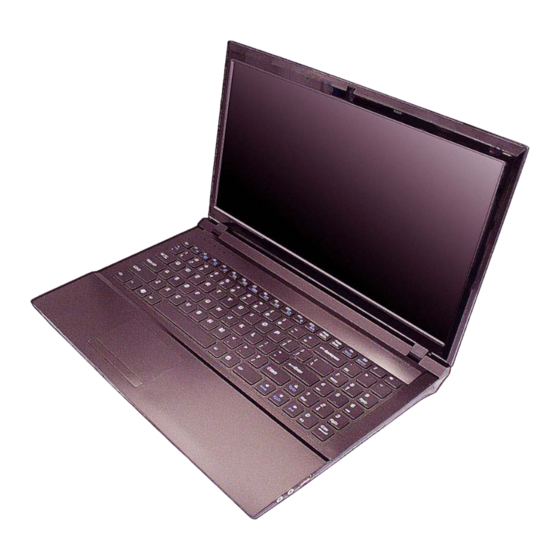
1. PC Camera (Optional) 2. Built-In Microphone 3. LCD 4. Power Button 5. Hot-Key Buttons (Model A Only) 6. Keyboard W340EU W345EU 7. Touchpad & Buttons 8. LED Status Indicators 1 - 4 External Locator - Top View with LCD Panel Open... -
Page 17: External Locator - Front & Right Side Views
Introduction External Locator - Front & Right Side Views Figure 2 Front View 1. LED Power Indicator FRONT VIEW W340EU W345EU Figure 3 Right Side View RIGHT SIDE VIEW 1. Microphone-In Jack 2. Headphone-Out Jack W340EU 3. USB 2.0 Port 4. -
Page 18: External Locator - Left Side & Rear View
External Locator - Left Side & Rear View Figure 4 Left Side View 1. DC-In Jack LEFT SIDE VIEW 2. External Monitor Port W340EU 3. RJ-45 LAN Jack 4. HDMI-Out Port 5. USB 3.0 Ports 6. Vent W345EU 7. e-SATA Port 8. -
Page 19: External Locator - Bottom View
Introduction External Locator - Bottom View Figure 6 Bottom View 1. Battery 2. Component Bay Cover 3. Vent 4. Hard Disk Bay W340EU W345EU Cover 5. Speakers Overheating To prevent your com- puter from overhea- ting, make sure no-... -
Page 20: Mainboard Overview - Top (Key Parts)
Introduction Mainboard Overview - Top (Key Parts) Figure 7 Mainboard Top Key Parts 1. KBC-ITE IT8518 2. Audio Codec ALC269 3. JMICRO JMC251 C 1 - 8 Mainboard Overview - Top (Key Parts) -
Page 21: Mainboard Overview - Bottom (Key Parts)
Introduction Mainboard Overview - Bottom (Key Parts) Figure 8 Mainboard Bottom Key Parts 1. Memory Slots DDR3 SO-DIMM 2. CPU Socket (no CPU installed) 3. CMOS Battery 4. Mini-Card Connector (WLAN Module) 5. Mini-Card Connector (3G Module) 6. nVIDIA VGA 7. -
Page 22: Mainboard Overview - Top (Connectors)
Introduction Mainboard Overview - Top (Connectors) Figure 9 Mainboard Top Connectors 1. HDMI-Out Port 2. USB Port 3.0 3. Audio Board Connector 4. TouchPad Cable Connector 5. Switch Board Cable Connector 1 - 10 Mainboard Overview - Top (Connectors) -
Page 23: Mainboard Overview - Bottom (Connectors)
Introduction Mainboard Overview - Bottom (Connectors) Figure 10 Mainboard Bottom Connectors 1. ODD Connector 2. HDD Connector 3. Cable Connector 4. Keyboard Cable Connector 5. CPU Fan Cable Connector 6. Multi-in-1 Card Reader 7. RJ-45 LAN Jack 8. External Monitor Port 9. - Page 24 Introduction 1 - 12...
-
Page 25: Disassembly
Chapter 2: Disassembly Overview This chapter provides step-by-step instructions for disassembling the W340EU/W345EU series notebook’s parts and subsystems. When it comes to reassembly, reverse the procedures (unless otherwise indicated). We suggest you completely review any procedure before you take the computer apart. -
Page 26: Maintenance Tools
Disassembly NOTE: All disassembly procedures assume that the system is turned OFF, and disconnected from any power supply (the battery is removed too). Maintenance Tools The following tools are recommended when working on the notebook PC: • M3 Philips-head screwdriver •... -
Page 27: Maintenance Precautions
Disassembly Maintenance Precautions The following precautions are a reminder. To avoid personal injury or damage to the computer while performing a re- moval and/or replacement job, take the following precautions: Power Safety Warning 1. Don't drop it. Perform your repairs and/or upgrades on a stable surface. If the computer falls, the case and other Before you undertake components could be damaged. -
Page 28: Disassembly Steps
Disassembly Disassembly Steps The following table lists the disassembly steps, and on which page to find the related information. PLEASE PERFORM THE DISASSEMBLY STEPS IN THE ORDER INDICATED. To remove the Battery: To remove the Wireless LAN Module: 1. Remove the battery page 2 - 5 1. -
Page 29: Removing The Battery
Disassembly Removing the Battery Figure 1 Battery Removal 1. Turn the computer off, and turn it over. 2. Slide the latch in the direction of the arrow (Figure 1a a. Slide the latch and hold it 3. Slide the latch in the direction of the arrow, and hold it in place (Figure 1a in place. -
Page 30: Removing And Installing The Component Bay Cover
Figure 2 Bay Cover Removal To upgrade any components you need to remove the component bay cover first. The procedure for removing the com- (W340EU) ponent bay cover will depend upon your particular computer model: a. Remove the screws. Component Bay Cover Removal Procedure b. - Page 31 Disassembly (W345EU) 1. Turn off the computer, turn it over, and remove the battery (page 2 - 2. Locate the component bay cover and remove screws (Figure 3a). Figure 3 3. Lift the cover off computer at point Bay Cover Removal 4.
- Page 32 Disassembly Component Bay Cover Installation Procedure Figure 4 Bay Cover (W340EU) Installation 1. Reinsert the component bay cover by placing it on the bottom case assembly and sliding it on to the case in the (W340EU) direction of arrow (and make sure you press down on the case at point...
- Page 33 Disassembly (W345EU) 1. This computer model has four component bay cover pins , and these need to be aligned with slots in the Figure 5 case to insure a proper cover fit (Figure 5a). Bay Cover 2. After inserting the bay cover replace the screws (Figure 5b).
-
Page 34: Removing The Hard Disk Drive
(h). Follow your operating system’s installation instructions, and install all necessary drivers and utilities (as outlined in HDD Assembly Chapter 4 of the User’s Manual) when setting up a new hard disk. Removal (W340EU) Hard Disk Upgrade Process a. Remove the screw and lift... - Page 35 7. Remove the screw and the mylar cover from the hard disk (Figure 7e W340EU - Removal ( 8. Reverse the process to install a new hard disk (do not forget to replace all the screws and covers). cont’d.) 9. Replace the hard disk bay cover by inserting it at an angle, replace the screw, and then replace the component bay cover (see page f.
- Page 36 Disassembly W345EU Figure 8 1. Turn off the computer, and remove the battery (page 2 - 5) and component bay cover (page 2 - HDD Assembly 2. Lift the hard disk bay cover up from point (Figure Removal (W345EU) 3. Remove hard disk bay cover (Figure 8b).
- Page 37 Disassembly 5. Lift the hard disk assembly out of the bay (Figure 9d Figure 9 6. Remove the screw and the mylar cover from the hard disk (Figure 9e HDD Assembly 7. Reverse the process to install a new hard disk (do not forget to replace all the screws and covers). W345EU - Removal ( 8.
-
Page 38: Removing The Optical (Cd/Dvd) Device
1. Turn off the computer, remove the battery (page 2 - 5) and component bay cover (page 2 - Removal (W340EU) 2. Remove the screw at point (Figure 10a 3. Use a screwdriver to carefully push out the optical device... - Page 39 Disassembly W345EU Figure 11 Optical Device 1. Turn off the computer, remove the battery (page 2 - 5) and component bay cover (page 2 - Removal (W345EU) 2. Remove the screw at point (Figure 11a 3. Use a screwdriver to carefully push out the optical device at point (Figure 11b a.
-
Page 40: Removing The System Memory (Ram)
Disassembly Removing the System Memory (RAM) Figure 12 RAM Module The computer has two memory sockets for 204 pin Small Outline Dual In-line Memory Modules (SO-DIMM) supporting Removal DDRIII (DDR3) Up to 1066/1333 MHz. The main memory can be expanded up to 8GB. The SO-DIMM modules sup- ported are 1024MB and 2048MB DDRIII Modules. -
Page 41: Removing And Installing A Processor
Disassembly Removing and Installing a Processor Processor Removal Procedure Figure 13 1. Turn off the computer, turn it over, and remove the battery (page 2 - 5) and the component bay cover (page 2 - Processor Removal 2. Remove screws from the CPU fan (Figure 13a). - Page 42 Disassembly 7. Turn the release latch towards the unlock symbol to release the CPU (Figure 14d). Figure 14 8. Carefully (it may be hot) lift the CPU up and out of the socket (Figure 14e). Processor Removal 9. Reverse the process to install a new CPU. (cont’d) 10.
- Page 43 Disassembly Processor Installation Procedure Figure 15 Processor 1. Insert the CPU (Figure 15a), pay careful attention to the pin alignment, it will fit only one way (DO NOT Installation FORCE IT!), and turn the release latch towards the lock symbol (Figure 15b).
-
Page 44: Removing The 3.75G Module
Disassembly Removing the 3.75G Module Figure 16 3G Module Removal 1. Turn off the computer, turn it over, and remove the battery (page 2 - 5) and the component bay cover (page 2 - 2. The 3.75G module will be visible at point on the mainboard (Figure 16a). -
Page 45: Removing The Wireless Lan Module
Disassembly Removing the Wireless LAN Module Figure 17 Wireless LAN 1. Turn off the computer, turn it over, and remove the battery (page 2 - 5) and the component bay cover (page 2 - Module Removal 2. The Wireless LAN module will be visible at point on the mainboard (Figure 17a). -
Page 46: Removing The Ccd
Disassembly Removing the CCD Figure 18 CCD Removal 1. Turn off the computer, turn it over and remove the battery (page 2 - 2. Open the LCD and carefully remove the rubber screw covers & and set them aside (Figure 18a) and a. - Page 47 Disassembly 5. Disconnect the cable from the module. Figure 19 6. Remove the CCD module (Figure 19e). CCD Removal (cont’d) d. Disconnect cable. e. Remove the CCD mo- dule. 12. CCD Module Removing the CCD 2 - 23...
-
Page 48: Removing The Keyboard
Disassembly Removing the Keyboard Figure 20 Keyboard Removal 1. Turn off the computer, remove the battery (page 2 - 5), component bay cover (page 2 - 6), optical device (page 2 14) and CCD (page 2 - 22). a. Remove screws to re- lease the LCD hinge 2. - Page 49 Disassembly 6. Turn the upper frame over, and remove screws from the shielding plate (Figure 21e). Figure 21 7. Lift the keyboard shielding plate up, being careful not to bend the keyboard ribbon cable (Figure 21f). Keyboard Removal 8. Carefully lift up the keyboard (Figure 21g) off the upper frame case of the computer.
- Page 50 Disassembly 2 - 26...
-
Page 51: Part Lists
Appendix A:Part Lists This appendix breaks down the W340EU/W345EU series notebook’s construction into a series of illustrations. The com- ponent part numbers are indicated in the tables opposite the drawings. Note: This section indicates the manufacturer’s part numbers. Your organization may use a different system, so be sure to cross-check any relevant documentation. -
Page 52: Part List Illustration Location
Part List Illustration Location The following table indicates where to find the appropriate part list illustration. Table A - 1 Part List Illustration Part W340EU W345EU Location page A - 3 page A - 9 Bottom page A - 4... -
Page 53: Top (W340Eu
Top (W340EU) Figure A - 1 Top (W340EU) Top (W340EU) A - 3... -
Page 54: Bottom (W340Eu
Bottom (W340EU) Figure A - 2 Bottom (W340EU) A - 4 Bottom (W340EU) -
Page 55: Sata Blu Ray Combo (W340Eu
SATA BLU RAY COMBO (W340EU) Figure A - 3 SATA BLU RAY COMBO (W340EU) 非耐落 SATA BLU RAY COMBO (W340EU) A - 5... -
Page 56: Super Multi (W340Eu
Super Multi (W340EU) Figure A - 4 Super Multi (W340EU) 非耐落 A - 6 Super Multi (W340EU) -
Page 57: Lcd (W340Eu
LCD (W340EU) Figure A - 5 LCD (W340EU) (設變) (華力) LCD (W340EU) A - 7... -
Page 58: Hdd
Figure A - 6 無鉛 (無鉛) A - 8 HDD... -
Page 59: Top (W345Eu
Top (W345EU) Figure A - 7 Top (W345EU) Top (W345EU) A - 9... -
Page 60: Bottom (W345Eu
Bottom (W345EU) Figure A - 8 Bottom (W345EU) A - 10 Bottom (W345EU) -
Page 61: Sata Blu Ray Combo (W345Eu
SATA BLU RAY COMBO (W345EU) Figure A - 9 SATA BLU RAY COMBO (W345EU) 非耐落 SATA BLU RAY COMBO (W345EU) A - 11... -
Page 62: Super Multi (W345Eu
Super Multi (W345EU) Figure A - 10 Super Multi (W345EU) 非耐落 A - 12 Super Multi (W345EU) -
Page 63: Lcd (W345Eu
LCD (W345EU) Figure A - 11 LCD (W345EU) (華力) LCD (W345EU) A - 13... - Page 64 A - 14...
-
Page 65: Schematic Diagrams
Schematic Diagrams Appendix B: Schematic Diagrams This appendix has circuit diagrams of the W340EU/W345EU notebook’s PCB’s. The following table indicates where to find the appropriate schematic diagram. Diagram - Page Diagram - Page Diagram - Page Table B - 1... -
Page 66: System Block Diagram
Schematic Diagrams System Block Diagram MAN BOARD 6-71-W3450-D04 5V,3V,5VS,3VS,1.5VS, Chief River System Block Diagram 1.5VS_CPU CLICK BOARD 6-71-W3452-D04 VDD3,VDD5 AUDIO BOARD Ivy/Sandy USB+EARPHONE+EXT.MIC Memory Termination Bridge 6-71-W3458-D04 1333/1600 MHz 1.5V,0.75VS(VTT_MEM) DDR3 / 1.5V 1.8VS POWER SWITCH BOARD 37.5*37.5 mm DDR3 POWER SWITCH+HOTKEY X 3 PROCESSOR SO-DIMM0... -
Page 67: Processor 1/7-Dmi, Fdi, Peg
Schematic Diagrams Processor 1/7-DMI, FDI, PEG Ivy/Sandy Bridge Processor 1/7 ( DMI,PEG,FDI ) VTT_CPU U34A 20 mil DM I Signal Group PEG_COMP 24.9_1%_04 PEG_ICOMPI Zdiff = 85 Ohm ¡Ó10% (5 / 5.5 PEG_ICOMPO [15] DMI_TXN0 DMI_RX#[0] PEG_RCOMPO m l) [15] DMI_TXN1 DMI_RX#[1] [15]... -
Page 68: Processor 2/7-Clk, Misc
Schematic Diagrams Processor 2/7 - CLK, MISC Processor Pullups/Pull downs VTT_CPU Ivy/Sandy Bridge Processor 2/7 H_PROCHOT# 62_04 PU/PD for JTAG signals VTT_CPU H_CPUPWRGD_R R104 10K_04 ( CLK,MISC,JTAG ) R359 *51_04 XDP_TMS C139 *0.1u_10V_X5R_04 XDP_TDI_R *51_04 XDP_PREQ# *51_04 XDP_TDO_R R358 *51_04 R357 *51_04 XDP_TCLK... -
Page 69: Processor 3/7- (Ddr3
Schematic Diagrams Processor 3/7- (DDR3) Ivy/Sandy Bridge Processor 3/7 ( DDR3 ) U34C U34D Data Signal Group Clock Signal Group Data Signal Group Clock Signal Gr oup Zdiff = 50 Ohm ¡Ó10% (M S 5/SL 5.5 Zdiff = 85 Ohm ¡Ó10% (5 / 5.5 Zdiff = 50 Ohm ¡Ó10% (M S 5/SL 5.5 Zdiff = 85 Ohm ¡Ó10% (5 / 5.5 M_A_DQ[63:0]... -
Page 70: Processor 4/7- Power
Schematic Diagrams Processor 4/7- Power Ivy/Sandy Bridge Processor 4/7 POWER U34F VCORE PROCESSOR UNCORE POWER VTT_C PU AG35 8.5A PROCESSOR CORE POWER VCC 1 AG34 AH13 AG33 VCC 2 VC CIO1 AH10 VCC 3 VC CIO2 AG32 AG10 C 394 C391 C397 C440... -
Page 71: Processor 5/7- Gfx Pwr
Schematic Diagrams Processor 5/7- GFX PWR Ivy/Sandy Bridge Processor 5/7 ( GRAPHICS POWER ) POWER 1.5V U34G 100_04 VGFX_CORE VGFX_CORE All VAXG = 33A Zdiff = 27.5 Ohm ¡Ó15% (M S 14/SL 16 R360 AT24 AK35 VAXG1 VAXG_SENSE m l) VCC_GT_SENSE [36] AT23... -
Page 72: Processor 6/7- Gnd
Schematic Diagrams Processor 6/7- GND Ivy\Sandy Bridge Processor 6/7 ( GND ) U34H U34I AT35 AJ22 VSS1 VSS81 AT32 AJ19 VSS2 VSS82 AT29 AJ16 VSS3 VSS83 VSS161 VSS234 AT27 AJ13 AT25 VSS4 VSS84 AJ10 VSS162 VSS235 VSS5 VSS85 VSS163 VSS236 AT22 VSS6 VSS86... -
Page 73: Processor 7/7- Rsvd
Schematic Diagrams Processor 7/7- RSVD Ivy/Sandy Bridge Processor 7/7 ( RESERVED ) CFG Straps for Processor PEG Static Lane Reversal - CFG2 is for the 16x U 34E CFG2 1:(Default) Normal Operation; Lane # AH27 VCC_D IE_SENSE VCC_DIE_SENSE definition matches socket pin map definition AK28 AH26 CFG0... -
Page 74: Ddr3 So-Dimm_0
Schematic Diagrams DDR3 SO-DIMM_0 SO-DIMM A CHANGE TO STANDARD JDIMM2A M_A_A[15:0] M_A_DQ[63:0] M_A_A0 M_A_DQ0 JDIMM2B M_A_A1 M_A_DQ1 M_A_A2 M_A_DQ2 M_A_A3 M_A_DQ3 1.5V M_A_A4 M_A_DQ4 M_A_A5 M_A_DQ5 VDD1 VSS16 *10p_50V_NPO_04 M_A_A6 M_A_DQ6 VDD2 VSS17 M_A_CLK_DDR0 M_A_CLK_DDR#0 M_A_A7 M_A_DQ7 VDD3 VSS18 M_A_A8 M_A_DQ8 VDD4 VSS19... -
Page 75: Ddr3 So-Dimm_1
Schematic Diagrams DDR3 SO-DIMM_1 SO-DIMM B CHANGE TO STANDARD J DIMM1A M_B_B[15:0] M_B_DQ[63:0] M_B_B0 M_B_DQ0 JDIMM1B M_B_B1 M_B_DQ1 1.5V M_B_B2 M_B_DQ2 M_B_B3 M_B_DQ3 M_B_B4 M_B_DQ4 M_B_B5 M_B_DQ5 VDD1 VSS16 M_B_B6 M_B_DQ6 VDD2 VSS17 M_B_B7 M_B_DQ7 VDD3 VSS18 M_B_B8 M_B_DQ8 VDD4 VSS19 M_B_B9 M_B_DQ9... -
Page 76: Lvds, Inverter
Schematic Diagrams LVDS, INVERTER Shor t 3.3VS PJ16 VLED PANEL CONNECTOR ¨¾¤õ§÷½è¨ú®ø *OPEN-2mm 30Pin 2_06 R327 R328 VLED 2.2K_04 2.2K_04 *MEP4435Q8 J_LCD2 3.3V P_DDC_DATA *4.7K_06 P_DDC_CLK C344 12/9 BRIGHTNESS *0.22u_50V_Y5V_06 Board ID_R R329 *1K_04 R325 *10K_04 Board ID [13] C347 INV_BLON *1M_04 12/9... -
Page 77: Hdmi, Crt
Schematic Diagrams HDMI, CRT HDMI PORT FOR INTEL GRAPHIC OPTION W/O level shift 3.3VS 5VS_HDMI For ESD D04 W/O HDMI SHIFT 12/ 15 D 04 1M_04 Q39A MTDK5S6R 0.1u_10V_X7R_04 HDMI B_D2BP HDMIB_DATA2P HDMI_CTRLCLK HDMIB_EXT1_SCL [16] HDMIB_D2BP_C IN_D1+ OUT_D1+ HDMI B_D2BN HDMIB_DATA2N 0.1u_10V_X7R_04 [16]... -
Page 78: Pch 1/9- Rtc, Hda, Sata, Spi
Schematic Diagrams PCH 1/9- RTC, HDA, SATA, SPI RTCVCC PantherPoint - M 20mil 20mil BAT54CS3 3.3VS VDD3 C481 1u_6.3V_X5R_04 C485 (HDA,JTAG,SATA) RTC_VBAT_1 18p_50V_NPO_04 SATA_LED# R385 *10K_04 SERIRQ R420 R145 10K_04 R423 20K_1%_04 RTC CLEAR GPIO21 R158 10K_04 1K_04 R421 6-S03-00076-0S0 12/15 C482 JOPEN1... -
Page 79: Pch 2/9- Pcie, Smbus, Clk
Schematic Diagrams PCH 2/9- PCIE, SMBUS, CLK For 3G Anti-Theft Support Close To PCH 12/10 PantherPoint - M (PCI-E,SMBUS,CLK) SMB_CLK R536 *0_04 SMB_DATA R537 *0_04 SMC_CPU_THERM R538 *0_04 3G_SMB_CLK [23] PCI-E Signal Group SMD_CPU_THERM R539 *0_04 Zdiff = 85 Ohm ¡Ó10% (5 / 5.5 3G_SMB_DATA [23] U37B... -
Page 80: Pch 3/9- Dmi, Fdi, Pwrgd
Schematic Diagrams PCH 3/9- DMI, FDI, PWRGD PantherPoint -M (DMI,FDI,GPIO) 12/9 3.3V D 04 RN24 U37C 10K_8P4R_04 SUS_PWR_ACK BC24 BJ14 SWI# DMI_RXN0 FDI_TXN0 BE20 DMI0RXN FDI_RXN0 AY 14 PCIE_WAKE# DMI_RXN1 FDI_TXN1 BG18 DMI1RXN FDI_RXN1 BE14 AC_PRESENT DMI_RXN2 DMI2RXN FDI_RXN2 FDI_TXN2 BG20 BH13 DMI_RXN3... -
Page 81: Pch 4/9- Lvds, Ddi, Crt
Schematic Diagrams PCH 4/9- LVDS, DDI, CRT PantherPoint -M (LVDS,DDI,CRT) U 37D AP43 [ 11] BLON L_BKLTEN SDVO_TVC LKINN AP45 [ 11,27] N B_ENAVDD L_VDD _EN SD VO_TVCLKIN P AM42 L_BKLTCTL SDVO_STALLN AM40 SD VO_STALLP Ver:1.0 [11] P_DD C_C LK L_DD C_CLK AP39 pull up 2.2K... -
Page 82: Pch 5/9- Pci, Usb, Rsvd
Schematic Diagrams PCH 5/9- PCI, USB, RSVD Boot BIOS Strap BBS_BIT1 BBS_BIT0 Boot BIOS Location PantherPoint -M (PCI,USB,NVRAM) Reserved (NAND) U 37E AY 7 FOR LAYOUT SWAP RSVD1 RSVD2 BG26 AU 3 3.3VS R N7 RSVD3 BJ26 10K_8P4R_04 RSVD4 BH25 INT_PIRQD# BJ16 AT10... -
Page 83: Pch 6/9- Gpio, Cpu
Schematic Diagrams PCH 6/9- GPIO, CPU R391 *10K_04 GFX_CRB_D ET 3.3VS PantherPoint - M (GPIO,VSS_NCTF,RSVD) R390 100K_04 U 37F Internal GFX: Low (Default) C 40 S_GPIO SATA_ODD _PWRGT BMBU SY # / GPIO0 TACH4 / GPI O68 SATA_ODD _PWR GT [25] External GFX: High D 04... -
Page 84: Pch 7/9- Pwr
Schematic Diagrams PCH 7/9- PWR PantherPoint -M (POWER) 3.3VS HCB1005KF-121T20 POWER 1.05VS VCCA_DAC_3.3VS U37G D 04 12/22 All VCCORE = 1.3A AA23 C584 VCCCORE[1] VCCADAC AC23 C216 C207 C225 C221 C471 C240 C245 C472 C468 C484 VCCCORE[2] AD21 R176 VCCCORE[3] SHDN# 220u_6.3V_6.3*6.3*4.2 10u_6.3V_X5R_06... -
Page 85: Pch 8/9 Power
Schematic Diagrams PCH 8/9 POWER PantherPoint - M (POWER) CougarPoint power supply range Voltage Rail Voltage S0 Iccmax Current (A) 1.05VS_VCCA_CLK Voltage *HCB1005KF-121T20 V_CPU_IO 1.05 1 (mA) 1.05VS V5REF 1 (mA) 1.00V 1.05V 1.10V POWER U37J 3.3V V5REF_Sus 1 (mA) 1.43V 1.5V 1.58V... -
Page 86: Pch 9/9- Grd
Schematic Diagrams PCH 9/9- GRD PantherPoint -M (GND) U37I U37H VSS[159] VSS[259] VSS[0] AY 42 VSS[160] VSS[260] AY 46 AA17 AK38 VSS[161] VSS[261] VSS[1] VSS[80] VSS[162] VSS[262] VSS[2] VSS[81] AK42 VSS[163] VSS[263] VSS[3] VSS[82] AA33 AK46 VSS[164] VSS[264] VSS[4] VSS[83] AA34 VSS[165] VSS[265]... -
Page 87: Usb3.0, Power, Wlan
Schematic Diagrams USB3.0, Power, WLAN USB 3.0 Power USBVCC_1 USBVCC_2 USBVCC_2 100 MIL FLG# VOUT1 *OPEN-2mm C165 C158 C164 100 MIL VIN1 VOUT2 FLG# VOUT1 C154 1u_6.3V_X5R_04 0.1u_16V_Y 5V_04 *0.1u_16V_Y 5V_04 *10u_10V_Y 5V_08 VIN2 VOUT3 C127 C128 C129 VIN1 VOUT2 R109 *0_04 [26]... -
Page 88: Ccd, 3G, Tpm
Schematic Diagrams CCD, 3G, TPM MINI CARD 3G(Port 11) 3G POWER D04 W/3G & W/O 3G 3.3V 3G_3.3V 3G_3.3V *MTP3415KN3 6-34-T80VS-011 J_3G1 60mils M2*5.5H(3G) WAKE# 3.3VAUX_0 C473 C478 C170 COEX1 1.5V_0 UIM_PWR R395 COEX2 UIM_PWR UIM_DATA *H7_0D2_2 C187 C167 *1u_6.3V_X5R_04 *0.1u_16V_Y5V_04 UIM_DATA UIM_CLK... -
Page 89: Card Reader / Lan Rtl8411
Schematic Diagrams Card Reader / LAN RTL8411 LAN_AVDD33 Switching Regulator LAN RTL8411 VDD33/18 LDO Mode close to PIN48 From PCH PIN K49 VDD10 VDD10 (Shape) R484 *28mil_06 (Shape) meet Realtek Freq tolerance 50ppm D 04 LANXTAL2 R485 *0_04 REGLX VDD10 FLEX_GLAN_CLK [14] LANXTAL1... -
Page 90: Lan, Sata Hdd, Odd
Schematic Diagrams LAN, SATA HDD, ODD GIGA LAN (RTL8411) *WCM2012F2S-SHORT J_RJ1 LAN_MDIP0 LMX1+ DLMX1+ GND1 [24] LAN_MDIP0 TD4+ MX4+ shield LAN_MDIN0 LMX1- *WCM2012F2S-SHORT DLMX1- GND2 [24] LAN_MDIN0 TD4- MX4- shield LAN_MDIP1 LMX2+ DLMX2+ [24] LAN_MDIP1 TD3+ MX3+ LAN_MDIN1 LMX2- DLMX2- [24] LAN_MDIN1 TD3-... -
Page 91: Usb3.0 Ti Tusb7320
Schematic Diagrams USB3.0 TI TUSB7320 USBVCC_1 3.3V_TI 3VA_TI Pin B14 Status CO-LAY D 04 Freq. Note (FREQSEL) C562 *22u_6.3V_X5R_08 C223 220u_6. 3V_6.3*6. 3*4.2 Need to program * HCB1608KF-121T25 24MHz Pull Hi (R175) C563 *22u_6.3V_X5R_08 C126 * 0. 1u_16V_Y 5V_04 Ti's register and C282 C275 C298... -
Page 92: Kbc-Ite It8518
10u_10V_Y 5V_08 0.1u_16V_Y 5V_04 0.1u_16V_Y5V_04 0.1u_16V_Y 5V_04 0.1u_16V_Y5V_04 *0.1u_16V_Y 5V_04 *0.1u_16V_Y5V_04 VDD3 W345EU 3.3V RN12 10K_8P4R_04 *28mil_06 EC_VCC KBC_AGND BAT_DET W340EU 3.3VS J_KB1 AP_KEY# 3G_DET# C283 J_KB2 CCD_DET# 6-20-94AF0-124 1.65V 0.1u_16V_Y 5V_04 85208-24051 PCB Footprint = 85208-2405X KB-SI0 VDD3 [13,23]... -
Page 93: Led
Schematic Diagrams 3.3VS 3.3VS LED_PWR LED_BAT_CHG 12/21 [27] LED_PWR LED_BAT_CHG [27] 3.3VS 3.3VS 3.3VS 3.3VS R472 R466 LED_ACIN LED_BAT_FULL [27] LED_ACIN LED_BAT_FULL [27] 220_04 150_04 R471 R470 R469 R468 WLAN 220_04 220_04 220_04 220_04 POWER ON BAT LED HDD/ODD CAPS SCROLL KPB-3025YSGC LOCK... -
Page 94: Audio Codec Alc269, Via1802
Schematic Diagrams AUDIO CODEC ALC269, VIA1802 R432 *0_04 R532 *0_04 AUDIO CODEC (2W) 1.5VS 3.3V For 1.5V HDA Link. ALC269 VB PVDD1_2 DVDD_IO Layout note: VT1802P R437 0_04 3.3VS R301 *28mil_06 GND and AUDG space is For 3.3V HDA Link. 60mils ~ 100mils R504 0_04... -
Page 95: Usb Charger, Fan, Tp, Conn
Schematic Diagrams USB Charger, FAN, TP, CONN R384 *0_04 W/O USB CHARGER FAN CONTROL FON# C465 5VS_FAN VOUT CPU_FAN 1u_6.3V_X5R_04 VCC_TPS2540 FLG# VOUT1 [27] CPU_FAN VSET M:6-02-06288-921 AX995SA GND Plane D 04 80 MIL S: 6-02-75348-921 VIN1 VOUT2 D 04 C502 1u_6.3V_X5R_04 6-02-54728-920... -
Page 96: System Power
Schematic Diagrams System Power VIN1 VDD3 VDD3 PC86 PR108 PR101 PC87 PC85 0.1u_50V_Y 5V_06 10K_04 100K_04 DD_ON "L" TO 0.1u_50V_Y 5V_06 0.1u_50V_Y 5V_06 "H" FROM EC DD_ON# SUSB DD_ON# [22,30,33] SUSB [3,33,34] PR115 100K_04 DD_ON VIN1 PQ22A PQ22B PR114 *100K_04 MTDK5S6R MTDK5S6R DD_ON_LATCH... -
Page 97: Vdd3, Vdd5
Schematic Diagrams VDD3, VDD5 VDD3/VDD5 VREF D 04 PR88 *0_04 PR87 *20mil_04 PC58 1u_6.3V_X5R_04 PR89 PR86 EN_3V EN_5V PC59 100K_04 120K_04 PC57 1000p_50V_X7R_04 1000p_50V_X7R_04 5/20 VREG3 PC64 PC63 PC56 PR78 *10K_04 4.7u_25V_X5R_08 4.7u_25V_X5R_08 1u_6.3V_X5R_04 VDD3 SYS5V VDD5 LDO3 PC47 PC49 PC48 PQ14 PC52... -
Page 98: Power 1.5V/0.75V, 1.8Vs
Schematic Diagrams Power 1.5V/0.75V, 1.8VS 1.5V/0.75VS/1.8VS PD13 PU10 PC46 PC33 PC36 PC45 PC189 G5616 RB0540S2 PQ10 1.5V PC192 VTT_MEM VDDQ 10u_10V_Y5V_08 TPCA8030-H PC191 0.1u_10V_X5R_04 VLDOIN VBST Shor t PJ23 PR209 Short VTT_MEM DRVH PL10 VDDQ 1.5V 3.3_06 *OPEN-2mm 1.0UH_11.5*10.2*3 BCIHP1040-1R0M *OPEN-12mm PR213 PC195... -
Page 99: Power 1.05Vs / Vtt_Cpu
Schematic Diagrams POWER 1.05VS / VTT_CPU VTT_CPU/1.05VS PD12 PR67 1.05VS_EN RB0540S2 100K_04 PR66 8.2K_1%_04 PQ15 [3,31,33] SUSB D 04 12/15 PQ53 2SK3018S3 PC39 ME4894-G *0.01u_16V_X7R_04 1.05VS PC38 0.1u_16V_Y 5V_04 Short PL11 V1.05 1.05VS PR74 10K_04 1.0UH_11.5*10.2*3 BCIHP1040-1R0M *OPEN-5mm 3.3V 1.05VS_PWRGD PC206 [15] 1.05VS_PWRGD... -
Page 100: Power 0.85Vs
Schematic Diagrams POWER 0.85VS 0.85VS 3.3V PC105 0.022u_16V_X7R_04 PR142 10K_04 0.9V 0.8V 0.725V 0.675V 0.85VS_PWRGD [15] VCCSA_VID0 VCCSA_VID1 PR133 *20mil_04 PR131 9.31K_1%_04 9.31K_1%_04 FOR EMI PR130 PR132 PD20 100_04 RB0540S2 12K_1%_04 10K_1%_04 PQ42A PR10 PR129 ME4932A-G PR146 0_06 EM I Sheet 35 of 42 10K_1%_04 10K_1%_04... -
Page 101: Power Vcore1
Schematic Diagrams POWER VCORE1 PC150 0.1u_10V_X5R_04 APGND PR43 PC24 PR42 PC27 VCORE_1 PR178 24.3k_1%_04 PUT COLSE APGND *1K_1%_04 *100p_50V_NPO_04 *20mil_04 1000p_50V_X7R_04 TO GT CSCOMPA DROOPA CSREFA PR226 *20mil_04 Inductor PR191 PR39 1.6K_1%_04 PR 49 *4.7K_1%_04 3.3VS PR 31 PC141 3.3VS *74AHC1G08GW PC144 10p_50V_NPO_04... -
Page 102: Power Vcore/Gfx_Vcore
Schematic Diagrams POWER VCORE/GFX_VCORE VCORE 6-09-33712-142 QC 45W CPU PC106 PC96 PC97 PC112 PC89 PC103 PC107 PC115 PC128 VID1=0.9V PQ39 PQ44 PQ46 PQ41 MDU1516 *MDU1516 MDU1516 *MDU1516 IccMax=94A VCORE Icc_Dyn=66A Icc_TDC=52A R_LL=1.9m ohm EM I EM I OCP~110A 12/27 D 04 12/27 PR48 2_06... -
Page 103: Ac In, Charger
Schematic Diagrams AC IN, CHARGER SMART CHARGER PR147 *20mil_04 PQ30 V_BAT ME4425 6-20-B3410-003 JACK1 50932-00301-001 ¾aªñJBATTA2 PCB Footprint = 2DC-G026-B22 PQ27 HCB4532K-800T90 ME4425 PQ31A ME4932A-G PR138 0.01_1%_32 8.2UH_6.8*7.3*3 0.01_1%_32 GND1 GND2 10K_04 Sheet 38 of 42 PR122 EM I 100K_04 PR12 PQ31B PC124... -
Page 104: Click Board
Schematic Diagrams CLICK BOARD CLICK BOARD 0.1u_16V_Y5V_04 *0.1u_16V_Y 5V_04 C5VS C5VS CGND CGND CJ_TP2 CJ_TP1 CTP_DATA CTP_CLK CTP_CLK CTP_DATA CTPBUTTON_L CTPBUTTON_R Sheet 39 of 42 85201-04051 85201-04L CLICK BOARD 85201-06051 CGND PCB Footprint = 85201-06L 6-20-94A50-104 CGND 6-20-94AA0-104 6-20-94A70-104 6-21-91A00-106 FFC STR/M 1.0MM 6-21-91A20-106 CSW1~4... -
Page 105: Audio Board / Usb
Schematic Diagrams AUDIO BOARD / USB USB PORT A_USBVCC 60 mil AC10 AC799 AC800 AC801 22u_6.3V_X5R_08 *22u_6.3V_X5R_08 *22u_6.3V_X5R_08 *22u_6.3V_X5R_08 *100u_6.3V_B_B 0.1u_16V_Y5V_04 AJ_USB1 AGND AUSB_PN2 AUSB_PN2_R DATA_L AUSB_PP2 AUSB_PP2_R DATA_H AL122 *WCM2012F2S-SHORT US04036BCA148 PCB Footprint = C107B3-10403_R 6-21-B49G0-104 AGND TO M/B AUDIO JACK Sheet 40 of 42 EMI Require... -
Page 106: Power Switch & Lid Board
*V15AVLC0402 *0.1u_16V_Y5V_04 *V15AVLC0402 *V15AVLC0402 *0.1u_16V_Y 5V_04 SMGND SMGND SMGND SMGND SMGND SMGND SMGND SMGND SMGND SMGND For W 340EU BOM: 6-77-W345S-D04-A For W340EU ¤W¥ó 6-53-3150B-245 6-53-3050B-241 POWER BUTTON SPWR_SW1 TJG-533-S-T/R SM_BTN# PSW1~8 SMH1 SMH3 SMH4 SMH2 SMH5 C177D103 C177D103 SMGND... -
Page 107: Power On Seq
Schematic Diagrams Power On SEQ W345EU V3.0 POWER ON SEQUENCE 1128 DD_ON (PQ22.2) 875us(rise=650ua) (PQ25.1) 2.353ms(rise=1.406ms) (PQ20.1) 3.3V 2.353ms(rise=1.406ms) 3.3V_TI=3.3V (Q19.1) 3.36ms(rise=1.62ms) 1.1V_TI (U10.3) 4.72ms USB3_POK (U10.7) 6.2ms USB3_GRST# (C260.1) 92ms RSMRST# (R237) 122ms 296ms (RSMRST# to PWR_BTN#) 82ms (U23.33) PWR_BTN# 206ms SUSC#... - Page 108 Schematic Diagrams B - 44...
-
Page 109: Updating The Flash Rom Bios
Download the BIOS computer model. 1. Go to www.clevo.com.tw and point to E-Services and click E-Channel. Note that BIOS versions 2. Use your user ID and password to access the appropriate download area (BIOS), and download the latest BIOS files... -
Page 110: Use The Flash Tools To Update The Bios
BIOS Update Use the flash tools to update the BIOS 1. Make sure you are not loading any memory management programs such as HIMEM by holding the F8 key as you see the message “Starting MS-DOS”. You will then be prompted to give “Y” or “N” responses to the programs being loaded by DOS.
Need help?
Do you have a question about the W340EU and is the answer not in the manual?
Questions and answers