Table of Contents
Advertisement
Quick Links
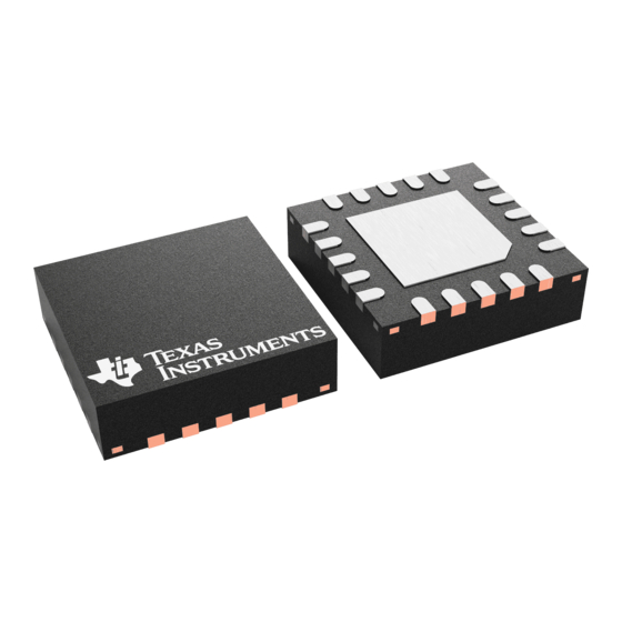
BQ77307 2-Series to 7-Series High Accuracy Battery Primary or Secondary Protector
for Li-Ion, Li-Polymer, LiFePO
1 Features
•
Primary or secondary voltage, current, and
temperature protection for 2-series to 7-series cells
with an autonomous recovery option
•
Voltage protection:
– Cell overvoltage (COV): 0 V–5.5 V in 1-mV
steps, ±4-mV accuracy
– Cell undervoltage (CUV): 0 V–5.5 V in 1-mV
steps, ±4-mV accuracy
•
Current protection:
– Short circuit in discharge (SCD): 10 mV–500
mV, varying steps
– Overcurrent in charge (OCC): 3 mV–123 mV,
2-mV steps
– Overcurrent in discharge 1 and 2 (OCD1 and
OCD2): 4 mV–200 mV, 2-mV steps
•
Temperature protection using external NTC
thermistor:
– Overtemperature in charge and discharge
(OTC and OTD)
– Undertemperature in charge and discharge
(UTC and UTD)
– Internal die overtemperature
•
Integrated low-side drivers for NFET protection
with an optional autonomous recovery
•
Low power operation:
– NORMAL mode, both FETs enabled: 8 μA
– NORMAL mode, FETs disabled: 5 μA
– SHUTDOWN Mode: < 1 μA
•
High voltage tolerance of 45 V on cell connect and
select additional pins
•
Integrated one-time-programmable (OTP) memory
for device settings, programmed by TI
•
Programmable interrupt for host processor, status
information available through I
2
•
400-kHz I
C serial communications with optional
CRC support
•
Programmable LDO for external system usage
•
20-pin QFN 3.5 mm × 3.5 mm × 0.9 mm (RGR)
package
2 Applications
•
Cordless power tools and garden tools
•
Vacuum cleaners
•
Non-military drones
•
Other industrial battery packs (2 series to 7 series)
An IMPORTANT NOTICE at the end of this data sheet addresses availability, warranty, changes, use in safety-critical applications,
intellectual property matters and other important disclaimers. PRODUCTION DATA.
(LFP), and LTO Battery Packs
4
3 Description
The Texas Instruments BQ77307 family of products
features a highly integrated, high-accuracy primary
protector for 2-series to 7-series Li-ion, Li-polymer,
LiFePO
device includes a high-accuracy voltage, current, and
temperature protection subsystem with integrated low-
side protection NFET drivers and a programmable
LDO for external system use. The BQ77307 provides
an interrupt to a host processor and integrates an
2
I
400-kHz operation with optional CRC to read status
information and program settings. The BQ77307 is
available in a 20-pin QFN package.
(1)
2
C
(LFP), and LTO battery packs. Each
4
C host communication interface, supporting up to
Device Information
PART NUMBER
PACKAGE
BQ77307
RGR (20 pins)
See the orderable addendum at the end of the data sheet.
+
+
+
VC4
+
VC3
+
VC2
+
VC1
+
VC0
TS
Simplified Schematic
BQ77307
SLUSF60 – DECEMBER 2023
PACKAGE SIZE
(1)
(NOM)
3.5 mm × 3.5 mm × 0.9
mm, 0.5-mm pitch
PACK+
External
REGOUT
Circuitry
ALERT
SDA
SCL
VSS
PACK–
Advertisement
Table of Contents

Related Manuals for Texas Instruments BQ77307


Summary of Contents for Texas Instruments BQ77307
-
Page 1: Features
BQ77307 SLUSF60 – DECEMBER 2023 BQ77307 2-Series to 7-Series High Accuracy Battery Primary or Secondary Protector for Li-Ion, Li-Polymer, LiFePO (LFP), and LTO Battery Packs 1 Features 3 Description • Primary or secondary voltage, current, and The Texas Instruments BQ77307 family of products... -
Page 2: Table Of Contents
11.5 Electrostatic Discharge Caution......7.4.4 Internal Temperature Protection......11.6 Glossary..............7.4.5 Thermistor Temperature Protections....12 Revision History............7.4.6 Protection FET Drivers........13 Mechanical, Packaging, and Orderable 7.4.7 Voltage References..........Information..............Submit Document Feedback Copyright © 2023 Texas Instruments Incorporated Product Folder Links: BQ77307... -
Page 3: Device Comparison Table
2–7 1.8 V–5.0 V PRODUCT PREVIEW 5 Pin Configuration and Functions Figure 5-1. BQ77307 Pinout Table 5-1. BQ77307 Pin Functions TYPE DESCRIPTION NAME Sense voltage input pin for the fourth cell from the bottom of the stack Sense voltage input pin for the third cell from the bottom of the stack... - Page 4 BQ77307 www.ti.com SLUSF60 – DECEMBER 2023 Table 5-1. BQ77307 Pin Functions (continued) TYPE DESCRIPTION NAME REGOUT LDO output, which can be programmed for 1.8 V, 2.5 V, 3.0 V, 3.3 V, or 5.0 V Input pin for REGOUT LDO also functions as a supply for the CHG and DSG FET REGSRC drivers.
-
Page 5: Specifications
JEDEC document JEP155 states that 500-V HBM allows safe manufacturing with a standard ESD control process. JEDEC document JEP157 states that 250-V CDM allows safe manufacturing with a standard ESD control process. Copyright © 2023 Texas Instruments Incorporated Submit Document Feedback... -
Page 6: Recommended Operating Conditions
BQ77307 THERMAL METRIC RGR (QFN) UNIT 20 PINS Junction-to-ambient thermal resistance 47.2 °C/W θJA Junction-to-case (top) thermal resistance 47.9 °C/W θJC(top) Junction-to-case (bottom) thermal resistance °C/W θJC(bottom) Submit Document Feedback Copyright © 2023 Texas Instruments Incorporated Product Folder Links: BQ77307... -
Page 7: Supply Current
BQ77307 www.ti.com SLUSF60 – DECEMBER 2023 6.4 Thermal Information BQ77307 (continued) BQ77307 THERMAL METRIC RGR (QFN) UNIT 20 PINS Junction-to-board thermal resistance 23.4 °C/W θJB Ψ Junction-to-top characterization parameter °C/W Ψ Junction-to-board characterization parameter 23.4 °C/W For more information about traditional and new thermal metrics, see the... -
Page 8: Voltage References
= -20°C to 65°C. Measured using – V ), setting = 6, positive 2516 2890 3276 µV CUR_DET_THR averaged data to remove effects of noise. threshold (charging current) Submit Document Feedback Copyright © 2023 Texas Instruments Incorporated Product Folder Links: BQ77307... - Page 9 = -20°C to 65°C. Measured using – V ), setting = 4, negative –2262 –2088 –1917 µV CUR_DET_THR averaged data to remove effects of noise. threshold (discharging current) Copyright © 2023 Texas Instruments Incorporated Submit Document Feedback Product Folder Links: BQ77307...
- Page 10 –5011 –4415 µV CUR_DET_THR averaged data to remove effects of noise. threshold (discharging current) Measurement interval 2.44 CUR_DET Specified by a combination of characterization and production test Submit Document Feedback Copyright © 2023 Texas Instruments Incorporated Product Folder Links: BQ77307...
-
Page 11: Thermistor Pullup Resistor
– 1.75 CHG FET driver rise CHG C = 20 nF, R = 100 Ω, V GATE REGSRC µs (CHG_ON) time 12 V, 0.5 V to 5 V Copyright © 2023 Texas Instruments Incorporated Submit Document Feedback Product Folder Links: BQ77307... -
Page 12: Protection Subsystem
℃ –5.8 setting, T = –20°C to 65°C Internal temperature protection (TINT_ACC) threshold accuracy Error in threshold versus nominal ℃ –7.8 setting, T = –40°C to 110°C Submit Document Feedback Copyright © 2023 Texas Instruments Incorporated Product Folder Links: BQ77307... - Page 13 Settings 21 mV to 55 mV –1.68 2.99 (OCC_ACC) threshold accuracy Overcurrent in charge (OCC) voltage Settings 57 mV to 123 mV –1.61 4.10 (OCC_ACC) threshold accuracy Copyright © 2023 Texas Instruments Incorporated Submit Document Feedback Product Folder Links: BQ77307...
-
Page 14: Timing Requirements - I
HD:STA Low period of the SCL clock µs High period of the SCL clock µs HIGH Setup repeated START µs SU:STA Data hold time (SDA input) HD:DAT Submit Document Feedback Copyright © 2023 Texas Instruments Incorporated Product Folder Links: BQ77307... -
Page 15: Timing Requirements - I
PULLUP Specified by design 6.17 Timing Diagram HD;STA SU;STA HD;STA SU;STO HIGH SU;DAT HD;DAT STOP START START REPEATED START Figure 6-1. I C Communications Interface Timing Copyright © 2023 Texas Instruments Incorporated Submit Document Feedback Product Folder Links: BQ77307... -
Page 16: Typical Characteristics
-160 -200 Temperature (°C) Temperature (°C) Figure 6-7. Overcurrent in Charge Protection Figure 6-6. Overcurrent in Discharge Protection 1 (OCC) Threshold vs. Temperature (OCD1) Threshold vs. Temperature Submit Document Feedback Copyright © 2023 Texas Instruments Incorporated Product Folder Links: BQ77307... - Page 17 BAT Current, BAT=38.5V BAT Current, BAT=6V REGSRC Current, REGSRC=25.9V BAT Current, BAT=25.9V REGSRC Current, REGSRC=30V -0.1 Temperature (°C) Figure 6-12. Supply Current in SHUTDOWN Mode vs. Temperature Copyright © 2023 Texas Instruments Incorporated Submit Document Feedback Product Folder Links: BQ77307...
-
Page 18: Detailed Description
SLUSF60 – DECEMBER 2023 7 Detailed Description 7.1 Overview The BQ77307 family is a highly integrated, accurate primary or secondary protector for 2-series to 7-series Li-ion, Li-polymer, LiFePO (LFP), and LTO battery packs. Each device includes high-accuracy voltage, current, and temperature protections, which can be triggered and recovered completely autonomously by the device or under full control of a host processor. -
Page 19: Device Security
(SCD), overcurrent in discharge 1 and 2 (OCD1, OCD2), and overcurrent in charge (OCC). 7.4.3 Unused VC Pins If the BQ77307 device is used in a system with fewer than 5 series cells, specific cells must be used for connection to real cells, as shown in Table 7-1. -
Page 20: Internal Temperature Protection
Manual. 7.4.5 Thermistor Temperature Protections The BQ77307 device supports cell temperature protections using an external thermistor on the TS pin. The device includes an internal 20-kΩ pullup resistor to bias the thermistor during evaluation. In order to provide a high precision evaluation, the device uses the same 1.8-V internal LDO voltage for the evaluation circuitry as is used for biasing the thermistor pullup resistor, thereby implementing a ratiometric operation. -
Page 21: Protection Fet Drivers
7.4.9 LDOs The BQ77307 contains an integrated 1.8-V LDO (REG18) that provides a regulated 1.8-V supply voltage for the device's internal circuitry and digital logic. The supply current for this LDO is drawn from the BAT pin. -
Page 22: Standalone Versus Host Interface
OTP settings and enable the LDO as configured, without requiring communications first. The BQ77307 is designed to operate properly with a die temperature up to 110°C, therefore the system design must avoid drawing excessive current from the REGOUT LDO if it could result in the die temperature exceeding this level. -
Page 23: I 2 C Serial Communications Interface
C serial communications interface in the BQ77307 device acts as a target device and supports rates up to 400 kHz with an optional CRC check. The BQ77307 will initially power up by default in a mode determined by the OTP settings factory programmed by TI. The host can change the CRC mode setting while in CONFIG_UPDATE mode, then the new setting will take effect upon exit of CONFIG_UPDATE mode. -
Page 24: Protection Subsystem
7.5.2 Primary Protections The BQ77307 integrates a broad suite of protections for battery management and provides the capability to enable individual protections, as well as to select which protections will result in autonomous control of the FETs. -
Page 25: Cell Open Wire Protection
The BQ77307 device supports detection of a broken connection between a cell in the pack and the cell attachment to the PCB containing the BQ77307 device. Without this check, the voltage at the cell input pin of the BQ77307 device may persist for some time on the board-level capacitor, leading to incorrect voltage readings. -
Page 26: Device Power Modes
7.6 Device Power Modes 7.6.1 Overview of Power Modes The BQ77307 device supports a normal operating mode as well as a full shutdown mode, with the device able to transition from NORMAL mode to SHUTDOWN mode autonomously, based on settings. -
Page 27: Normal Mode
SHUTDOWN, based on the configuration setting. The BQ77307 wakes from SHUTDOWN if a voltage is applied at the TS or VC0 pins above a level of approximately 1.2 V. If the shutdown sequence has been initiated, but the device detects the wakeup criteria (either the TS or VCO pin voltage detected high) is present, then the device stays in a "soft shutdown"... -
Page 28: Application And Implementation
8.1 Application Information The BQ77307 device can be used with 2-series to 7-series battery packs, supporting a top-of-stack voltage ranging from 3 V up to 38.5 V. To design and implement a comprehensive set of parameters for a specific battery pack, during development customers can use the Battery Management Studio (bqStudio), which is a graphical user-interface tool installed on a PC. - Page 29 ALERT PACK– Figure 8-1. BQ77307 7-Series Cell Typical Implementation (Simplified Schematic) A full schematic of a basic monitor circuit based on the BQ77307 for a 7-series battery pack is shown below. Section 10.2 shows the board layout for this design.
- Page 30 0.1uF 0.1uF 0.1uF MSP430F5529IPN 0.47uF 0.47uF LED3 QGND Green QGND QGND QGND 3.3V TEST Net-Tie QGND TP32 2200pF QGND Figure 8-3. BQ77307 7-Series Cell Schematic Diagram—Additional Circuitry Submit Document Feedback Copyright © 2023 Texas Instruments Incorporated Product Folder Links: BQ77307...
-
Page 31: Design Requirements
BQ77307 www.ti.com SLUSF60 – DECEMBER 2023 8.2.1 Design Requirements Table 8-1. BQ77307 Design Requirements DESIGN PARAMETER EXAMPLE VALUE Minimum system operating voltage 17.5 V Cell minimum operating voltage 2.5 V Series cell count Sense resistor 1 mΩ Thermistor in use Charge voltage 29.75 V... -
Page 32: Application Performance Plot
• Protection FET selection and configuration – The BQ77307 device is designed for use with low-side NFET protection – The configuration should be selected for series versus parallel FETs, which may lead to different FET selection for charge versus discharge direction. -
Page 33: Random Cell Connection Support
8.2.4 Random Cell Connection Support The BQ77307 device supports a random connection sequence of cells to the device during pack manufacturing. For example, cell-6 in a 7-cell stack might be first connected at the input terminals leading to pins VC6 and VC5, then cell-2 may next be connected at the input terminals leading to pins VC2 and VC1, and so on. -
Page 34: Startup Timing
CHG FET disabled, its gate voltage must drop to near this –12 V level. To support this type of case, the CHG FET driver in BQ77307 is designed to withstand voltages as low as –25 V (recommended) relative to the VSS pin voltage by including a series PFET at the pin, with its gate connected to VSS. - Page 35 Between PACK+ and PACK– A slower turn-off case is shown in Figure 8-6, using a 4.7-kΩ series gate resistor, and a 2A load between PACK+ and PACK–. Copyright © 2023 Texas Instruments Incorporated Submit Document Feedback Product Folder Links: BQ77307...
- Page 36 Figure 8-6. A Slower Turn-Off Case Using a 4.5-kΩ Series Gate Resistor A fast turn-off case is shown in Figure 8-7, in which a 100-Ω series gate resistor is used between the DSG pin and the FET gate. Submit Document Feedback Copyright © 2023 Texas Instruments Incorporated Product Folder Links: BQ77307...
-
Page 37: Usage Of Unused Pins
If not used, leave these pins floating. REGOUT REGSRC If neither the REGOUT regulator nor the CHG and DSG drivers are used, connect this pin to pin 17 (BAT). Copyright © 2023 Texas Instruments Incorporated Submit Document Feedback Product Folder Links: BQ77307... -
Page 38: Power Supply Recommendations
9 Power Supply Recommendations The BQ77307 device draws its supply current from the BAT pin, which is typically connected to the top of stack point through a series diode, to protect against any fault within the device resulting in unintended charging of the pack. -
Page 39: Layout
ESD performance. 10.2 Layout Example An example circuit layout using the BQ77307 device in a 7s-series cell design is described below. The design implements the schematic shown in the BQ77307 7-Series Cell Schematic Diagram—Monitor BQ77307 7-Series Cell Schematic Diagram—Additional Circuitry... - Page 40 BQ77307 www.ti.com SLUSF60 – DECEMBER 2023 Figure 10-2. BQ77307 Two-Layer Board Layout–Bottom Layer Submit Document Feedback Copyright © 2023 Texas Instruments Incorporated Product Folder Links: BQ77307...
-
Page 41: Device And Documentation Support
All trademarks are the property of their respective owners. 11.5 Electrostatic Discharge Caution This integrated circuit can be damaged by ESD. Texas Instruments recommends that all integrated circuits be handled with appropriate precautions. Failure to observe proper handling and installation procedures can cause damage. -
Page 42: Mechanical, Packaging, And Orderable Information
This data is subject to change without notice and revision of this document. For browser-based versions of this data sheet, refer to the left-hand navigation. Submit Document Feedback Copyright © 2023 Texas Instruments Incorporated Product Folder Links: BQ77307... - Page 43 PACKAGE OPTION ADDENDUM www.ti.com 15-Dec-2023 PACKAGING INFORMATION Orderable Device Status Package Type Package Pins Package Eco Plan Lead finish/ MSL Peak Temp Op Temp (°C) Device Marking Samples Drawing Ball material (4/5) BQ77307RGRR ACTIVE VQFN 3000 RoHS & Green NIPDAU Level-1-260C-UNLIM -40 to 110 77307...
- Page 44 PACKAGE MATERIALS INFORMATION www.ti.com 16-Dec-2023 TAPE AND REEL INFORMATION REEL DIMENSIONS TAPE DIMENSIONS B0 W Reel Diameter Cavity Dimension designed to accommodate the component width Dimension designed to accommodate the component length Dimension designed to accommodate the component thickness Overall width of the carrier tape Pitch between successive cavity centers Reel Width (W1) QUADRANT ASSIGNMENTS FOR PIN 1 ORIENTATION IN TAPE...
- Page 45 PACKAGE MATERIALS INFORMATION www.ti.com 16-Dec-2023 TAPE AND REEL BOX DIMENSIONS Width (mm) *All dimensions are nominal Device Package Type Package Drawing Pins Length (mm) Width (mm) Height (mm) BQ77307RGRR VQFN 3000 367.0 367.0 35.0 Pack Materials-Page 2...
- Page 46 GENERIC PACKAGE VIEW RGR 20 VQFN - 1 mm max height PLASTIC QUAD FLATPACK - NO LEAD 3.5 x 3.5, 0.5 mm pitch This image is a representation of the package family, actual package may vary. Refer to the product data sheet for package details. 4228482/A www.ti.com...
- Page 47 PACKAGE OUTLINE RGR0020A VQFN - 1 mm max height PLASTIC QUAD FLATPACK - NO LEAD 3.65 3.35 PIN 1 INDEX AREA 3.65 3.35 SIDE WALL METAL THICKNESS DIM A OPTION 1 OPTION 2 SEATING PLANE 0.05 0.08 C 0.00 2X 2 (DIM A) TYP SYMM EXPOSED...
- Page 48 4219031/B 04/2022 NOTES: (continued) 4. This package is designed to be soldered to a thermal pad on the board. For more information, see Texas Instruments literature number SLUA271 (www.ti.com/lit/slua271). 5. Vias are optional depending on application, refer to device data sheet. If any vias are implemented, refer to their locations shown on this view.
- Page 49 EXAMPLE STENCIL DESIGN RGR0020A VQFN - 1 mm max height PLASTIC QUAD FLATPACK - NO LEAD (0.56) TYP 20X (0.6) 20X (0.24) (0.56) TYP 16X (0.5) SYMM (3.3) 4X (0.92) (R0.05) TYP 4X (0.92) SYMM (3.3) SOLDER PASTE EXAMPLE BASED ON 0.125 MM THICK STENCIL SCALE: 20X EXPOSED PAD 21 81% PRINTED SOLDER COVERAGE BY AREA UNDER PACKAGE...
- Page 50 TI products. TI’s provision of these resources does not expand or otherwise alter TI’s applicable warranties or warranty disclaimers for TI products. TI objects to and rejects any additional or different terms you may have proposed. IMPORTANT NOTICE Mailing Address: Texas Instruments, Post Office Box 655303, Dallas, Texas 75265 Copyright © 2023, Texas Instruments Incorporated...
Need help?
Do you have a question about the BQ77307 and is the answer not in the manual?
Questions and answers