Table of Contents
Advertisement
Quick Links
www.ti.com
User's Guide
TPS54KC23EVM Step-Down Converter Evaluation Module
This user's guide contains information for the TPS54KC23EVM evaluation module and the TPS54KC23
DC/DC converter. Also included are the performance characteristics, schematic, and bill of materials for the
TPS54KC23EVM.
1
Introduction.............................................................................................................................................................................3
1.1 Background........................................................................................................................................................................
1.2 Before You Begin...............................................................................................................................................................
1.3 Performance Characteristics Summary.............................................................................................................................
Modifications.........................................................................................................................................5
2.1 Output Voltage...................................................................................................................................................................
3 Test Setup and Results..........................................................................................................................................................
3.1 Input/Output Connections..................................................................................................................................................
3.2
Efficiency............................................................................................................................................................................9
3.3 Output Voltage Regulation...............................................................................................................................................
3.4 Load Transient and Loop Response................................................................................................................................
3.5 Output Voltage Ripple......................................................................................................................................................
3.6 Start-up and Shutdown with EN.......................................................................................................................................
3.7 Thermal Performance......................................................................................................................................................
Layout.........................................................................................................................................................................14
4.1 Layout..............................................................................................................................................................................
Materials...........................................................................................................................................17
5.1 Schematic........................................................................................................................................................................
Materials.................................................................................................................................................................19
TPS54KC23EVM.......................................................................................................................................................6
Figure 3-4. U2 Efficiency - FCCM vs Skip-Mode.........................................................................................................................
Figure 3-5. U2 Efficiency - FCCM...............................................................................................................................................
Regulation.................................................................................................................................................10
Regulation..................................................................................................................................................10
Figure 3-10. U1 Transient Response.........................................................................................................................................
Figure 3-11. U2 Transient Response.........................................................................................................................................
Figure 3-12. U1 Bode Plot - 15-A Load.....................................................................................................................................
Figure 3-13. U2 Bode Plot - 15-A Load.....................................................................................................................................
Figure 3-14. U1 Output Ripple - 10-mA Load, Skip-Mode........................................................................................................
Figure 3-15. U1 Output Ripple - 30-A Load..............................................................................................................................
Figure 3-16. U2 Output Ripple - 10-mA Load, Skip-Mode........................................................................................................
Figure 3-17. U2 Output Ripple - 30-A Load..............................................................................................................................
Figure 3-18. U2 Start-up with EN - 30-A Load..........................................................................................................................
Figure 3-20. U1 Thermal Performance - 30-A Load and U2 off................................................................................................
Figure 3-21. U2 Thermal Performance - 30-A Load and U1 off................................................................................................
SLVUCU8 - JANUARY 2024
Submit Document Feedback
ABSTRACT
Table of Contents
Pin).........................................................................................................5
List of Figures
(Default)..........................................................................................................................9
(Default)..........................................................................................................................9
Load.......................................................................................................................13
Copyright © 2024 Texas Instruments Incorporated
TPS54KC23EVM Step-Down Converter Evaluation Module
Table of Contents
3
3
4
5
6
7
10
11
12
13
13
14
17
9
9
11
11
11
11
12
12
12
12
13
13
13
1
Advertisement
Table of Contents

Related Manuals for Texas Instruments TPS54KC23EVM


Summary of Contents for Texas Instruments TPS54KC23EVM
-
Page 1: Table Of Contents
User's Guide TPS54KC23EVM Step-Down Converter Evaluation Module ABSTRACT This user’s guide contains information for the TPS54KC23EVM evaluation module and the TPS54KC23 DC/DC converter. Also included are the performance characteristics, schematic, and bill of materials for the TPS54KC23EVM. Table of Contents Introduction.....................................3... - Page 2 Figure 5-2. U2 Schematic................................List of Tables Table 1-1. Input Voltage and Output Current Summary.......................3 Table 1-2. TPS54KC23EVM Small Size (U1) Performance Characteristics Summary............... Table 1-3. TPS54KC23EVM High Efficiency (U2) Performance Characteristics Summary............4 Table 2-1. MSEL Pin Selection..............................Table 3-1. Connectors and Jumpers............................7...
-
Page 3: Introduction
The following warnings and cautions are noted for the safety of anyone using or working close to the TPS54KC23EVM. Observe all safety precautions. WARNING The TPS54KC23EVM can become hot during operation due to dissipation of power in some operating conditions. Avoid contact with the board. Follow all applicable safety procedures applicable to your laboratory. -
Page 4: Performance Characteristics Summary
Introduction www.ti.com 1.3 Performance Characteristics Summary A summary of the TPS54KC23EVM performance characteristics is provided in Table 1-2 Table 1-3. The TPS54KC23EVM is designed and tested for V = 8 V to 16 V for U1 and V = 4.5 V to 16 V for U2. -
Page 5: Configurations And Modifications
11 to 12 pin shorted 64.9 Skip-mode RAMP3 13 to 14 pin shorted 75.0 Skip-mode RAMP2 15 to 16 pin shorted 86.6 Skip-mode RAMP1 Default Setting SLVUCU8 – JANUARY 2024 TPS54KC23EVM Step-Down Converter Evaluation Module Submit Document Feedback Copyright © 2024 Texas Instruments Incorporated... -
Page 6: Test Setup And Results
3 Test Setup and Results This section describes how to properly connect, set up, and use the TPS54KC23EVM evaluation module. The section also includes test results typical for the evaluation module and covers efficiency, output voltage regulation, load transients, loop response, output ripple, input ripple, start-up, and current limit modes. -
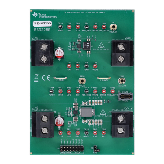
Page 7: Input/Output Connections
Test Setup and Results 3.1 Input/Output Connections The TPS54KC23EVM is provided with input connectors, output connectors, and test points as shown in Table Table 3-2. To support the minimum input voltage with the full rated load on both outputs with the default EVM, a power supply capable of supplying greater than 10 A must be connected to the VIN and PGND terminal blocks (J1 for U1, and J3 for U2) through a pair of 18-AWG wires or better. - Page 8 SMB connector to measure output voltage. When using this test point, set the TP29 VOUT_U2 scope for 1-MΩ termination. When using 50-Ω termination, a 2:1 divider is created. TPS54KC23EVM Step-Down Converter Evaluation Module SLVUCU8 – JANUARY 2024 Submit Document Feedback Copyright © 2024 Texas Instruments Incorporated...
-
Page 9: Efficiency
3.2 Efficiency Figure 3-2 through Figure 3-5 show the efficiency for both designs on the TPS54KC23EVM. The test points listed in Table 3-3 are used for the efficiency measurement. Use these test points to minimize the contribution of PCB parasitic power loss to the measured power loss. -
Page 10: Output Voltage Regulation
Iout = 30 A 0.796 0.795 Output Current (A) Input Voltage (V) Figure 3-8. U2 Load Regulation Figure 3-9. U2 Line Regulation TPS54KC23EVM Step-Down Converter Evaluation Module SLVUCU8 – JANUARY 2024 Submit Document Feedback Copyright © 2024 Texas Instruments Incorporated... -
Page 11: Load Transient And Loop Response
50000 100000200000 1000000 Frequency (Hz) Frequency (Hz) Figure 3-12. U1 Bode Plot – 15-A Load Figure 3-13. U2 Bode Plot – 15-A Load SLVUCU8 – JANUARY 2024 TPS54KC23EVM Step-Down Converter Evaluation Module Submit Document Feedback Copyright © 2024 Texas Instruments Incorporated... -
Page 12: Output Voltage Ripple
Figure 3-14 through Figure 3-17 show the TPS54KC23EVM output voltage ripple. The load currents are 10-mA and 30 A. V = 12 V. The VOUT voltage is measured using TP11 for U1 and TP29 for U2. Figure 3-14. U1 Output Ripple – 10-mA Load, Skip- Figure 3-15. -
Page 13: Start-Up And Shutdown With En
Figure 3-20. U1 Thermal Performance – 30-A Load Figure 3-21. U2 Thermal Performance – 30-A Load and U2 off and U1 off SLVUCU8 – JANUARY 2024 TPS54KC23EVM Step-Down Converter Evaluation Module Submit Document Feedback Copyright © 2024 Texas Instruments Incorporated... -
Page 14: Board Layout
Board Layout www.ti.com 4 Board Layout This section provides a description of the TPS54KC23EVM board layout and layer illustrations. 4.1 Layout The board layout for the TPS54KC23EVM is shown in Figure 4-1 through Figure 4-8. The top-side layer of the EVM is laid out in a manner typical of a user application. -
Page 15: Figure 4-3. Top Layer Layout
Figure 4-3. Top Layer Layout Figure 4-4. Mid Layer 1 Layout Figure 4-5. Mid Layer 2 Layout Figure 4-6. Mid Layer 3 Layout SLVUCU8 – JANUARY 2024 TPS54KC23EVM Step-Down Converter Evaluation Module Submit Document Feedback Copyright © 2024 Texas Instruments Incorporated... -
Page 16: Figure 4-7. Mid Layer
Board Layout www.ti.com Figure 4-7. Mid Layer 4 Layout Figure 4-8. Bottom Layer Layout TPS54KC23EVM Step-Down Converter Evaluation Module SLVUCU8 – JANUARY 2024 Submit Document Feedback Copyright © 2024 Texas Instruments Incorporated... -
Page 17: Schematic And Bill Of Materials
Schematic and Bill of Materials 5 Schematic and Bill of Materials This section presents the TPS54KC23EVM schematic and bill of materials. 5.1 Schematic Figure 5-1 is the schematic for U1. Figure 5-2 is the schematic for U2. Input: 8 V to 16 V... -
Page 18: Figure 5-2. U2 Schematic
450ohm / S MB to 50-ohm ca ble / S cope Te rm. = 50ohm 50-ohm s e rie s te rm / 50-ohm ca ble / S cope Te rm. = 1Mohm Figure 5-2. U2 Schematic TPS54KC23EVM Step-Down Converter Evaluation Module SLVUCU8 – JANUARY 2024 Submit Document Feedback... -
Page 19: Bill Of Materials
Schematic and Bill of Materials 5.2 Bill of Materials Table 5-1 details the bill of materials for the TPS54KC23EVM. Table 5-1. TPS54KC23EVM Bill of Materials DESIGNATOR VALUE DESCRIPTION PACKAGE REFERENCE PART NUMBER MANUFACTURER !PCB1 Printed Circuit Board BSR225 C1, C32 330µF... - Page 20 Schematic and Bill of Materials www.ti.com Table 5-1. TPS54KC23EVM Bill of Materials (continued) DESIGNATOR VALUE DESCRIPTION PACKAGE REFERENCE PART NUMBER MANUFACTURER 64.9k RES, 64.9 k, 1%, 0.1 W, 0603 RC0603FR-0764K9L Yageo 75.0k RES, 75.0 k, 1%, 0.1 W, 0603 RC0603FR-0775KL Yageo 86.6k...
- Page 21 STANDARD TERMS FOR EVALUATION MODULES Delivery: TI delivers TI evaluation boards, kits, or modules, including any accompanying demonstration software, components, and/or documentation which may be provided together or separately (collectively, an “EVM” or “EVMs”) to the User (“User”) in accordance with the terms set forth herein.
- Page 22 www.ti.com Regulatory Notices: 3.1 United States 3.1.1 Notice applicable to EVMs not FCC-Approved: FCC NOTICE: This kit is designed to allow product developers to evaluate electronic components, circuitry, or software associated with the kit to determine whether to incorporate such items in a finished product and software developers to write software applications for use with the end product.
- Page 23 www.ti.com Concernant les EVMs avec antennes détachables Conformément à la réglementation d'Industrie Canada, le présent émetteur radio peut fonctionner avec une antenne d'un type et d'un gain maximal (ou inférieur) approuvé pour l'émetteur par Industrie Canada. Dans le but de réduire les risques de brouillage radioélectrique à...
- Page 24 www.ti.com EVM Use Restrictions and Warnings: 4.1 EVMS ARE NOT FOR USE IN FUNCTIONAL SAFETY AND/OR SAFETY CRITICAL EVALUATIONS, INCLUDING BUT NOT LIMITED TO EVALUATIONS OF LIFE SUPPORT APPLICATIONS. 4.2 User must read and apply the user guide and other available documentation provided by TI regarding the EVM prior to handling or using the EVM, including without limitation any warning or restriction notices.
- Page 25 Notwithstanding the foregoing, any judgment may be enforced in any United States or foreign court, and TI may seek injunctive relief in any United States or foreign court. Mailing Address: Texas Instruments, Post Office Box 655303, Dallas, Texas 75265 Copyright © 2023, Texas Instruments Incorporated...
- Page 26 TI products. TI’s provision of these resources does not expand or otherwise alter TI’s applicable warranties or warranty disclaimers for TI products. TI objects to and rejects any additional or different terms you may have proposed. IMPORTANT NOTICE Mailing Address: Texas Instruments, Post Office Box 655303, Dallas, Texas 75265 Copyright © 2024, Texas Instruments Incorporated...
Need help?
Do you have a question about the TPS54KC23EVM and is the answer not in the manual?
Questions and answers