Table of Contents
Advertisement
Quick Links
Jun. 2010
Table of Contents
Distinguishing the DD-3, 3A, 3B, and 3C ......................2
Cautionary Notes ..............................................................2
Specifications .....................................................................3
Location of Controls .........................................................4
Location of Controls Parts List........................................4
Exploded View ..................................................................5
Exploded View Parts List.................................................5
Modification to the DD-3C ..............................................6
Important Notes on Assembly ........................................7
Parts List .............................................................................9
Copyright © 2010 Roland Corporation
All rights reserved. No part of this publication may be reproduced in any form without the written permission
of Roland Corporation.
Verifying the Version......................................................11
Data Backup and Restore Operations ..........................11
Performing a Factory Reset............................................11
Updating the System ......................................................11
Operation Test .................................................................11
Board)................................................................................14
Board)................................................................................16
17059557E4
SERVICE NOTES
Issued by RJA
DD-3(T)
CC-KWS
Advertisement
Table of Contents

Related Manuals for Roland DigitalDelay DD-3


Summary of Contents for Roland DigitalDelay DD-3
-
Page 1: Table Of Contents
Circuit Diagram (Main, VR, LED, Input, Output, SW Important Notes on Assembly ........7 Board)................16 Parts List ................9 Copyright © 2010 Roland Corporation All rights reserved. No part of this publication may be reproduced in any form without the written permission of Roland Corporation. 17059557E4... -
Page 2: Distinguishing The Dd-3, 3A, 3B, And 3C
• Because reissuance is restricted. • Because the part is made to order (at current market price). • Because it is carried in electronic data on the Roland web site. • Because it is a package or an accessory irrelevant to the function maintenance of the main body. -
Page 3: Specifications
Check Indicator (serves also as battery check indicator) * Printed matters will not be supplied after the end of the production. Then, download the electronic file from the Roland web site. Jacks * In the interest of product improvement, the specifications and/or appearance of this unit are subject to change without prior notice. -
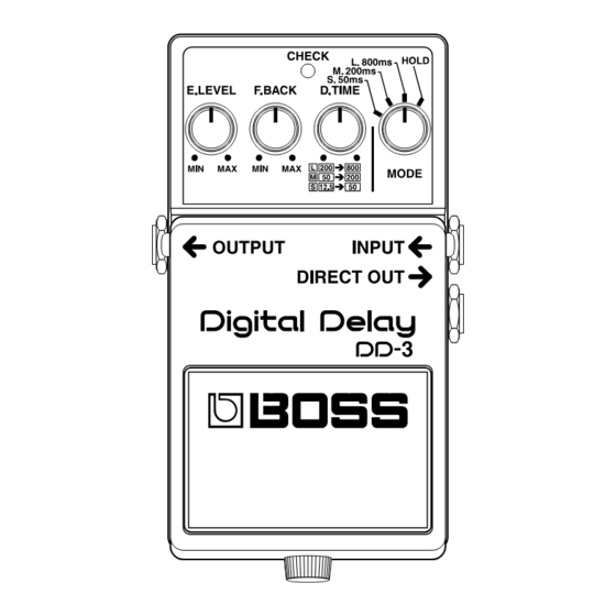
Page 4: Location Of Controls
Jun. 2010 DD-3(T) Location of Controls fig.panel.eps Location of Controls Parts List Part Code Part Name Description Q’ty 5100014487 COMPACT PSA LABEL (22537538R0) 22217404R0 PANEL 75D563C0R0 CASE (PEARL WHITE) 5100008175 R-KNOB F BLU/BLK (G2477530R0) F3279852R0 POTENTIOMETER RD901-20-15FW-B54-006 01903234 6.5MM JACK HTJ-064-13D 5100003926 PLAIN WASHER 9X13.5X0.5T... -
Page 5: Exploded View
Jun. 2010 DD-3(T) Exploded View fig.bunkaizu.eps Exploded View Parts List Part Code Part Name Description Q’ty 13129710R0 SWITCH(PUSH) JM-0404 5100007503 BATTERY CUSHION (22267333R0) 5100007872 BATTERY CONNECTOR 006P BATTERY SNAP (F3419102R0 5100006631 CAUTION SEAL PSA (FCC/EMI)(G2537516R2) 5100006633 BOTTOM FOOT (22357305R0) 5100006632 BOTTOM COVER (22027851R0) 5100007509... -
Page 6: Modification To The Dd-3C
Jun. 2010 DD-3(T) Modification to the DD-3C When modifying a DD-3, DD-3A, or DD-3B to transform it into a DD-3C, replace the respective parts shown in the table below. For the circuit boards in particular, all circuit board must be replaced at the same time. DD-3 DD-3C Part Code... -
Page 7: Important Notes On Assembly
Jun. 2010 DD-3(T) Important Notes on Assembly Installing the Output Jack Installing the Input Jack * Ensure that the wiring is not pinched. * When installing, be sure to hold down the Input Board with your hand and keep fig.assemble-1.eps the jack from tilting at an angle. - Page 8 Jun. 2010 DD-3(T) Disposition of Wiring Insert the green and orange wires behind the ribbon cable (between the Insert the Input-Board wires (brown and black) between the VR Board and the Case). potentiometer and the Input Board. fig.assemble-6.eps fig.assemble-9.eps Twist any excess length of the wires as shown in the figure. fig.assemble-10.eps Arrange the wiring as shown in the figure.
-
Page 9: Parts List
Jun. 2010 DD-3(T) Parts List fig.-part1-e.eps Due to one or more of the following reasons, Safety Precautions: parts with parts code ******** cannot be supplied as service parts. The parts marked have safety-related characteristics. Use only listed parts for replacement. •... - Page 10 Jun. 2010 DD-3(T) SCREWS 40010267 SCREW M3X10 BINDING MACHINE FE BZC 5100007965 SCREW 3X6(H5029325R0) PAN TAPPING B1 BZC 5100007512 THUMB SCREW (H5029820R0) 40128923 HEX NUT M7 5100003918 JACK NUT M9X12X2 NI RTC(H5039510R0) 5100008092 PLAIN WASHER 3X6X0.5 RESIN RTC(H5039708R0) 5100003926 PLAIN WASHER 9X13.5X0.5T NI(H5039158R0) 5100008086 INT TOOTH WASHER 9.5X12.5X0.5...
-
Page 11: Verifying The Version
Jun. 2010 DD-3(T) Verifying the Version Operation Test Turn all controls all the way counterclockwise. Items Required Hold down the pedal and insert a 1/4-inch stereo phone plug into the INPUT jack. • AC adaptor (PSA-series device) The power comes on and the CHECK LED lights up. •... - Page 12 Jun. 2010 DD-3(T) 1. Measurement of Current Consumption 3. Noise Test Make the connections as shown in the figure, then start the unit in the Make the connections as shown in the figure, then start the unit in the Test Mode. Test Mode.
- Page 13 Jun. 2010 DD-3(T) 4. MODE Test 6. BYPASS Test Make the connections as shown in the figure below, then start the unit in Make the connections as shown in the figure below, then start the unit in the normal usage state. the normal usage state.
-
Page 14: Circuit Board (Main, Vr, Led, Input, Output, Sw Board)
Jun. 2010 DD-3(T) Circuit Board (Main, VR, LED, Input, Output, SW Board) fig.b-main-1.eps... - Page 15 Jun. 2010 DD-3(T) fig.b-main-2.eps...
-
Page 16: Circuit Diagram (Main, Vr, Led, Input, Output, Sw Board)
Jun. 2010 DD-3(T) Circuit Diagram (Main, VR, LED, Input, Output, SW Board) fig.d-main.eps@L DD-3C Circuit Diagram MAIN BOARD F2917014R0 1/6 ASSY 75D573P0R0 AVCC AVCC UnPop AVREF AGND NJM4558M(TE3) BROWN TP500 TP65 TP501 R200 TP502 D ( 0.5% ) 0.1uF BLACK HTJ-064-13D TP31 TP503... - Page 17 Jun. 2010 DD-3(T) fig.d-main.eps@R * The symbols appearing at the TP locations are silkscreened on the circuit board. Identical symbols are mutually connected by wiring. TP200 TP53 C127 68pF 2200pF D ( 0.5% ) OUTPUT BOARD F2917014R0 5/6 D ( 0.5% ) 2SK879-Y(TE85R.F) ASSY 75D573P0R0 TP211...
Need help?
Do you have a question about the DigitalDelay DD-3 and is the answer not in the manual?
Questions and answers