Advertisement
Quick Links
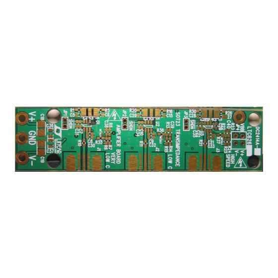
Description
Demonstration Circuit 2414A has layouts for three chan-
nels of SOT-23 transimpedance amplifiers. Each of the
three layouts applies different techniques achieving
various parasitic feedback capacitances (C
channel, U3, assumes a low Transimpedance gain, has
a parasitic C
of 0.1pF, and provides a footprint for an
F
additional component C
lower channel, U1, assumes high transimpedance gain and
was laid out to minimize C
although the real situation is more complex. The middle
channel, U2, assumes a middle case. The outputs of the
circuit are laid out for SMA edge connectors. The inputs
consist of six pads per channel along the edge where a
through-hole photodiode can be mounted, with provision
BoarD photo
Arrow.com.
Downloaded from
). The upper
F
in an 0402 footprint (C29). The
F
, achieving approximately 7fF ,
F
Figure 1. Topside Bare PCB DC2414A, for SOT-23 LTC
DEMO MANUAL DC2414A
LTC6268 and LTC6268-10
3-Channel SOT-23
Transimpedance Amplifier
for any photodiode pinout. The reverse bias voltage for
the photodiode can be applied at a V
+
–
taken from V
or V
through jumper JP4. The V
were spaced according to IPC2221 for 150V working volt-
age, so high voltage APDs can be applied. Take caution
when working with high voltages to avoid contact with
any part of the VBB trace. Because of the many possible
varieties of population, the board is stocked as a bare
unpopulated board.
Design files for this circuit board are available at
http://www.linear.com/demo/DC2414A
L, LT, LTC, LTM, Linear Technology and the Linear logo are registered trademarks of Linear
Technology Corporation. All other trademarks are the property of their respective owners.
6268 and LTC6268-10 Op Amps
®
turret, or can be
BB
traces
BB
dc2414af
1
Advertisement

Subscribe to Our Youtube Channel
Related Manuals for Linear Technology DC2414A


Summary of Contents for Linear Technology DC2414A
- Page 1 SMA edge connectors. The inputs consist of six pads per channel along the edge where a L, LT, LTC, LTM, Linear Technology and the Linear logo are registered trademarks of Linear Technology Corporation. All other trademarks are the property of their respective owners.
-
Page 2: Operating Principles
DEMO MANUAL DC2414A operating principles LTC6268 LTC6268-10 have gain bandwidth prod- But the resistor and its pads also have parasitic capaci- ucts of 500MHz and 4GHz respectively. At low transimped- tance. For example, a typical 0805 resistor has about 70fF... - Page 3 3GHz of bandwidth. The photodiode reverse bias can be applied at the V The DC2414A high speed channel was designed with turret. (Note that all “turrets” are close to the edges of the little ground copper in the photodiode region, to support board, so clips can be applied directly to the plated holes, the lowest input capacitance possible.
- Page 4 DEMO MANUAL DC2414A sample population Figure 3. An Example of a Population of the Very Low Capacitance Channel Around U1. Photodiode is OSI FCI-125G-006HRL, Anode Connected to the TIA Input, so Cathode is Held High to V Shorted to V is 9.76M on the Bottom Side (Left)
-
Page 5: Schematic Diagram
Information furnished by Linear Technology Corporation is believed to be accurate and reliable. However, no responsibility is assumed for its use. Linear Technology Corporation makes no representa- tion that the interconnection of its circuits as described herein will not infringe on existing patent rights. - Page 6 Linear Technology Corporation (LTC) provides the enclosed product(s) under the following AS IS conditions: This demonstration board (DEMO BOARD) kit being sold or provided by Linear Technology is intended for use for ENGINEERING DEVELOPMENT OR EVALUATION PURPOSES ONLY and is not provided by LTC for commercial use. As such, the DEMO BOARD herein may not be complete in terms of required design-, marketing-, and/or manufacturing-related protective considerations, including but not limited to product safety measures typically found in finished commercial goods.
Need help?
Do you have a question about the DC2414A and is the answer not in the manual?
Questions and answers