Table of Contents
Advertisement
Quick Links
MT9P111PACSTCH-GEVB
MT9P111 Evaluation Board
User's Manual
Evaluation Board Overview
The evaluation boards are designed to demonstrate the features of
ON Semiconductor's image sensors products. This headboard is
intended to plug directly into the Demo 3 system. Test points and
jumpers on the board provide access to the clock, I/Os, and other
miscellaneous signals.
Features
•
Clock Input
Default – 27 MHz Crystal Oscillator
♦
Optional Demo 3 Controlled MClk
♦
•
Two Wire Serial Interface
Selectable Base Address
♦
•
Parallel Interface
•
MIPI Interface
•
ROHS Compliant
Block Diagram
Programming
Voltage
Vpp
Connector
XMCLK,
nReset,
Clock and
STDBY,
Control Signals
Shutdown
Supplied from
Dome 2
SCL
SDA
2-Wire from
Demo 2
+5 V from
Demo 2
Figure 2. Block Diagram of MT9P111PACSTCH−GEVB
© Semiconductor Components Industries, LLC, 2015
September, 2015 − Rev. 0
8/10 Bit
Parallel Data
Pixel Clock
Connector
LV, FV
HS Serial
CLK/Data
MT9P111
Connector
VGPIO (0−7)
Connector
S_SCL
Multi-Master
S_SDA
Connector
+1.8 V, +2.8 Vana,
+2.8 Vdig
Voltage
Regulators
EVAL BOARD USER'S MANUAL
26-Pin
Demo 2
MIPI
Adapter
Board
VGPIO
User
2-Wire
Figure 1. MT9P111 Evaluation Board
1
www.onsemi.com
Publication Order Number:
EVBUM2312/D
Advertisement
Table of Contents

Related Manuals for ON Semiconductor MT9P111


Summary of Contents for ON Semiconductor MT9P111
- Page 1 User's Manual Evaluation Board Overview The evaluation boards are designed to demonstrate the features of ON Semiconductor’s image sensors products. This headboard is www.onsemi.com intended to plug directly into the Demo 3 system. Test points and jumpers on the board provide access to the clock, I/Os, and other EVAL BOARD USER’S MANUAL...
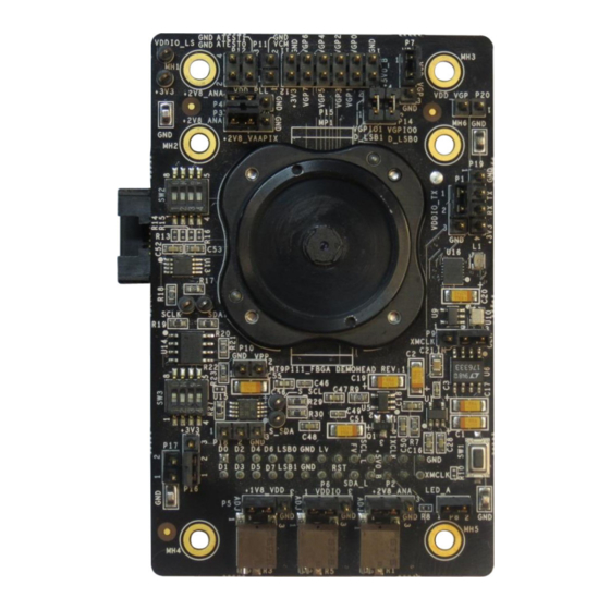
- Page 2 MT9P111PACSTCH−GEVB Top View VCM P11 +VDD_VGPIO P7 ATEST P12 +VDD_PLL P4 UART Control P20 +2V8_VAAPIX P3 DOUTLSB P14 Configuration Switch SW2 UART Connector P19 +VDDIO_TX P1 CLK_SELECT P9 +VPP P10 EEPROM ADDR SW3 C Debug P18 RESET Switch SW1 +3V3 P16 ON_LED P8 +1V8_VDD P5 +2V8_ANA P2...
- Page 3 MT9P111PACSTCH−GEVB Jumper Pin Location The jumpers on headboards start with Pin 1 on the leftmost side of the pin. Grouped jumpers increase in pin size with each jumper added. Pin 1 Pins 1−4 Figure 5. Pin Locations for a Single Jumper. Pin 1 is Located at the Leftmost Side and Increases as it Moves to the Right Pin 1 Pins 1 and 2...
- Page 4 MT9P111PACSTCH−GEVB Jumper/Header Functions & Default Positions Table 1. JUMPERS AND HEADERS Jumper/Header No. Jumper/Header Name Pins Description +VDDIO_TX 1−2 (Default) Connects to On-Board +VDDIO_TX Power Supply 2−3 External Power Supply Connection +VAA 1−2 (Default) Connects to On-Board +2V8_ANA Power Supply 2−3 External Power Supply Connection +VAAPIX...
- Page 5 MT9P111PACSTCH−GEVB Interfacing to ON Semiconductor Demo 2y Baseboard The ON Semiconductor Demo 2× baseboard has a similar The four mounting holes secure the baseboard and the 26-pin connector which mates with P13 of the headboard. headboard with spacers and screws.
- Page 6 onsemi, , and other names, marks, and brands are registered and/or common law trademarks of Semiconductor Components Industries, LLC dba “onsemi” or its affiliates and/or subsidiaries in the United States and/or other countries. onsemi owns the rights to a number of patents, trademarks, copyrights, trade secrets, and other intellectual property. A listing of onsemi’s product/patent coverage may be accessed at www.onsemi.com/site/pdf/Patent−Marking.pdf.
Need help?
Do you have a question about the MT9P111 and is the answer not in the manual?
Questions and answers