Table of Contents
Advertisement
Quick Links
MT9P017LACSTCH-GEVB
MT9P017 Evaluation Board
User's Manual
Evaluation Board Overview
The evaluation boards are designed to demonstrate the features of
ON Semiconductor's image sensors products. This headboard is
intended to plug directly into the Demo 2X system. Test points and
jumpers on the board provide access to clock, I/Os and other
miscellaneous signals.
Features
•
Clock Input
Default − 24 MHz crystal oscillator
♦
Optional Demo 2X controlled MClk
♦
•
Two Wire Serial Interface
Selectable base address
♦
•
Parallel Interface
•
MIPI Interface
•
ROHS Compliant
Block Diagram
I2C BUS
REPEATER
© Semiconductor Components Industries, LLC, 2016
July, 2016 − Rev. 0
SENSOR
SENSOR I2C BUS
MIPI CLOCK
MIPI DATA
JUMPER SELECT
VDD, VDDPLL +om
VDD 1V2, VREGO VT
2 X RJ45
VOLTAGE
REGULATORS
Figure 2. Block Diagram of MT9P017LACSTCH−GEVB
EVAL BOARD USER'S MANUAL
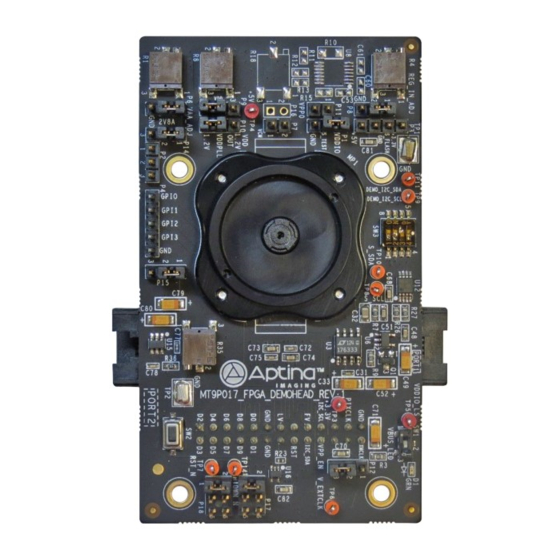
Figure 1. MT9P017 Evaluation Board
VOLTAGE LEVEL
SHIFTER
D[11:0] PIXCLK
LV
FV
VOLTAGE
FOLLOWER
5V
I2C BUS
1
www.onsemi.com
DEMO 2
CONNECTOR
Publication Order Number:
EVBUM2447/D
Advertisement
Table of Contents

Related Manuals for ON Semiconductor MT9P017LACSTCH-GEVB


Summary of Contents for ON Semiconductor MT9P017LACSTCH-GEVB
- Page 1 Evaluation Board Overview The evaluation boards are designed to demonstrate the features of www.onsemi.com ON Semiconductor’s image sensors products. This headboard is intended to plug directly into the Demo 2X system. Test points and EVAL BOARD USER’S MANUAL jumpers on the board provide access to clock, I/Os and other miscellaneous signals.
- Page 2 MT9P017LACSTCH−GEVB Top View +1V2_VDDPLL P10 +1V2_VDD P9 +VPP P11 +2V8_VAA P6 +1V8_REG_IN P8 +2V8_VAAPIX P14 FLASH P3 ATEST P2 SAADR P1 +VCM P7 GPIO P4 EEPROM SW3 +VDDIO P15 RESET Switch SW2 S_XSHTDN P17 MCLK_IN P12 S_RST_N P18 Figure 3. Top View of Evaluation Board − Default Jumpers Bottom View MIPI Connector J1 MIPI Connector J2...
- Page 3 MT9P017LACSTCH−GEVB Jumper Pin Locations The jumpers on headboards start with Pin 1 on the leftmost side of the pin. Grouped jumpers increase in pin size with each jumper added. Pin 1 Pins 1−4 Figure 5. Pin Locations for a Single Jumper. Pin 1 is Located at the Leftmost Side and Increases as it Moves to the Right Pin 1 Pins 1 and 2...
- Page 4 A0 on, A1 on, EEPROM Address set to 0xA0 A2 on, WP on Interfacing to ON Semiconductor Demo 2X Baseboard on a given power rail, cut the trace between the two pins of The ON Semiconductor Demo 2X baseboard has their respective JP, and insert an ammeter prior to powering a similar 26-pin which mates with P13 of the headboard.
- Page 5 LIMITATIONS OF LIABILITY: ON Semiconductor shall not be liable for any special, consequential, incidental, indirect or punitive damages, including, but not limited to the costs of requalification, delay, loss of profits or goodwill, arising out of or in connection with the board, even if ON Semiconductor is advised of the possibility of such damages. In no event shall ON Semiconductor’s aggregate liability from any obligation arising out of or in connection with the board, under any theory of liability, exceed the purchase price paid for the board, if any.
Need help?
Do you have a question about the MT9P017LACSTCH-GEVB and is the answer not in the manual?
Questions and answers