Table of Contents
Advertisement
Quick Links
MT9P011I12STCH-GEVB
MT9P011 Evaluation Board
User's Manual
Evaluation Board Overview
The evaluation boards are designed to demonstrate the features of
ON Semiconductor's image sensors products. This headboard is
intended to plug directly into the Demo 2X system. Test points and
jumpers on the board provide access to clock, I/Os and other
miscellaneous signals.
Features
•
Clock Input
Default − 24 MHz crystal oscillator
♦
Optional Demo 2X controlled MClk
♦
•
Two Wire Serial Interface
Selectable base address
♦
•
Parallel Interface
•
Serial LVDS Interface
•
ROHS Compliant
Block Diagram
© Semiconductor Components Industries, LLC, 2016
July, 2016 − Rev. 0
Figure 2. Block Diagram of MT9P011I12STCH−GEVB
EVAL BOARD USER'S MANUAL
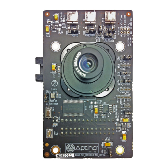
Figure 1. MT9P011 Evaluation Board
1
www.onsemi.com
Publication Order Number:
EVBUM2446/D
Advertisement
Table of Contents

Related Manuals for ON Semiconductor MT9P011


Summary of Contents for ON Semiconductor MT9P011
- Page 1 Evaluation Board Overview The evaluation boards are designed to demonstrate the features of www.onsemi.com ON Semiconductor’s image sensors products. This headboard is intended to plug directly into the Demo 2X system. Test points and EVAL BOARD USER’S MANUAL jumpers on the board provide access to clock, I/Os and other miscellaneous signals.
- Page 2 MT9P011I12STCH−GEVB Top View VDDPLL P3 VAA P1 VDD P5 VDDIO P4 VAAPIX P2 OE_N P33 TRIGGER P34 STANDBY P35 SEN_SADDR P25 SCAN_EN P39 CLKGEN P20 FLASH P37 EEPROM P14, P15 RESET Switch SW3 ON_LED P11 Figure 3. Top View of Evaluation Board − Default Jumpers Bottom View Serial LVDS Connector J3 Baseboard Connector P36...
- Page 3 MT9P011I12STCH−GEVB Jumper Pin Locations The jumpers on headboards start with Pin 1 on the leftmost side of the pin. Grouped jumpers increase in pin size with each jumper added. Pin 1 Pins 1−4 Figure 5. Pin Locations for a Single Jumper. Pin 1 is Located at the Leftmost Side and Increases as it Moves to the Right Pin 1 Pins 1 and 2...
- Page 4 RESET When pushed, 240 ms reset signal will be sent to MT9P011 Interfacing to ON Semiconductor Demo 2X Baseboard up the system. The figure below shows where the trace to cut The ON Semiconductor Demo 2X baseboard has is located.
- Page 5 onsemi, , and other names, marks, and brands are registered and/or common law trademarks of Semiconductor Components Industries, LLC dba “onsemi” or its affiliates and/or subsidiaries in the United States and/or other countries. onsemi owns the rights to a number of patents, trademarks, copyrights, trade secrets, and other intellectual property. A listing of onsemi’s product/patent coverage may be accessed at www.onsemi.com/site/pdf/Patent−Marking.pdf.
Need help?
Do you have a question about the MT9P011 and is the answer not in the manual?
Questions and answers