
Subscribe to Our Youtube Channel
Related Manuals for Protech Systems SP-6265 M1


Summary of Contents for Protech Systems SP-6265 M1
- Page 1 USER MANUAL SP-6265 15” Fanless Panel PC Powered by Intel Core ® i7/i5/i3 / Pentium / Celeron ® ® CPU Processor SP-6265 M1...
- Page 2 SP-6265 15” High Performance Panel PC COPYRIGHT NOTICE & TRADEMARK All trademarks and registered trademarks mentioned herein are the property of their respective owners. This manual is copyrighted in Feb. 2018. You may not reproduce or transmit in any form or by any means, electronic, or mechanical, including photocopying and recording.
- Page 3 FCC NOTICE This equipment has been tested and found to comply with the limits for a Class A digital device, pursuant to part 15 of the FCC Rules. These limits are designed to provide reasonable protection against harmful interference when the equipment is operated in a commercial environment.
-
Page 4: Table Of Contents
Contents Revision History .................... vi Introduction ..................1-1 About This Manual ..............1-2 Getting Started ..................2-1 Package List ................2-2 System Overview ............... 2-3 System Specifications ..............2-6 Safety Precautions ..............2-8 System Configuration ................. 3-1 External I/O Ports Diagram ............3-2 SP-6265 Bottom I/O Ports Diagram ........... - Page 5 3.7.5 Digital Input/Output Connector (For SP-6265Rx-x1x) (optional) 3-18 3.7.6 Digital Input/Output Connector (For SP-6265Rx-x0x) (optional) 3-19 3.7.7 DVI-I Port ................3-20 3.7.8 HD Audio Connector ............3-21 3.7.10 Mini PCI Express Slots ............. 3-22 3.7.11 Serial ATA (SATA) 3.0 Connectors ........3-24 3.7.12 SATA Power Connectors ...........
- Page 6 3.7.33 Clear CMOS Data Selection ..........3-41 TOUCH CONTROL BOARD SR-6145 CONNECTOR QUICK REFERENCE TABLE ............... 3-42 TOUCH CONTROL BOARD SR-6145 COMPONENT LOCATIONS ................3-42 3.9.1 Touch Control Board SR-6145 Top View ......3-42 3.10 SETTING TOUCH CONTROL BOARD SR-6145 CONNECTORS AND JUMPERS ...............
- Page 7 Installing Graphics Driver Utility ..........4-10 Installing LAN Driver Utility ............4-11 Installing Sound Driver Utility ........... 4-12 4.10 Installing Touch Driver Utility ............ 4-12 4.11 Microsoft Hotfix kb3211320 and kb3213986 Driver installation ...................... 4-13 BIOS SETUP ..................5-1 Introduction.................
- Page 8 Boot ..................5-40 5.7.1 Boot – Network Device BBS Priorities ......5-42 5.7.2 Boot – Hard Drive BBS Priorities ........5-43 5.7.3 Boot – CSM Configuration ..........5-44 Save & Exit ................5-46 Appendix A System Diagrams ............ A-1 SP-6265 Equipped Module PC Exploded Diagram ........A-2 SP-6265 LCD Display Exploded Diagram ..........A-3 SP-6265 Module PC Exploded Diagram ..........A-5 SP-6265 1st Memory Slot &...
-
Page 9: Revision History
Revision History The revision history of SP-6265 User Manual is described below: Version No. Revision History Page No. Date Initial Release 2018/01/22... -
Page 10: Introduction
Introduction This chapter provides the introduction for the SP-6265 system as well as the framework of the user manual. The following topic is included: • About This Manual Page: 1-1 SP-6265 SERIES USER MANUAL... -
Page 11: About This Manual
Chapter 1 Introduction 1.1 About This Manual Thank you for purchasing our SP-6265 system. The SP-6265 is an updated system designed to be comparable with the highest performance of IBM AT personal computers. The SP-6265 provides faster processing speed, greater expandability and can handle more tasks than before. -
Page 12: Getting Started
Getting Started This chapter provides the information for the SP-6265 system. It describes how to set up the system quickly and outlines the system specifications. The following topics are included: • Package List • System Overview • System Specification • Safety Precautions Experienced users can go to Chapter 3 System Configuration on page 3-1 for a quick start. -
Page 13: Package List
Chapter 2 Getting Started 2.1 Package List If you discover any of the items listed below are damaged or lost, please contact your local distributor immediately. Item Q’ty SP-6265 Manual / Driver DVD Quick Guide Page: 2-2 SP-6265 SERIES USER MANUAL... -
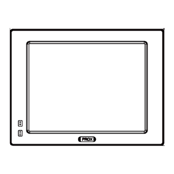
Page 14: System Overview
Chapter 2 Getting Started 2.2 System Overview Unit: mm SP-6265 Front View Rear View Top View SP-6265 SERIES USER MANUAL Page: 2-3... - Page 15 Chapter 2 Getting Started Side View Page: 2-4 SP-6265 SERIES USER MANUAL...
- Page 16 Chapter 2 Getting Started Bottom View Quarter View Page: 2-5 SP-6265 SERIES USER MANUAL...
-
Page 17: System Specifications
Chapter 2 Getting Started 2.3 System Specifications System Intel Core i7-6700TE, Quad Core, 2.4GHz, 8M cache Intel Core i5-6500TE, Quad Core, 2.3GHz, 6M cache Intel Core CPU Support i3-6100TE, Quad Core, 2.7GHz, 4M cache ® Intel Pentium G4400TE,Dual Core, 2.4GHz, 3M cache ®... - Page 18 Chapter 2 Getting Started ® LAN 1: Intel PHY I219 LM (10/100/1000 Mbps) ® LAN 2: Intel LAN I210 AT (10/100/1000 Mbps) 8 in / 8 out, DSUB-25 type or 16-pin terminal block Digital I/O Port (optional) ...
-
Page 19: Safety Precautions
Chapter 2 Getting Started 2.4 Safety Precautions Before operating this system, read the following information carefully to protect your systems from damages, and extend the life cycle of the system. Check the Line Voltage • The operating voltage for the power supply should be within the range of 100V to 240V AC;... -
Page 20: System Configuration
System Configuration This chapter contains helpful information about the jumper & connector settings, and component locations for the main board. The following topics are included: • SP-6265 Bottom I/O Ports Diagrams • Connector & Jumper Quick Reference Table • System Main Board Component Locations •... -
Page 21: External I/O Ports Diagram
Chapter 3 System Configuration 3.1 External I/O Ports Diagram 3.2 SP-6265 Bottom I/O Ports Diagram For SP-6265Rx-x0x Remote DC IN DVI-I COM3 COM1 USB 3.0 MIC-in Switch Line-out Power COM4 COM2 Button Line-in POE ON For SP-6265Rx-x1x Remote USB 3.0 DVI-I COM3 COM1... -
Page 22: Jumper & Connector Quick Reference Table
Chapter 3 System Configuration 3.3 Jumper & Connector Quick Reference Table CONNECTOR Description NAME Clear CMOS Data Selection CMOS1 LVDS Panel Selection JP1, JP2 LVDS Power Selection BIOS Recovery Mode Selection Flash Descriptor Override Selection CFast Voltage Control Selection COM1 Pin9 RI/5V/12V Selection JP12 COM2 Pin18 RI/5V/12V Selection JP15... - Page 23 Chapter 3 System Configuration CONNECTOR Description NAME Panel Power LED Connector PWRLED1 Panel HDD LED Connector HDDLED1 Low Pin Count (LPC) Connector JLPC1 CFast Card Slot CFAST1 DDR4 SO-DIMM memory socket SO-DIMM1 Mainboard Rear Side Connector SIM Card Slot SIM1 DDR4 SO-DIMM memory socket SO-DIMM2 Page: 3-4...
-
Page 24: Component Locations Of System Main Board
Chapter 3 System Configuration 3.4 Component Locations Of System Main Board 3.4.1 Top View and Jumper Settings of SB-8400 CFast Voltage Control Selection 3.3V (default) 20 19 RST_SW1 Hardware Power Failure Selection SATA_PWR1 SATA_PWR2 PWR_BTN1 JLPC1 PWR_BTN2 SATA1 SATA2 M_PCIE2 CFAST1 HDDLED1 PCI_E1... - Page 25 Chapter 3 System Configuration WARNING: Always disconnect the power cord when you are working with connectors and jumpers on the main board. Make sure both the system and peripheral devices are turned OFF as sudden surge of power could damage sensitive components.
-
Page 26: Bottom View Of Sb-8400
Chapter 3 System Configuration 3.4.2 Bottom View of SB-8400 Figure 3-2 Main Board Component Location (Rear View) Page: 3-7 SP-6265 SERIES USER MANUAL... -
Page 27: How To Set Jumpers
Chapter 3 System Configuration 3.5 How To Set Jumpers You can configure your board by setting the jumpers. A jumper consists of two or three metal pins with a plastic base mounted on the card. By using a small plastic "cap", also known as the jumper cap (with a metal contact inside), you are able to connect the pins. - Page 28 Chapter 3 System Configuration Jumper diagrams Jumper settings Page: 3-9 SP-6265 SERIES USER MANUAL...
-
Page 29: Function Buttons And I/O Ports
Chapter 3 System Configuration 3.6 Function Buttons and I/O Ports 3.6.1 Power Button Press the Power button located on the left side of Bottom I/O panel. ACTION ASSIGNMENT Press Release PWRBTN Power Button 3.6.2 DC IN Port (For SP-6265Rx-x0x) Port Name: DC IN Description: DC Power-In Port ASSIGNMENT ASSIGNMENT... -
Page 30: Dc In 3 Pins Terminal Block (For Sp-6265Rx-X1X)
Chapter 3 System Configuration DC IN 3 Pins Terminal Block (For SP-6265Rx-x1x) 3.6.3 Port Name: DC IN Description: DC IN 3 pins terminal block ASSIGNMENT VCC: 9 ~ 36 VDC DC IN Note: The 3-pin DC IN terminal block is not supported in SP-6265Rx-x0x. Page: 3-11 SP-6265 SERIES USER MANUAL... -
Page 31: Setting Connectors And Jumpers
Chapter 3 System Configuration 3.7 Setting Connectors and Jumpers 3.7.1 COM Port COM1(RS232/RS422/RS485) Connector Pin Assignment: ASSIGNMENT RS232 RS422 RS485 (Default Setting) DCD# RS-485- COM1 RS-485+ DTR# DSR# RTS# CTS# COM2(RS232/RS422/RS485) Connector Pin Assignment: ASSIGNMENT RS232 RS422 RS485 (Default Setting) DCD# RS-485- COM2... - Page 32 Chapter 3 System Configuration COM3(RS232) Connector Pin Assignment: ASSIGNMENT ASSIGNMENT DCD# DSR# RTS# COM3 CTS# DTR# COM4(RS232) Connector Pin Assignment: ASSIGNMENT ASSIGNMENT DCD# DSR# RTS# CTS# COM4 DTR# Page: 3-13 SP-6265 SERIES USER MANUAL...
-
Page 33: Com1 Pin9 And Com2 Pin18 Definition Selection Guide3-14
Chapter 3 System Configuration 3.7.2 COM1 Pin9 and COM2 PIN18 Definition Selection Guide Jumper Location: JP12, JP15 Description: COM1 pin9 (JP12) and COM2 pin18 (JP15) RI/5V/12V Selection SELECTION JUMPER SETTING JUMPER ILLUSTRATION (Default Setting) JP12 JP15 +12V JP12 JP15 JP15 JP12 Page: 3-14 SP-6265 SERIES USER MANUAL... -
Page 34: Lan1, Lan2 Ports
Chapter 3 System Configuration 3.7.3 LAN1, LAN2 Ports Port Name: LAN1, LAN2 Description: LAN1, LAN2 Port, LAN RJ-45 Port (Bottom I/O) • ® LAN1: Intel PHY I219 LM (10/100/1000Mbps) • ® LAN2: Intel LAN I210 AT (10/100/1000Mbps) ASSIGNMENT MDI_1D0+ MDI_1D0- MDI_1D1+ MDI_1D1- MDI_1D2+... - Page 35 Chapter 3 System Configuration LAN1 / LAN2 Status There are LAN LED indicators on the bottom side of the system. By observing their status, you can know the status of the Ethernet connection. LAN LED Indicator Left Side LED Green Color On 10/100Mbps LAN Speed Indicator Yellow Color On Giga LAN Speed Indicator...
-
Page 36: X 1 Usb 3.0 Connectors
Chapter 3 System Configuration 3.7.4 4 x 1 USB 3.0 Connectors Port Name: USB1 Description: USB 3.0 Ports x 4 USB 3.0 signals: ASSIGNMENT ASSIGNMENT USB3_TX1+ USB_D1- USB3_TX1- USB_D1+ USB3_RX1+ USB3_RX1- VCC5 USB3_TX2+ USB_D2- USB3_TX2- USB_D2+ USB3_RX2+ USB3_RX2- USB3_TX3+ USB_D3- USB3_TX3- USB_D3+ USB1... - Page 37 Chapter 3 System Configuration 3.7.5 Digital Input/Output Connector (For SP-6265Rx-x1x) (optional) Connector Location: DIO1 Description: M/B DIO Port Connector 16 pins ASSIGNMENT ASSIGNMENT DIN1 DOUT1 DIO1 DIN2 DOUT2 DIN3 DOUT3 DIN4 DOUT4 DIN5 DOUT5 DIN6 DOUT6 DIN7 DOUT7 DIN8 DOUT8 System Digital I/O Port DSUB-25 pins (bottom I/O) ASSIGNMENT ASSIGNMENT...
-
Page 38: Digital Input/Output Connector (For Sp-6265Rx-X0X) (Optional)
Chapter 3 System Configuration 3.7.6 Digital Input/Output Connector (For SP-6265Rx-x0x) (optional) Connector Location: DIO1 Description: M/B DIO Port Connector 16 pins ASSIGNMENT ASSIGNMENT DIN1 DOUT1 DIO1 DIN2 DOUT2 DIN3 DOUT3 DIN4 DOUT4 DIN5 DOUT5 DIN6 DOUT6 DIN7 DOUT7 DIN8 DOUT8 System 16 pins terminal block DIO Port ASSIGNMENT DIN1... -
Page 39: Dvi-I Port
Chapter 3 System Configuration 3.7.7 DVI-I Port Connector Location: DVI1 Description: DVI (Digital Visual Interface) Integrated Connector DVI1 ASSIGNMENT ASSIGNMENT TMDS_D2- TMDS_D2+ TMDS_HPD TMDS_D0- TMDS_CLK TMDS_D0+ TMDS_DATA VSYNC TMDS_D1- TMDS_D1+ TMDS_D3+ TMDS_D3- GREEN BLUE HSYNC Page: 3-20 SP-6265 SERIES USER MANUAL... -
Page 40: Hd Audio Connector
Chapter 3 System Configuration 3.7.8 HD Audio Connector Connector Location: AUDIO1 Description: HD Audio Connector for Line_in/Line_out/Mic_in. ASSIGNMENT MIC_IN_L MIC_IN_R LINE_OUT_L LINE_OUT_R LINE_IN_L LINE_IN_R AUDIO1 Page: 3-21 SP-6265 SERIES USER MANUAL... -
Page 41: Mini Pci Express Slots
Chapter 3 System Configuration 3.7.10 Mini PCI Express Slots Connector Location: M_PCIE1 and M_PCIE2 Description: Mini-PCI Express Slots Full-Sized Mini-PCI Express Slot 1 (M_PCIE1) signals: ASSIGNMENT ASSIGNMENT WAKE# +3.3V_SB +1.5V CLKREQ# SIM_PWR M_PCIE1/ SIM_DAT M_PCIE2 REFCLK+ SIM_CLK REFCLK- SIM_RST SIM_VPP SIM_SW1 SIM_SW2 PERST#... - Page 42 Chapter 3 System Configuration Half-Sized Mini-PCI Express Slot 2 (M_PCIE2) signals: ASSIGNMENT ASSIGNMENT WAKE# +3.3V_SB +1.5V CLKREQ# REFCLK+ REFCLK- PERST# PE_RX8- +3.3V_SB PE_RX8+ +1.5V SMB_CLK PE_TX8- SMB_DATA PE_TX8+ USB_D10- USB_D10+ +3.3V_SB +3.3V_SB +1.5V +3.3V_SB Mini PCI Express is the successor of the Mini PCI card and provides an increased data throughput.
-
Page 43: Serial Ata (Sata) 3.0 Connectors
Chapter 3 System Configuration 3.7.11 Serial ATA (SATA) 3.0 Connectors Connector Location: SATA1 and SATA2 Description: Serial ATA 3.0 Connectors Serial ATA 3.0 Connector 1 (SATA1) signals: ASSIGNMENT SATA_TX+ SATA_TX- SATA_RX- SATA_RX+ SATA1/ SATA2 Serial ATA 3.0 Connector 2 (SATA2) signals: ASSIGNMENT SATA_TX1+ SATA_TX1-... -
Page 44: Sata Power Connectors
Chapter 3 System Configuration 3.7.12 SATA Power Connectors Connector Location: SATA_PWR1 and SATA_PWR2 Description: Serial ATA Power Connectors Serial ATA Power Connector 1 (SATA_PWR1) signals: ASSIGNMENT Serial ATA Power Connector 2 (SATA_PWR2) signals: ASSIGNMENT SATA_PWR1/ SATA_PWR2 Page: 3-25 SP-6265 SERIES USER MANUAL... -
Page 45: Power Input Connector
Chapter 3 System Configuration 3.7.13 Power Input Connector Connector Location: PWR_IN1 Description: Power Input Connector ASSIGNMENT ASSIGNMENT +12V +12V PWR_IN1 3.7.14 DC Power Input Connector Connector Location: ATX_PWR1 Description: DC Power Input Connector ASSIGNMENT ASSIGNMENT +12V +12V ATX_PWR1 Page: 3-26 SP-6265 SERIES USER MANUAL... -
Page 46: Lvds Connector
Chapter 3 System Configuration 3.7.15 LVDS Connector Connector Location: LVDS1 Description: LVDS Connector ASSIGNMENT ASSIGNMENT LVDS_VCC LVDS1_CLK+ LVDS1_CLK- LVDS1_D2- LVDS1_D2+ LVDS1_D1+ LDVS1_D1- LVDS1_D3- LVDS1_D3+ LVDS1_D0- LVDS1_D0+ LVDS0_CLK+ LVDS0_CLK- LVDS0_D2- LVDS0_D2+ LVDS0_D1+ LVDS0_D1- LVDS0_D0- LVDS0_D0+ LVDS0_D3- LVDS0_D3+ LVDS_VCC LVDS_VCC LVDS1 3.7.16 LVDS Inverter Connector Connector Location: INV1 Description: LVDS Inverter Connector... -
Page 47: Pci Express Slot (X4)
Chapter 3 System Configuration 3.7.17 PCI Express Slot (x4) Connector Location: PCI_E1 Description: PCI Express Slot x4 (Not supported in H110 chip) PCI_E1 is only supported in Q170 SKU. ASSIGNMENT ASSIGNMENT +12V PRSNT#1 +12V +12V +12V +12V SMB_CLK SMB_DATA +3.3V +3.3V +3.3V_AXU +3.3V... -
Page 48: Control Signal Connector
Chapter 3 System Configuration 3.7.18 Control Signal Connector Connector Location: SGN_BRD1 Description: Control Signal Connector ASSIGNMENT ASSIGNMENT VCC5A VCC5A USB_N VCC12 USB_P VCC12 VCC12 LVDS_BKLTEN VCC12 USB_N VCC12 USB_P HDD_LED PWR_LED BRCTR VCC5 USB_OC SGN_BRD1 SP-6265 SERIES USER MANUAL Page: 3-29... -
Page 49: I2C Wafer (Optional)
Chapter 3 System Configuration 3.7.19 I2C Wafer (optional) Connector Location: I2C1 Description: I2C Wafer ASSIGNMENT ASSIGNMENT I2C_SDA I2C_SCL I2C_SDA I2C_SCL I2C1 3.7.20 Power Button Connectors Connector Location: PWR_BTN1, PWR_BTN2 Description: Power Button and Remote Switch Connectors PWR_BTN1:Power Button Connector ASSIGNMENT PWR_BTN PWR_BTN2:Remote Switch Connector ASSIGNMENT... -
Page 50: Panel Power Led Connector
Chapter 3 System Configuration 3.7.21 Panel Power LED Connector Connector Location: PWRLED1 Description: Power LED Connector ASSIGNMENT PWRLED+ PWRLED1 3.7.22 Panel HDD LED Connector Connector Location: HDDLED1 Description: Hard Disk Drive LED Connector ASSIGNMENT HDDLED+ HDDLED- HDDLED1 Page: 3-31 SP-6265 SERIES USER MANUAL... -
Page 51: Low Pin Count (Lpc) Connector
Chapter 3 System Configuration 3.7.23 Low Pin Count (LPC) Connector Connector Location: JLPC1 Description: Low Pin Count (LPC) Connector ASSIGNMENT ASSIGNMENT LFRAME# RST# LAD3 LAD2 +3.3V LAD1 LAD0 SMBCLK SMBDAT +3.3V_SB SERIRQ CLKRUN# LPCPD# LDREQ# JLPC1 Page: 3-32 SP-6265 SERIES USER MANUAL... -
Page 52: Compactflash Card Connector
Chapter 3 System Configuration 3.7.24 CompactFlash Card Connector Connector Location: CFAST1 Description: CompactFlash Card Connector ASSIGNMENT PC17 SATA_TXP0 SATA_TXN0 SATA_RXN0 SATA_RXP0 CFAST1 PC10 PC11 PC12 PC13 PC14 PC15 PC16 PC17 Page: 3-33 SP-6265 SERIES USER MANUAL... -
Page 53: Sim Card Slot
Chapter 3 System Configuration 3.7.25 SIM Card Slot Connector Location: SIM1 (rear side of mainboard) Description: SIM (Subscriber Identity Module) Card Connector ASSIGNMENT ASSIGNMENT VSIM DATA SIM1 3.7.26 Hardware Power Failure Selection Jumper Location: JP16 Description: Hardware Power Failure Selection SELECTION JUMPER SETTING JUMPER ILLUSTRATION... -
Page 54: Cfast Voltage Control Selection
Chapter 3 System Configuration 3.7.27 CFast Voltage Control Selection Jumper Location: JP9 Description: CompactFlash (CFast) Voltage Control Selection SELECTION JUMPER SETTING JUMPER ILLUSTRATION +3.3V (Default Setting) Page: 3-35 SP-6265 SERIES USER MANUAL... -
Page 55: Lvds Resolution Selection
Chapter 3 System Configuration 3.7.28 LVDS Resolution Selection Jumper Name: JP1, JP2 Description: LVDS Resolution Selection JUMPTER SELECTION JUMPER ILLUSTRATION SETTING JP1(2-4) 1024x768 JP1(3-5) 1CH/24bit JP2(3-5) (Default Setting) JP2(4-6) JP1(1-3) 1920x1200 JP1(2-4) 2CH/24bit JP2(1-3) JP2(2-4) JP1(2-4) 1920x1080 JP1(3-5) 2CH/24bit JP2(1-3) JP2(2-4) JP1(1-3) 1600x1200... - Page 56 Chapter 3 System Configuration JUMPTER SELECTION JUMPER ILLUSTRATION SETTING JP1(2-4) 1400x1050 JP1(3-5) 2CH/24bit JP2(2-4) JP2(3-5) JP1(1-3) 1440x900 JP1(4-6) 2CH/24bit JP2(2-4) JP2(3-5) JP1(3-5) 1366x768 JP1(4-6) 1CH/24bit JP2(2-4) JP2(3-5) JP1(1-3) 1366x768 JP1(2-4) 1CH/18bit JP2(1-3) JP2(4-6) JP1(2-4) 1280x1024 JP1(3-5) 2CH/24bit JP2(1-3) JP2(4-6) JP1(1-3) 1280x960 JP1(4-6) 1CH/24bit...
- Page 57 Chapter 3 System Configuration JUMPTER SELECTION JUMPER ILLUSTRATION SETTING JP1(3-5) 1280x800 JP1(4-6) 1CH/18bit JP2(1-3) JP2(4-6) JP1(1-3) 1280x768 JP1(2-4) 1CH/18bit JP2(3-5) JP2(4-6) JP1(1-3) 1024x768 JP1(4-6) 1CH/18bit JP2(3-5) JP2(4-6) JP1(3-5) 800x600 JP1(4-6) 1CH/18bit JP2(3-5) JP2(4-6) Note: Manufacturing Default: 1024X768 ICH 24bit. Page: 3-38 SP-6265 SERIES USER MANUAL...
-
Page 58: Lvds Voltage Selection
Chapter 3 System Configuration 3.7.29 LVDS Voltage Selection Jumper Name: JP3 Description: Voltage selection for selecting LVDS1 (LVDS_VCC) JUMPTER SELECTION JUMPER ILLUSTRATION SETTING 1-3, 2-4 +3.3V (Default Setting) 3-5, 4-6 Note: Manufacturing Default: +3.3V. 3.7.30 Flash Descriptor Override Selection Jumper Location: JP7 Description: Flash Descriptor Override Selection SELECTION JUMPER SETTING... -
Page 59: Vccio Voltage Selection
Chapter 3 System Configuration 3.7.31 VCCIO Voltage Selection Jumper Location: JP17 Description: VCCIO Voltage Selection SELECTION JUMPER SETTING JUMPER ILLUSTRATION 0.95V (Default Setting) JP17 1.0V JP17 3.7.32 BIOS Recovery Mode Selection Jumper Location: JP4 Description: BIOS Recovery Mode Selection SELECTION JUMPER SETTING JUMPER ILLUSTRATION Close... -
Page 60: Clear Cmos Data Selection
Chapter 3 System Configuration 3.7.33 Clear CMOS Data Selection Jumper Location: CMOS1 Description: Clear CMOS Data Selection Step 1. Remove the main power of the PC. Step 2. Close CMOS1 (pins 1-2) for 6 seconds by a cap. Step 3. Remove the cap which is just used on CMOS1 (1-2), so that CMOS1 returns to “OPEN”. -
Page 61: Touch Control Board Sr-6145 Connector Quick
Chapter 3 System Configuration 3.8 TOUCH CONTROL BOARD SR-6145 CONNECTOR QUICK REFERENCE TABLE JUMPER Description NAME Touch Panel Up Signal Setting Touch Panel Low Signal Setting CONNECTOR Description NAME Control Signal Connector SGN_BRD1 LVDS Panel Signal Connector LVDS_MB1 (Connected To Motherboard) LVDS Panel Signal Connector LVDS_LCD1 (Connected To LCD Panel) - Page 62 Chapter 3 System Configuration 3.10 SETTING TOUCH CONTROL BOARD SR-6145 CONNECTORS AND JUMPERS 3.10.1 Control Signal Connector Connector Location: SGN_BRD1 Description: Control Signal Connector ASSIGNMENT ASSIGNMENT 5VSB 5VSB USB D+ +12V USB D- +12V +12V Backlight Enable +12V +12V HD_LED POWER LED LCD_PWM USB_OC...
-
Page 63: Lvds Panel Signal Connector (Connected To Motherboard)
Chapter 3 System Configuration 3.10.2 LVDS Panel Signal Connector (Connected To Motherboard) Connector Location: LVDS_MB1 Description: LVDS Panel Signal Connector ASSIGNMENT ASSIGNMENT LVDS_VCC LVDS1_CLK-(Even) LVDS1_CLK+(Even) LVDS1_D2-(Even) LVDS1_D2+(Even) LVDS1_D1-(Even) LVDS1_D1+(Even) LVDS1_D3+(Even) LVDS1_D3-(Even) LVDS1_D0+(Even) LVDS1_D0-(Even) LVDS0_CLK+(Odd) LVDS0_CLK-(Odd) LVDS0_D2+(Odd) LVDS0_D2-(Odd) LVDS0_D1+(Odd) LVDS0_D1-(Odd) LVDS0_D0+(Odd) LVDS0_D0-(Odd) LVDS_MB1 LVDS0_D3+(Odd) -
Page 64: Lvds Panel Signal Connector (Connected To Lcd Panel)
Chapter 3 System Configuration 3.10.3 LVDS Panel Signal Connector (Connected To LCD Panel) Connector Location: LVDS_LCD1 Description: LVDS Panel Signal Connector ASSIGNMENT ASSIGNMENT LVDS_VCC LVDS1_CLK-(Even) LVDS1_CLK+(Even) LVDS1_D2-(Even) LVDS1_D2+(Even) LVDS1_D1-(Even) LVDS1_D1+(Even) LVDS1_D3+(Even) LVDS1_D3-(Even) LVDS1_D0+(Even) LVDS1_D0-(Even) LVDS0_CLK+(Odd) LVDS0_CLK-(Odd) LVDS0_D2+(Odd) LVDS0_D2-(Odd) LVDS0_D1+(Odd) LVDS0_D1-(Odd) LVDS0_D0+(Odd) LVDS0_D0-(Odd) LVDS_LCD1... -
Page 65: 15" Panel Led Backlight Control Connector
Chapter 3 System Configuration 3.10.4 15" Panel LED Backlight Control Connector Connector Location: JLED_DRV Description: 15" Panel LED Backlight Control Connector ASSIGNMENT +12V +12V LCD_PWM JLED_DRV 3.10.5 Touch Panel Connector Connector Location: JTP1 Description: Touch Panel Connector ASSIGNMENT Low Right or Low Left Low Left or Low Right Sense signal Up Right or Up Left... -
Page 66: Led1 Connector
Chapter 3 System Configuration 3.10.6 LED1 Connector Connector Location: JLED1 Description: LED1 Connector ASSIGNMENT POWER LED JLED1 HDD LED Page: 3-47 SP-6265 SERIES USER MANUAL... -
Page 67: Touch Panel Up Signal Setting
Chapter 3 System Configuration 3.10.7 Touch Panel Up Signal Setting Jumper Name: JP1 Description: Touch Panel Up Signal Setting JUMPTER SELECTION JUMPER ILLUSTRATION SETTING Open Normal (Default Setting) Connect Up Left Signal Connect Up Right Signal Connect Up Right Signal Connect Up Left Signal Page: 3-48... -
Page 68: Touch Panel Low Signal Setting
Chapter 3 System Configuration 3.10.8 Touch Panel Low Signal Setting Jumper Name: JP2 Description: Touch Panel Low Signal Setting JUMPTER SELECTION JUMPER ILLUSTRATION SETTING Open Normal (Default Setting) Connect Low Left Signal Connect Low Right Signal Connect Low Right Signal Connect Low Left Signal Page: 3-49... -
Page 69: Software Utilities
Software Utilities This chapter provides the detailed information that guides users to install driver utilities for the system. The following topics are included: ® • Installing Intel Chipset Software Installation Utility • Installing Intel ® Management Engine Components Installation Utility •... -
Page 70: Introduction
Chapter 4 Software Utilities 4.1 Introduction Enclosed with the SP-6265 Series package is our driver utilities contained in a DVD-ROM disk. Refer to the following table for driver locations: Filename (Assume that Purpose Win7 DVD-ROM drive is D :) Shell (32/64bit) ... - Page 71 Chapter 4 Software Utilities Filename (Assume that Purpose Win8.1 DVD-ROM drive is D :) Shell (64bit) Intel(R) Management D:\Driver\Platform\ME Engine Components (Q170,H110) installer Intel(R) Rapid Storage D:\Driver\Platform\RST Technology Installer (Q170) Software D:\Driver\Device\Touch eGalaxTouch Driver X : Not supported : Supported Filename (Assume that Purpose...
-
Page 72: Installing Intel Chipset Software Installation Utility
Chapter 4 Software Utilities ® 4.2 Installing Intel Chipset Software Installation Utility 4.2.1 Introduction ® The Intel Chipset Software Installation Utility installs the Windows *.INF files to the target system. These files outline to the operating system how to configure the Intel chipset components in order to ensure that the following functions work properly: •... -
Page 73: Intel Management Engine Components Installer Installation
Chapter 4 Software Utilities ® 4.3 Intel Management Engine Components Installer Installation For Windows 7 only. Pre-install Microsoft's Kernel-Mode Driver ® Framework (KMDF) version 1.11 before you install the Intel Management Engine Components Installer (ME) in order to avoid errors in Device Manager. Installation Instructions for Kernel-Mode Driver Framework (KMDF) To install the Kernel-Mode Driver Framework (KMDF), follow the... - Page 74 Chapter 4 Software Utilities ® Installation Instructions for Intel Management Engine Components Installer Connect the USB DVD-ROM device to SP-6265 and insert the driver disk. Select Windows 7 (32/64-bit) / Windows 8.1 (64-bit) / Windows 10 (64-bit) for your OS platform. Enter the ME Installation Driver folder where the driver is located.
-
Page 75: Intel Usb 3.0 Extensible Host Controller Utility
Chapter 4 Software Utilities ® 4.4 Intel USB 3.0 eXtensible Host Controller Utility ® (For Windows 7 only) Intel USB 3.0 eXtensible Host Controller ® Driver supports the following Intel Chipsets/Processors: • ® Intel 8 Series/C220 series Chipset Family • ®... -
Page 76: Installing Intel Rst Driver Utility (Only For Q170, Optional)
Chapter 4 Software Utilities 4.5 Installing Intel RST Driver Utility (Only for Q170, Optional) Installing RAID Driver Utility ® ® The Intel Rapid Storage Technology (Intel RST) driver supports RAID 0, 1 in Q170 SKU for 2 x 2.5” SATAIII HDD/SSD. To install the RAID/RST driver utility, follow the steps below: Connect the USB DVD-ROM device to SP-6265 and insert the driver disk. - Page 77 Chapter 4 Software Utilities Option ROM prompt: In the user interface, the hard drive(s) and hard drive information listed for your system will differ from the example in the figure below: Option ROM user interface: SP-6265 SERIES USER MANUAL Page: 4-9...
-
Page 78: Installing Graphics Driver Utility
Chapter 4 Software Utilities 4.7 Installing Graphics Driver Utility The graphics interface embedded in SP-6265 can support a wide range of display types. You can have dual displays via DVI-I port (DVI-D+VGA) and make the system work simultaneously. To install the Graphics driver utility, follow the steps below: Connect the USB DVD-ROM device to SP-6265 and insert the driver disk. -
Page 79: Installing Lan Driver Utility
Chapter 4 Software Utilities 4.8 Installing LAN Driver Utility Enhanced with LAN function, SP-6265 supports various network adapters. To install the LAN Driver, follow the steps below: Connect the USB DVD-ROM device to SP-6265 and insert the driver disk. Select Windows 7 (32/64-bit) / Windows 8.1 (64-bit) / Windows 10 (64-bit) for your OS platform. -
Page 80: Installing Sound Driver Utility
Chapter 4 Software Utilities 4.9 Installing Sound Driver Utility The sound function enhanced in this system is fully compatible with ® Windows 7/8.1/10 series. To install the Sound Driver, follow the steps below: Connect the USB DVD-ROM device to SP-6265 and insert the driver disk. -
Page 81: Microsoft Hotfix Kb3211320 And Kb3213986 Driver Installation
Chapter 4 Software Utilities 4.11 Microsoft Hotfix kb3211320 and kb3213986 Driver installation To install the Hotfix driver utility, follow the steps below: Connect the USB DVD-ROM device to SP-6265 and insert the driver disk. Enter the Hotfix folder where the driver is located. Click the windows10.0-kb3211320-x64 and windows10.0-kb3213986-x64 files for critical security update. -
Page 82: Bios Setup
BIOS SETUP This chapter guides users how to configure the basic system configurations via the BIOS Setup Utilities. The information of the system configuration is saved in battery-backed CMOS RAM and BIOS NVRAM so that the Setup information is retained when the system is powered off. -
Page 83: Introduction
Chapter 5 BIOS Setup 5.1 Introduction The SP-6265 System uses an AMI (American Megatrends Incorporated) Aptio BIOS that is stored in the Serial Peripheral Interface Flash Memory (SPI Flash) and can be updated. The SPI Flash contains the built-in BIOS setup program, Power-On Self-Test (POST), PCI auto-configuration utility, LAN EEPROM information, and Plug and Play support. -
Page 84: Accessing Setup Utility
Chapter 5 BIOS Setup The BIOS setup menu allows users to view and modify the BIOS settings for the computer. After the system is powered on, users can access the BIOS setup menu by pressing <Del> or <Esc> immediately while the POST message is running before the operating system is loading. - Page 85 Chapter 5 BIOS Setup Version 2.18.1263. Copyright (C) 2017 American Megatrends, Inc. BIOS Date: 11/22/2017 10:10:36 Ver: 626X0PQ1 Press <CTRL + P> to Enter MEBX setup menu Press <DEL> or <ESC> to enter setup. Figure 5-2. POST Screen with AMI Logo Press <Del>...
- Page 86 Chapter 5 BIOS Setup You may move the cursor by <↑> and <↓> keys to highlight the individual menu items. As you highlight each item, a brief description of the highlighted selection will appear on the right side of the screen. The language of the BIOS setup menu interface and help messages are shown in US English.
-
Page 87: Main
Chapter 5 BIOS Setup 5.3 Main Menu Path Main The Main menu allows you to view the BIOS Information, change the system date and time, and view the user access privilege level. Use tab to switch between date elements. Use <↑> or <↓> arrow keys to highlight the item and enter the value you want in each item. - Page 88 Chapter 5 BIOS Setup BIOS Setting Options Description/Purpose IGFX GOP No changeable options Displays the GOP version. Version System Date Month, day, year Sets the system date. The format is [Day Month/ Date/ Year]. Users can directly enter values or use <+> or <-> arrow keys to increase/decrease it.
-
Page 89: Advanced
Chapter 5 BIOS Setup 5.4 Advanced Menu Path Advanced This menu provides advanced configurations such as CPU Configuration, PCH-FW Configuration, Trusted Computing, ACPI Settings, SATA Configuration, Hardware Monitor, F81866 Watchdog, F81866 Super IO Configuration, Network Stack Configuration and USB Configuration. Advanced Menu Screen BIOS Setting Options... -
Page 90: Advanced - Cpu Configuration
Chapter 5 BIOS Setup BIOS Setting Options Description/Purpose USB Configuration Sub-Menu USB Configuration Parameters. 5.4.1 Advanced – CPU Configuration Menu Path Advanced > CPU Configuration The CPU Configuration provides advanced CPU settings and some information about CPU. CPU Configuration Screen BIOS Setting Options Description/Purpose... - Page 91 Chapter 5 BIOS Setup BIOS Setting Options Description/Purpose Reports if Intel Secure Mode Extensions Technology (SMX) SMX/TXT No changeable options /Trusted Execution Technology (TXT) is supported by the processor. Intel (VMX) - Disabled When enabled, VMM can utilize the Virtualization - Enabled additional hardware capabilities Technology...
-
Page 92: Advanced - Pch-Fw Configuration
Chapter 5 BIOS Setup 5.4.2 Advanced – PCH-FW Configuration Menu Path Advanced > PCH-FW Configuration The PCH-FW allows users to view the information about ME (Management Engine) firmware information, such as ME firmware version, firmware mode and firmware SKU. PCH-FW Configuration Screen BIOS Setting Options Description/Purpose... -
Page 93: Advanced - Trusted Computing
Chapter 5 BIOS Setup 5.4.3 Advanced – Trusted Computing Menu Path Advanced > Trusted Computing The Trusted Computing allows users to enable/disable BIOS support for security device. The operating system will not show Security Device. The TCG EFI protocol and INT1A interface will not be available. Trusted Computing Settings Screen BIOS Setting Options... -
Page 94: Advanced - Acpi Settings
Chapter 5 BIOS Setup 5.4.4 Advanced – ACPI Settings Menu Path Advanced > ACPI Settings The ACPI Settings allows users to configure relevant ACPI (Advanced Configuration and Power Management Interface) settings such as Enable/Disable Hibernation and ACPI sleep state. ACPI Settings Screen BIOS Setting Options Description/Purpose... -
Page 95: Advanced - Sata Configuration
Chapter 5 BIOS Setup 5.4.6 Advanced – SATA Configuration Menu Path Advanced > SATA Configuration The SATA Configuration allows users to enable / disable the SATA controller as well as the operational mode after the SATA controller is enabled. The following screen indicates the functions available when the SATA hard drive is set to work in AHCI mode. -
Page 96: Advanced - Hardware Monitor
Chapter 5 BIOS Setup BIOS Setting Options Description/Purpose - Disabled Enables or Disables SATA Port Device. Port 0 – 2 - Enabled Hot Plug - Disabled Enables or Disables SATA Port Device - Enabled HotPlug function to designate a SATA port device as hot-pluggable. -
Page 97: Advanced - F81866 Watchdog Configuration
Chapter 5 BIOS Setup BIOS Setting Options Description/Purpose Detects and displays the battery VBAT No changeable options voltage. VCC12 No changeable options Detects and displays 12V voltage. VCC3V No changeable options Detects and displays 3V voltage. VSB3V No changeable options Detects and displays VSB3V voltage. -
Page 98: Advanced - F81866 Super Io Configuration
Chapter 5 BIOS Setup 5.4.9 Advanced – F81866 Super IO Configuration Menu Path Advanced > F81866 Super IO Configuration F81866 Super IO Configuration Screen BIOS Setting Options Description/Purpose Sets the parameters of Serial Port 1 Serial Port 1 Configuration Sub-menu (COMA). - Page 99 Chapter 5 BIOS Setup Menu Path Advanced > F81866 Super IO Configuration > Serial Port 1 Configuration Serial Port 1 Configuration Screen BIOS Setting Options Description/Purpose - Disabled Enables or Disables Serial Use This Device - Enabled Port 1. Displays the current settings Device Settings No changeable options of Serial Port 1.
- Page 100 Chapter 5 BIOS Setup Menu Path Advanced > F81866 Super IO Configuration > Serial Port 2 Configuration Serial Port 2 Configuration Screen BIOS Setting Options Description/Purpose - Disabled Enables or Disables Serial Use This Device - Enabled Port 2. Displays the current settings Device Settings No changeable options of Serial Port 2.
- Page 101 Chapter 5 BIOS Setup Menu Path Advanced > F81866 Super IO Configuration > Serial Port 3 Configuration Serial Port 3 Configuration Screen BIOS Setting Options Description/Purpose - Disabled Enables or Disables Serial Use This Device - Enabled Port 3. Displays the current settings Device Settings No changeable options of Serial Port 3.
- Page 102 Chapter 5 BIOS Setup Menu Path Advanced > F81866 Super IO Configuration > Serial Port 4 Configuration Serial Port 4 Configuration Screen BIOS Setting Options Description/Purpose - Disabled Enables or Disables Serial Use This Device - Enabled Port 4. Displays the current settings Device Settings No changeable options of Serial Port 4.
- Page 103 Chapter 5 BIOS Setup Menu Path Advanced > F81866 Super IO Configuration > Parallel Port Configuration Parallel Port Configuration Screen BIOS Setting Options Description/Purpose - Disabled Enables or Disables parallel Use This Device - Enabled port. Displays the current settings Device Settings No changeable options of Parallel Port.
-
Page 104: Advanced - Network Stack Configuration
Chapter 5 BIOS Setup 5.4.10 Advanced – Network Stack Configuration Menu Path Advanced > Network Stack Configuration The Network Stack Configuration allows users to enable/disable UEFI Network Stack, IPv4/IPv6 PXE (Pre-Boot eXecution Environment) and IPv4/IPv6 HTTP (Hypertext Transfer Protocol) support and configure PXE boot wait time and detects the media presence. - Page 105 Chapter 5 BIOS Setup BIOS Setting Options Description/Purpose be created. Ipv6 PXE - Disabled Enables IPv6 PXE Boot Support. If Support - Enabled disabled, IPv6 PXE boot option will not be created. Ipv6 HTTP - Disabled Enable IPv6 HTTP Boot Support. If Support - Enabled disabled, IPv6 HTTP boot option will not...
-
Page 106: Advanced - Usb Configuration
Chapter 5 BIOS Setup 5.4.11 Advanced – USB Configuration Menu Path Advanced > USB Configuration The USB Configuration allows users to configure advanced USB settings such as Legacy USB support. USB Configuration Screen BIOS Setting Options Description/Purpose Legacy USB Support - Disabled Sets to “Enabled”... -
Page 107: Chipset
Chapter 5 BIOS Setup 5.5 Chipset Menu Path Chipset This menu allows users to configure advanced Chipset settings such as System Agent (SA) and PCH-IO configuration parameters. Chipset Screen BIOS Setting Options Description/Purpose System Agent (SA) Sub-menu System Agent (SA) parameters. Configuration PCH-IO Configuration Sub-menu... -
Page 108: Chipset - System Agent (Sa) Configuration
Chapter 5 BIOS Setup 5.5.1 Chipset – System Agent (SA) Configuration Menu Path Chipset > System Agent (SA) Configuration The System Agent Configuration allows users to display DRAM information on the platform as well as configure graphics settings. System Agent (SA) Configuration Screen BIOS Setting Options Description/Purpose... - Page 109 Chapter 5 BIOS Setup BIOS Setting Options Description/Purpose Memory Sub-menu Displays the DRAM information on the Configuration platform. Graphics Sub-menu Configures Graphics Settings. Configuration - Disabled Enables or Disables VT-d function. VT-d - Enabled Chipset – SA Configuration - Memory Configuration Menu Path Chipset >...
- Page 110 Chapter 5 BIOS Setup BIOS Setting Options Description/Purpose • CAS Latency (tCL) - This is the most important memory timing. CAS stands for Column Address Strobe. If a row has already been selected, it tells us how many clock cycles we'll have to wait for a result (after sending a column address to the RAM controller).
- Page 111 Chapter 5 BIOS Setup Chipset – System Agent (SA) Configuration – Graphics Configuration Menu Path Chipset > System Agent (SA) Configuration > Graphics Configuration Graphics Configuration Screen BIOS Setting Options Description/Purpose Primary Display - Auto Selects which of IGFX/PEG/PCI Graphics - IGFX device should be Primary Display or - PEG...
- Page 112 Chapter 5 BIOS Setup Menu Path Chipset > System Agent (SA) Configuration > Graphics Configuration > LCD Control The LCD Control allows users to select the primary and secondary display device, configure LVDS resolution and enable/disable LVDS panel. LCD Control Screen BIOS Setting Options Description/Purpose...
-
Page 113: Chipset - Pch-Io Configuration
Chapter 5 BIOS Setup 5.5.2 Chipset – PCH-IO Configuration Menu Path Chipset > PCH-IO Configuration The PCH-IO Configuration allows users to set PCI Express configuration parameters, enable/disable PCH LAN Controller and Wake-On-LAN function and determine the power on/off state that the system will go into following a power failure (G3 state). PCH-IO Configuration Screen BIOS Setting Options... - Page 114 Chapter 5 BIOS Setup Chipset – PCH-IO Configuration – PCI Express Configuration Menu Path Chipset > PCH-IO Configuration > PCI Express Configuration The PCI Express Configuration allows users to configure PCI Express root port 1 and Mini PCI Express Ports 1-2 settings. PCI Express Configuration Screen BIOS Setting Options...
- Page 115 Chapter 5 BIOS Setup BIOS Setting Options Description/Purpose Root Port Express Port 2 settings. 8(mini-PCIE_2) Menu Path Chipset > PCH-IO Configuration > PCI Express Configuration > PCI Express Root Port 1 (PCI_E1) PCI Express Root Port 1 (PCI_E1) Configuration Screen BIOS Setting Options Description/Purpose...
- Page 116 Chapter 5 BIOS Setup BIOS Setting Options Description/Purpose - L1.1 & L1.2 Hot Plug - Disabled Enables or Disables PCI Express Hot - Enabled Plug. PCIe Speed - Auto Selects PCI Express Port Speed. - Gen1 - Gen2 - Gen3 Menu Path Chipset >...
- Page 117 Chapter 5 BIOS Setup BIOS Setting Options Description/Purpose - Auto L1 Substates - Disabled PCI Express L1 Substates settings. - L1.1 - L1.2 - L1.1 & L1.2 Hot Plug - Disabled Enables or Disables PCI Express Hot - Enabled Plug. PCIe Speed - Auto Selects PCI Express Port speed.
- Page 118 Chapter 5 BIOS Setup Menu Path Chipset > PCH-IO Configuration > PCI Express Configuration > PCI Express Root Port 8 (mini-PCIE_2) PCI Express Root Port 8 (mini-PCIE_2) Configuration Screen BIOS Setting Options Description/Purpose PCI Express - Disabled Controls the PCI Express Root Port. Root Port 8 - Enabled ASPM...
-
Page 119: Security
Chapter 5 BIOS Setup 5.6 Security Menu Path Security From the Security menu, you are allowed to create, change or clear the administrator password. You will be asked to enter the configured administrator password before you can access the Setup Utility. By setting an administrator password, you will prevent other users from changing your BIOS settings. - Page 120 Chapter 5 BIOS Setup Create an Administrator or User Password 1. Select the Administrator Password / User Password option from the Security menu and press <Enter>, and the password dialog entry box appears. 2. Enter the password you want to create. A password can be 3-20 alphanumeric characters.
-
Page 121: Boot
Chapter 5 BIOS Setup 5.7 Boot Menu Path Boot This menu provides control items for system boot configuration such as setting setup prompt timeout, enabling/disabling quiet boot and fast boot, changing the boot order from the available bootable device(s) and BBS (BIOS Boot Specification) option priorities, and setting CSM (Compatibility Support Module) configuration parameters to support legacy BIOS operation systems, various bootable devices and add-on devices for achieving better compatibility. - Page 122 Chapter 5 BIOS Setup BIOS Setting Options Description/Purpose Quiet Boot - Disabled Enables or Disables Quiet Boot options. - Enabled When this option is set to “Disabled”, BIOS will display normal POST messages. Boot Option - [Drive(s)] Allows users to change the boot order #1~#n - Disabled from the available device(s).
-
Page 123: Boot - Network Device Bbs Priorities
Chapter 5 BIOS Setup 5.7.1 Boot – Network Device BBS Priorities Menu Path Boot > Network Device BBS Priorities Select Network Device BBS Priorities from the Boot menu to configure the boot order and priority for devices that support Boot from LAN function. Network Device BBS Priorities Screen BIOS Setting Options... -
Page 124: Boot - Hard Drive Bbs Priorities
Chapter 5 BIOS Setup 5.7.2 Boot – Hard Drive BBS Priorities Menu Path Boot > Hard Drive BBS Priorities Select Hard Drive BBS Priorities from the Boot menu to configure the boot order and priority of the available hard drives. Hard Drive BBS Priorities Screen BIOS Setting Options... -
Page 125: Boot - Csm Configuration
Chapter 5 BIOS Setup 5.7.3 Boot – CSM Configuration Menu Path Boot > CSM Configuration The CSM Configuration provides advanced CSM (Compatibility Support Module) configurations such as Enable/Disable CSM Support, configure Option ROM execution, boot option filter, etc. CSM Configuration Screen BIOS Setting Options Description/Purpose... - Page 126 Chapter 5 BIOS Setup BIOS Setting Options Description/Purpose Option ROM -Force BIOS Sets display mode for Option ROM. Messages -Keep Current • Immediate: Execute the trap INT19 Trap - Immediate Response - Postponed immediately. • Postponed: Execute the trap during legacy boot.
-
Page 127: Save & Exit
Chapter 5 BIOS Setup 5.8 Save & Exit Menu Path Save & Exit The Save & Exit allows users to save or discard changed BIOS settings as well as load factory default settings. Save Changed BIOS Settings To save and validate the changed BIOS settings, select Save Changes from the Save &... - Page 128 Chapter 5 BIOS Setup BIOS Setting Options Description/Purpose Save Changes Exits the system and saves the changes in No changeable options and Exit NVRAM. Discard Changes Exits the system without saving any No changeable options and Exit changes configured in BIOS settings. Save Changes Saves the changes in NVRAM and resets No changeable options...
-
Page 129: Appendix A System Diagrams
Appendix A System Diagrams This appendix includes the exploded diagrams of the system and the parts list as well as the part numbers of the SP-6265 system. • SP-6265 Equipped Module PC Exploded Diagram • SP-6265 LCD Display Exploded Diagram •... -
Page 130: Sp-6265 Equipped Module Pc Exploded Diagram
Appendix A System Diagrams SP-6265 Equipped Module PC Exploded Diagram Component Name Part No. Q’ty SP-6155_LCD_Module_Exp See page A-3 SE-8400-Explode See page A-5 ~A-8 Flat Head Screw #2/ψ5/ M3x0.5Px6mm 22-215-30006311 (Black) Page: A-2 SP-6265 SERIES USER MANUAL... -
Page 131: Sp-6265 Lcd Display Exploded Diagram
Appendix A System Diagrams SP-6265 LCD Display Exploded Diagram SP-6265 SERIES USER MANUAL Page: A-3... - Page 132 Appendix A System Diagrams Component Name Part No. Q’ty SP-6205 Front Panel (w/Paint) (Black) 20-003-01061271 SP-6155 LCD Cover Kit 20-004-03061417 (w/ Paint) (Black) SP-6155 15LCD Link Holder-H 20-029-03001417 SP-6155 15LCD Link Holder-V 20-029-03002417 SP-6155 LED Support 20-002-03001417 15" 5-wire Resistance AccuTouch Panel 52-351-03650511 15"...
-
Page 133: Sp-6265 Module Pc Exploded Diagram
Appendix A System Diagrams SP-6265 Module PC Exploded Diagram Page: A-5 SP-6265 SERIES USER MANUAL... - Page 134 Appendix A System Diagrams Component Name P/N No. Q’ty Metal (AL Extrude) SP-6265 HEATSINK VESA TOP COVER 81-002-16000002 ASSY(BLACK) (259.63x200x33mm) SE-8400 HEAT SINK RIGHT 81-002-10058001 (200x57.8x12mm) SE-8400 HEAT SINK LEFT 81-002-10058002 (200x57.8x12mm) Metal (Bracket) PCB bracket 20-006-03004402 SE-8400 BOTTOM IO BRACKET 20-006-03064402 (w/Paint) (Pantone 2188C) SE-8400 TOP IO BRACKET (w/Paint)
-
Page 135: Sp-6265 1St Memory Slot & Cpu Installation Exploded Diagram
Appendix A System Diagrams SP-6265 1st Memory Slot & CPU Installation Exploded Diagram M3 Screw*6 HEATSINK TOP COVER DRAM Page: A-7 SP-6265 SERIES USER MANUAL... -
Page 136: Sp-6265 2Nd Memory Slot And Ssd Installation Exploded Diagram
Appendix A System Diagrams SP-6265 2nd Memory Slot and SSD Installation Exploded Diagram M3 screw *6 Bottom Cover SSD *2 M3 screw *4 SSD cable *2 SSD Bracket SSD screw *8 DRAM Page: A-8 SP-6265 SERIES USER MANUAL... -
Page 137: Sp-6265 Panel Mount Exploded Diagrams
Appendix A System Diagrams SP-6265 Panel Mount Exploded Diagrams Step 1 Step 2 Step 2 Page: A-9 SP-6265 SERIES USER MANUAL... -
Page 138: Appendix B Technical Summary
Appendix B Technical Summary This appendix will give you a brief introduction of the allocation maps for the system resources. The following topics are included: • System Block Diagram • Interrupt Map • I/O Map • Memory Map • Configuring WatchDog Timer •... -
Page 139: System Block Diagram
Appendix B Technical Summary System Block Diagram Level Shifter DUAL CHANNEL (DP to DVI-D) SLOT *2 DVI-I Connector TMDS Interface Converter (DP to VGA) UDIMM DRAM Modules DDR4 1866/2133 MHz SKYLAKE- S Digital Display Interface Converter LVDS Connector (DP to LVDS) H3 Socket LGA 1151 PCI-E X4 BUS... -
Page 140: Interrupt Map
Appendix B Technical Summary Interrupt Map Assignment (ISA) IRQ 0 System timer (ISA) IRQ 3 Communications Port (COM2) (ISA) IRQ 4 Communications Port (COM1) (ISA) IRQ 7 Communications Port (COM3) (ISA) IRQ 10 Communications Port (COM4) (ISA) IRQ 8 System CMOS/real time clock (ISA) IRQ 11 Intel(R) HD Graphics 530 (ISA) IRQ 13... - Page 141 Appendix B Technical Summary Assignment (ISA) IRQ 71 Microsoft ACPI-Compliant System (ISA) IRQ 72 Microsoft ACPI-Compliant System (ISA) IRQ 73 Microsoft ACPI-Compliant System (ISA) IRQ 74 Microsoft ACPI-Compliant System (ISA) IRQ 75 Microsoft ACPI-Compliant System (ISA) IRQ 76 Microsoft ACPI-Compliant System (ISA) IRQ 77 Microsoft ACPI-Compliant System (ISA) IRQ 78...
- Page 142 Appendix B Technical Summary Assignment (ISA) IRQ 98 Microsoft ACPI-Compliant System (ISA) IRQ 99 Microsoft ACPI-Compliant System (ISA) IRQ 100 Microsoft ACPI-Compliant System (ISA) IRQ 101 Microsoft ACPI-Compliant System (ISA) IRQ 102 Microsoft ACPI-Compliant System (ISA) IRQ 103 Microsoft ACPI-Compliant System (ISA) IRQ 104 Microsoft ACPI-Compliant System (ISA) IRQ 105...
- Page 143 Appendix B Technical Summary Assignment (ISA) IRQ 125 Microsoft ACPI-Compliant System (ISA) IRQ 126 Microsoft ACPI-Compliant System (ISA) IRQ 127 Microsoft ACPI-Compliant System (ISA) IRQ 128 Microsoft ACPI-Compliant System (ISA) IRQ 129 Microsoft ACPI-Compliant System (ISA) IRQ 130 Microsoft ACPI-Compliant System (ISA) IRQ 131 Microsoft ACPI-Compliant System (ISA) IRQ 132...
- Page 144 Appendix B Technical Summary Assignment (ISA) IRQ 152 Microsoft ACPI-Compliant System (ISA) IRQ 153 Microsoft ACPI-Compliant System (ISA) IRQ 154 Microsoft ACPI-Compliant System (ISA) IRQ 155 Microsoft ACPI-Compliant System (ISA) IRQ 156 Microsoft ACPI-Compliant System (ISA) IRQ 157 Microsoft ACPI-Compliant System (ISA) IRQ 158 Microsoft ACPI-Compliant System (ISA) IRQ 159...
- Page 145 Appendix B Technical Summary Assignment (ISA) IRQ 179 Microsoft ACPI-Compliant System (ISA) IRQ 180 Microsoft ACPI-Compliant System (ISA) IRQ 181 Microsoft ACPI-Compliant System (ISA) IRQ 182 Microsoft ACPI-Compliant System (ISA) IRQ 183 Microsoft ACPI-Compliant System (ISA) IRQ 184 Microsoft ACPI-Compliant System (ISA) IRQ 185 Microsoft ACPI-Compliant System (ISA) IRQ 186...
- Page 146 Appendix B Technical Summary Assignment (ISA) IRQ 257 Microsoft ACPI-Compliant System (ISA) IRQ 258 Microsoft ACPI-Compliant System (ISA) IRQ 259 Microsoft ACPI-Compliant System (ISA) IRQ 260 Microsoft ACPI-Compliant System (ISA) IRQ 261 Microsoft ACPI-Compliant System (ISA) IRQ 262 Microsoft ACPI-Compliant System (ISA) IRQ 263 Microsoft ACPI-Compliant System (ISA) IRQ 264...
- Page 147 Appendix B Technical Summary Assignment (ISA) IRQ 284 Microsoft ACPI-Compliant System (ISA) IRQ 285 Microsoft ACPI-Compliant System (ISA) IRQ 286 Microsoft ACPI-Compliant System (ISA) IRQ 287 Microsoft ACPI-Compliant System (ISA) IRQ 288 Microsoft ACPI-Compliant System (ISA) IRQ 289 Microsoft ACPI-Compliant System (ISA) IRQ 290 Microsoft ACPI-Compliant System (ISA) IRQ 291...
- Page 148 Appendix B Technical Summary Assignment (ISA) IRQ 311 Microsoft ACPI-Compliant System (ISA) IRQ 312 Microsoft ACPI-Compliant System (ISA) IRQ 313 Microsoft ACPI-Compliant System (ISA) IRQ 314 Microsoft ACPI-Compliant System (ISA) IRQ 315 Microsoft ACPI-Compliant System (ISA) IRQ 316 Microsoft ACPI-Compliant System (ISA) IRQ 317 Microsoft ACPI-Compliant System (ISA) IRQ 318...
- Page 149 Appendix B Technical Summary Assignment (ISA) IRQ 338 Microsoft ACPI-Compliant System (ISA) IRQ 339 Microsoft ACPI-Compliant System (ISA) IRQ 340 Microsoft ACPI-Compliant System (ISA) IRQ 341 Microsoft ACPI-Compliant System (ISA) IRQ 342 Microsoft ACPI-Compliant System (ISA) IRQ 343 Microsoft ACPI-Compliant System (ISA) IRQ 344 Microsoft ACPI-Compliant System (ISA) IRQ 345...
- Page 150 Appendix B Technical Summary Assignment (ISA) IRQ 365 Microsoft ACPI-Compliant System (ISA) IRQ 366 Microsoft ACPI-Compliant System (ISA) IRQ 367 Microsoft ACPI-Compliant System (ISA) IRQ 368 Microsoft ACPI-Compliant System (ISA) IRQ 369 Microsoft ACPI-Compliant System (ISA) IRQ 370 Microsoft ACPI-Compliant System (ISA) IRQ 371 Microsoft ACPI-Compliant System (ISA) IRQ 372...
- Page 151 Appendix B Technical Summary Assignment (ISA) IRQ 392 Microsoft ACPI-Compliant System (ISA) IRQ 393 Microsoft ACPI-Compliant System (ISA) IRQ 394 Microsoft ACPI-Compliant System (ISA) IRQ 395 Microsoft ACPI-Compliant System (ISA) IRQ 396 Microsoft ACPI-Compliant System (ISA) IRQ 397 Microsoft ACPI-Compliant System (ISA) IRQ 398 Microsoft ACPI-Compliant System (ISA) IRQ 399...
- Page 152 Appendix B Technical Summary Assignment (ISA) IRQ 407 Microsoft ACPI-Compliant System (ISA) IRQ 408 Microsoft ACPI-Compliant System (ISA) IRQ 409 Microsoft ACPI-Compliant System (ISA) IRQ 410 Microsoft ACPI-Compliant System (ISA) IRQ 411 Microsoft ACPI-Compliant System (ISA) IRQ 412 Microsoft ACPI-Compliant System (ISA) IRQ 413 Microsoft ACPI-Compliant System (ISA) IRQ 414...
- Page 153 Appendix B Technical Summary Assignment (ISA) IRQ 434 Microsoft ACPI-Compliant System (ISA) IRQ 435 Microsoft ACPI-Compliant System (ISA) IRQ 436 Microsoft ACPI-Compliant System (ISA) IRQ 437 Microsoft ACPI-Compliant System (ISA) IRQ 438 Microsoft ACPI-Compliant System (ISA) IRQ 439 Microsoft ACPI-Compliant System (ISA) IRQ 440 Microsoft ACPI-Compliant System (ISA) IRQ 441...
- Page 154 Appendix B Technical Summary Assignment (ISA) IRQ 461 Microsoft ACPI-Compliant System (ISA) IRQ 462 Microsoft ACPI-Compliant System (ISA) IRQ 463 Microsoft ACPI-Compliant System (ISA) IRQ 464 Microsoft ACPI-Compliant System (ISA) IRQ 465 Microsoft ACPI-Compliant System (ISA) IRQ 466 Microsoft ACPI-Compliant System (ISA) IRQ 467 Microsoft ACPI-Compliant System (ISA) IRQ 468...
- Page 155 Appendix B Technical Summary Assignment (ISA) IRQ 488 Microsoft ACPI-Compliant System (ISA) IRQ 489 Microsoft ACPI-Compliant System (ISA) IRQ 490 Microsoft ACPI-Compliant System (ISA) IRQ 491 Microsoft ACPI-Compliant System (ISA) IRQ 492 Microsoft ACPI-Compliant System (ISA) IRQ 493 Microsoft ACPI-Compliant System (ISA) IRQ 494 Microsoft ACPI-Compliant System (ISA) IRQ 495...
- Page 156 Appendix B Technical Summary Assignment subsystem - A31 (PCI) IRQ 11 Intel(R) 100 Series/C230 Series Chipset Family SMBus - A123 (PCI) IRQ 11 Intel(R) Xeon(R) E3 - 1200/1500 v5/6th Gen Intel(R) Core(TM) Gaussian Mixture Model - 1911 (PCI) IRQ 16 High Definition Audio Controller (PCI) IRQ 16 Intel(R) Serial IO I2C Host Controller - A160...
-
Page 157: I/O Map
Appendix B Technical Summary I/O Map I/O Map Assignment 0x00000000-0x00000CF7 PCI Express Root Complex 0x00000020-0x00000021 Programmable interrupt controller 0x00000024-0x00000025 Programmable interrupt controller 0x00000028-0x00000029 Programmable interrupt controller 0x0000002C-0x0000002D Programmable interrupt controller 0x0000002E-0x0000002F Motherboard resources 0x00000030-0x00000031 Programmable interrupt controller 0x00000034-0x00000035 Programmable interrupt controller 0x00000038-0x00000039 Programmable interrupt controller 0x0000003C-0x0000003D... - Page 158 Appendix B Technical Summary I/O Map Assignment 0x000000B2-0x000000B3 Motherboard resources 0x000000B4-0x000000B5 Programmable interrupt controller 0x000000B8-0x000000B9 Programmable interrupt controller 0x000000BC-0x000000BD Programmable interrupt controller 0x000000F0-0x000000F1 Numeric data processor 0x000002E8-0x000002EF Communication Port (COM4) 0x000002F8-0x000002FF Communication Port (COM2) 0x00000378-0x0000037F Printer Port (LPT1) 0x000003E8-0x000003EF Communication Port (COM3) 0x000003F8-0x000003FF Communication Port (COM1) 0x000004D0-0x000004D1...
- Page 159 Appendix B Technical Summary I/O Map Assignment 0x0000F090-0x0000F097 Standard SATA AHCI Controller 0x0000FF00-0x0000FFFE Motherboard resources 0x0000FFFF-0x0000FFFF Motherboard resources 0x0000FFFF-0x0000FFFF Motherboard resources 0x0000FFFF-0x0000FFFF Motherboard resources Page: B-22 SP-6265 SERIES USER MANUAL...
- Page 160 Appendix B Technical Summary Memory Map Memory Map Assignment 0x000A0000-0x000BFFFF Microsoft Basic Display Adapter 0x000A0000-0x000BFFFF PCI Express Root Complex 0x90000000-0xDFFFFFFF PCI Express Root Complex 0xC0000000-0xCFFFFFFF Intel(R) HD Graphics 630 0xDE000000-0xDEFFFFFF Intel(R) HD Graphics 630 Intel(R) I210 Gigabit Network 0xDF000000-0xDF0FFFFF Connection Intel(R) 100 Series/C230 Series Chipset 0xDF000000-0xDF1FFFFF Family PCI Express Root Port #6 - A115...
-
Page 161: Memory Map
Appendix B Technical Summary Memory Map Assignment 0xFD000000-0xFDABFFFF Motherboard resources 0xFD000000-0xFD7FFFFF PCI Express Root Complex 0xFDAC0000-0xFDACFFFF Motherboard resources 0xFDAD0000-0xFDADFFFF Motherboard resources 0xFDAE0000-0xFDAEFFFF Motherboard resources 0xFDAF0000-0xFDAFFFFF Motherboard resources 0xFDB00000-0xFDFFFFFF Motherboard resources 0xFE000000-0xFE01FFFF Motherboard resources 0xFE036000-0xFE03BFFF Motherboard resources 0xFE03D000-0xFE3FFFFF Motherboard resources 0xFE40E000-0xFE40EFFF Intel(R) Series IO I2C Host Controller - A160 0xFE40F000-0xFE40FFFF... -
Page 162: Configuring Watchdog Timer
Appendix B Technical Summary Configuring WatchDog Timer The I/O port address of the watchdog timer is 2E (hex) and 2F (hex). 2E (hex) is the address port. 2F (hex) is the data port. User must first assign the address of register by writing address value into address port 2E (hex), then write/read data to/from the assigned register through data port 2F (hex). - Page 163 Appendix B Technical Summary Code example for watch dog timer ; ------------------------- Enter to extended function mode ------------------------------- ; ----------------------- Select Logical Device 7 of watchdog timer --------------------- ;---------------------------------Enable Watch dog feature ------------------------------ 030h ;------------------------------- Enable Watch PME-------------------------------------------- 0FAh ;-------------------------- Set second as counting unit -------------------------------------- 0f5h ;...
-
Page 164: Flash Bios Update
Appendix B Technical Summary Flash BIOS Update I. Prerequisites Prepare a USB storage device which can save the required files for BIOS update. Download and save the BIOS file (e.g. 626XPQ1.bin) to the storage device. Copy AMI flash utility – AFUEFIx64.exe (v5.09.01) into the storage device. - Page 165 Appendix B Technical Summary Page: B-28 SP-6265 SERIES USER MANUAL...
- Page 166 Appendix B Technical Summary (6) Press <ESC> or <DEL> to enter into BIOS setup menu again. (7) Select [Boot] menu and set [UEFI: Built-in EFI Shell] as the 1st boot device. (8) Press <F4> key to save the configuration and restart the system to boot into EFI Shell environment.
- Page 167 Appendix B Technical Summary III. BIOS Update Procedure Boot into EFI Shell, change to the path where you put BIOS image and AFUEFIx64. Shell> fs0: fs0:\> cd afuefix64 Type "AFUEFIx64 626xxxx.bin /p /b /n /x” and press Enter to start the flash procedure.
- Page 168 Appendix B Technical Summary initialization screen has been updated. Version 2.18.1263. Copyright (C) 2017 American Megatrends, Inc. BIOS Date: 11/22/2017 10:10:36 Ver: 626X0PQ1 Press <CTRL + P> to Enter MEBX setup menu Press <DEL> or <ESC> to enter setup. Page: B-31 SP-6265 SERIES USER MANUAL...
Need help?
Do you have a question about the SP-6265 M1 and is the answer not in the manual?
Questions and answers