Advertisement
Quick Links
Preliminary
TB6560AHQ,TB6560AFG
PWM Chopper-Type bipolar
Stepping Motor Driver IC
The TB6560AHQ/AFG is a PWM chopper-type sinusoidal
micro-step bipolar stepping motor driver IC.
It supports both 2-phase/1-2-phase/2W1-2-phase/4W1-2-phase
excitation mode and forward/reverse mode and is capable of
low-vibration, high-performance drive of 2-phase bipolar type
stepping motors using only a clock signal.
Features
•
Single-chip bipolar sinusoidal micro-step stepping motor
driver
•
Uses high withstand voltage BiCD process:
Ron (upper lower) = 0.6 Ω (typ.)
•
Forward and reverse rotation control available
•
Selectable phase drive (2, 1-2, 2W1-2, and 4W1-2)
•
High output withstand voltage: VDSS = 40 V
•
High output current: I
•
Packages: HZIP25-P-1.27/HQFP64-P-1010-0.50
•
Built-in input pull-down resistor: 100 kΩ (typ.)
•
Output monitor pin equipped: MO current (I
•
Equipped with reset and enable pins
•
Built-in overheat protection circuit
The TB6560AHQ/AFG is a Pb-free product.
The following conditions apply to solderability:
*Solderability
1. Use of Sn-37Pb solder bath
*solder bath temperature = 230°C
*dipping time = 5 seconds
*number of times = once
*use of R-type flux
2. Use of Sn-3.0Ag-0.5Cu solder bath
*solder bath temperature = 245°C
*dipping time = 5 seconds
*the number of times = once
*use of R-type flux
*: Since this product has a MOS structure, it is sensitive to electrostatic discharge. These ICs are highly sensitive to
electrostatic discharge. When handling them, please be careful of electrostatic discharge, temperature and
humidity conditions.
TOSHIBA BiCD Integrated Circuit Silicon Monolithic
= HQ: 3.5 A (peak)
OUT
FG: 2.5 A (peak)
MO
TB6560AHQ
TB6560AFG
Weight:
HZIP25-P-1.27: 9.86 g (typ.)
HQFP64-P-1010-0.50: 0.26 g (typ.)
(max) = 1 mA)
1
TB6560AHQ/AFG
2007-05-24
V1.0.3
Advertisement

Related Manuals for Toshiba Preliminary TB6560AHQ


Summary of Contents for Toshiba Preliminary TB6560AHQ
- Page 1 TB6560AHQ/AFG TOSHIBA BiCD Integrated Circuit Silicon Monolithic Preliminary TB6560AHQ,TB6560AFG PWM Chopper-Type bipolar Stepping Motor Driver IC TB6560AHQ The TB6560AHQ/AFG is a PWM chopper-type sinusoidal micro-step bipolar stepping motor driver IC. It supports both 2-phase/1-2-phase/2W1-2-phase/4W1-2-phase excitation mode and forward/reverse mode and is capable of low-vibration, high-performance drive of 2-phase bipolar type stepping motors using only a clock signal.
-
Page 2: Block Diagram
TB6560AHQ/AFG Block Diagram Protect 20/30, 31 19/28 17/23 18/25, 26 OUT_AP Decoder 23/36 16/19, 20 Bridge driver A 22/35 13/10, 11 OUT_AM Overheat protection CW/CCW 21/33 circuit 14/13, 14 3/45 Input circuit RESET 5/48 Current selector circuit A 8/55, 56 ENABLE 4/47 OUT_BP... -
Page 3: Pin Functions
TB6560AHQ/AFG Pin Functions Pin No. Symbol Functional Description Input Torque setting input (current setting) (built-in pull-down resistor) Input Torque setting input (current setting) (built-in pull-down resistor) Input Step transition, clock input (built-in pull-down resistor) Input ENABLE H: Enable; L: All output OFF (built-in pull-down resistor) Input RESET L: Reset (output is reset to its initial state) (built-in pull-down resistor) -
Page 4: Absolute Maximum Ratings
TB6560AHQ/AFG (Ta = 25°C) Absolute Maximum Ratings Characteristic Symbol Rating Unit Power supply voltage MA/B Output current Peak A/phase O (PEAK) MO drain current (MO) Input voltage 5 (Note 1) 43 (Note 2) Power dissipation 1.7 (Note 3) 4.2 (Note 4) −30 to 85 Operating temperature °C... -
Page 5: Electrical Characteristics
TB6560AHQ/AFG (Ta = 25°C, V = 5 V, V = 24 V) Electrical Characteristics Test Characteristic Symbol Test Condition Typ. Unit Circuit ⎯ High IN (H) Input voltage M1, M2, CW/CCW, CLK, RESET , −0.2 ⎯ IN (L) ENABLE, DECAY, TQ1, TQ2, ISD ⎯... - Page 6 TB6560AHQ/AFG (Ta = 25°C, V = 5 V, V = 24 V) Electrical Characteristics Output Block Test Characteristic Symbol Test Condition Typ. Unit Circuit ⎯ = 1.5 A ⎯ Ω Output ON resistor ⎯ 0.35 = 1.5 A ⎯ 0.35 2W1-2- 1-2- θ...
-
Page 7: Description Of Functions
TB6560AHQ/AFG Description of Functions 1. Excitation Settings You can use the M1 and M2 pin settings to configure four different excitation settings. (The default is 2-phase excitation using the internal pull-down.) Input Mode (Excitation) 2-phase 1-2-phase 4W1-2-phase 2W1-2-phase 2. Function When the ENABLE signal goes Low level, it sets an OFF on the output. - Page 8 TB6560AHQ/AFG 5. Torque Settings (Current Value) The current ratio used in actual operations is determined in regard to the current setting due to resistance. Configure this for extremely low torque scenarios such as when Weak Excitation mode is stopped. If there is no input with the pull-down resistor connection then the setting is 100% torque. Current Ratio 100% (weak excitation)
- Page 9 TB6560AHQ/AFG Relationship between Enable, RESET and Output (OUT and MO) Ex-1: ENABLE 1-2-Phase Excitation (M1: H, M2: L) ENABLE RESET − 71 − 100 The ENABLE signal at Low level disables only the output signals. Internal logic functions proceed in accordance with input clock signals and without regard to the ENABLE signal.
- Page 10 TB6560AHQ/AFG 2-Phase Excitation (M1: L, M2: L, CW Mode) − 100 − 100 1-2-Phase Excitation (M1: H, M2: L, CW Mode) − 71 − 100 − 71 − 100 2007-05-24 V1.0.3...
- Page 11 TB6560AHQ/AFG 4W1-2-Phase Excitation (M1: L, M2: H, CW Mode) A 相 B 相 − 10 − 20 − 29 − 38 − 47 − 56 − 63 − 71 − 77 − 83 − 88 − 92 − 96 − 98 −...
- Page 12 TB6560AHQ/AFG 2W1-2-Phase Excitation (M1: H, M2: H, CW Mode) − 20 − 38 − 56 − 71 − 83 − 92 − 98 − 100 − 20 − 38 − 56 − 71 − 83 − 92 − 98 − 100 2007-05-24 V1.0.3...
- Page 13 TB6560AHQ/AFG <Input Signal Example> RESET 71.4 − 40 − 71.4 − 91 − 100 1-2-phase excitation W1-2-phase excitation It is recommended that M1 and M2 signals be changed after setting the RESET signal Low during the Initial state (MO is Low). Even when the MO is Low, changing the RESET signal without setting the RESET signal Low may cause the discontinuity in the current waveform.
- Page 14 TB6560AHQ/AFG 1. Current Waveform and Settings of Mixed Decay Mode You can configure the points of the current’s shaped width (current’s pulsating flow) using 1-bit input in Decay mode for constant-current control. “NF” refers to the point at which the output current reaches its setting current value and “RNF” refers to the monitoring timing of the setting current.
- Page 15 TB6560AHQ/AFG 2. Current Control Modes (Decay Mode effect) • Direction in which current value increases (sine wave) Slow Slow Setting Current Charge Value Fast Fast Slow Slow Charge Setting Current Charge Fast Charge Fast Value • Direction in which sine wave decreases (when a high decay ratio (MDT%) is used in Mixed Decay mode) Slow Slow...
- Page 16 TB6560AHQ/AFG 3. Mixed Decay Mode Waveform (Current Waveform) chop chop OSC Pin Internal Waveform Setting Current Value Setting Current Value Mixed Decay Mode MDT (Mixed Decay Timing) Points • When the NF points come after mixed decay timing Switches to Fast mode after Charge mode chop chop Setting current value...
- Page 17 TB6560AHQ/AFG 4. Fast Decay Mode Waveform After the current value set by RNF, torque or other means is attained, the output current to load will make the transition to full regenerative mode. chop Setting Current Value Transition to Charge mode for a brief moment Fast Decay Setting...
- Page 18 TB6560AHQ/AFG 5. CLK Signal and Internal CR CK Output Current Waveform (when the CLK signal is input in the middle of Slow mode) 25% Mixed Decay Mode chop chop chop OSC Pin Internal Waveform Setting Current Value Setting Current Value Transition to Charge mode for a brief moment CLK Signal Input The CR counter is reset here.
- Page 19 TB6560AHQ/AFG 6. CLK Signal and Internal OSC Output Current Waveform (when the CLK signal is input in the middle of Charge mode) 25% Mixed Decay Mode chop chop chop OSC Pin Internal Waveform Setting Current Value Setting Current Value Transition to Charge mode for a brief moment CLK Signal Input The OSC Counter is reset here.
- Page 20 TB6560AHQ/AFG 7. CLK Signal AND Internal OSC Output Current Waveform (when the CLK signal is input in the middle of Fast mode) 25% Mixed Decay Mode chop chop chop OSC Pin Internal Waveform Setting Current Value Setting Current Value Transition to Charge mode for a brief moment CLK Signal Input The OSC Counter is reset here.
- Page 21 TB6560AHQ/AFG 8. Internal OSC Output Current Waveform when Setting Current is Reverse (when the CLK signal is input using 2-phase excitation) 25% Mixed Decay Mode chop chop chop Setting Current Value Setting Current Value CLK Signal Input The OSC Counter is reset here. 2007-05-24 V1.0.3...
- Page 22 TB6560AHQ/AFG Current Draw-out Path when ENABLE is Input in Mid Operation When all the output transistors are forced OFF during Slow mode, the coil energy is drawn out in the following modes: Note: Parasitic diodes are indicated on the designed lines. However, these are not normally used in Mixed Decay mode.
- Page 23 TB6560AHQ/AFG Output Stage Transistor Operation Mode Note Note Note Load Load Load PGND PGND PGND Charge Mode Slow Mode Fast Mode Output Stage Transistor Operation Functions CHARGE SLOW FAST Note: The above chart shows an example of when the current flows as indicated by the arrows in the above figures. If the current flows in the opposite direction, refer to the following chart: CHARGE SLOW...
- Page 24 TB6560AHQ/AFG Measurement Waveform t CLK t CLK t pLH t pHL Figure 1 Timing Waveforms and Names OSC-Charge DELAY: The conversion from the OSC waveform to the internal OSC waveform is done by recognizing the level of chopping wave. The voltages of 2 V or above are considered as a High level, and voltages of 0.5 V or below are considered as a Low level as designed values.
- Page 25 TB6560AHQ/AFG Power Dissipation TB6560AHQ 2007-05-24 V1.0.3...
- Page 26 3. PWM Oscillator Frequency (External Condenser Setting) An external condenser connected to the OSC pin is used to internally generate a saw tooth waveform. PWM is controlled using this frequency. Toshiba recommends 100 to 3300 pF for the capacitance, taking variations between ICs into consideration.
- Page 27 TB6560AHQ/AFG 6. Thermal Protection When the temperature reaches 170°C (as standard value), the thermal protection circuit is activated switching the output to off. There is a variation of plus or minus about 20°C in the temperature that triggers the circuit operation. 2007-05-24 V1.0.3...
- Page 28 TB6560AHQ/AFG 10 μ F 1 μ F 47 μ F 1 μ F 24 V OUTAP RESET H-SW A OUTAM ENABLE Logic NFCompA OUTBP H-SW B CW/CCW OUTBM External Current DCY1 input Control NFCompB DCY2 RNFA Protect RNFB SGND PGND 0.5 Ω...
- Page 29 The application circuits shown in this document are provided for reference purposes only. Thorough evaluation is required, especially at the mass production design stage. Toshiba does not grant any license to any industrial property rights by providing these examples of application circuits.
-
Page 30: Package Dimensions
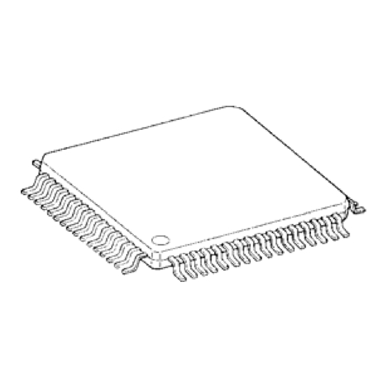
TB6560AHQ/AFG Package Dimensions Weight: 9.86 g (typ.) 2007-05-24 V1.0.3... - Page 31 TB6560AHQ/AFG Package Dimensions Weight: 0.26 g (typ.) Note: The rear heat sink block will be 5.5 mm × 5.5 mm. (PROVISIONAL) 2007-05-24 V1.0.3...
- Page 32 It is the responsibility of the buyer, when utilizing TOSHIBA products, to comply with the standards of safety in making a safe design for the entire system, and to avoid situations in which a malfunction or failure of such TOSHIBA products could cause loss of human life, bodily injury or damage to property.
Need help?
Do you have a question about the Preliminary TB6560AHQ and is the answer not in the manual?
Questions and answers