Hytera PNC370 Service Manual
Smart lte terminal
Hide thumbs
Also See for PNC370:
- User manual (22 pages) ,
- Operating instructions (2 pages) ,
- Quick reference manual (6 pages)
Table of Contents
Advertisement
Advertisement
Table of Contents

Related Manuals for Hytera PNC370


Summary of Contents for Hytera PNC370
- Page 1 PNC370 Smart LTE Terminal...
- Page 2 This manual describes the information related to the product repair. It is intended for use by qualified technicians only. To repair the product properly, please read this manual carefully before repairing. This manual is applicable to the following product: PNC370 PoC Terminal...
- Page 3 Copyright Information Hytera is the trademark or registered trademark of Hytera Communications Corporation Limited (the Company) in the People's Republic of China (PRC) and/or other countries or areas. The Company retains the ownership of its trademarks and product names. All other trademarks and/or product names that may be used in this manual are properties of their respective owners.
- Page 4 Documentation Information Conventions Instructional Conventions Icon Description Indicates information that can help you make better use of your product. Indicates references that can further describe the related topics. Indicates situations that could cause data loss or equipment damage. Indicates situations that could cause minor personal injury. Indicates situations that could cause major personal injury or even death.
-
Page 5: Table Of Contents
Service Manual Contents Contents 1. Product Layout ............................1 2. Disassembly and Reassembly ......................2 2.1 Tools ..............................2 2.2 Procedures ............................2 3. Exploded View and Packaging Guide ....................4 3.1 Exploded View ........................... 4 3.2 Packaging Guide ..........................6 4. - Page 6 Contents Service Manual 8.1 Installing Driver ..........................22 8.2 Upgrading Software ......................... 22 8.2.1 Preparation ..........................22 8.2.2 Procedure ..........................22 8.3 Testing the Radio ..........................24 8.3.1 Preparation ..........................24 8.3.2 Procedure ..........................24 8.3.3 Judgement Standard for Test Items ..................25 8.3.4 Hiding the Test App ........................
-
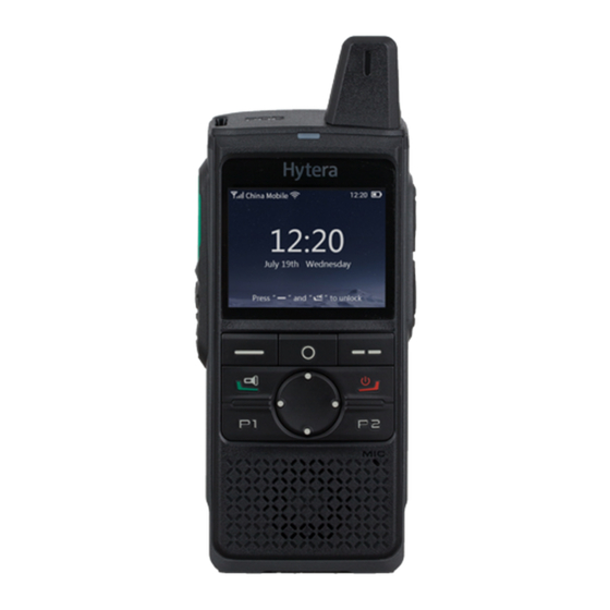
Page 7: Product Layout
Service Manual Product Layout 1. Product Layout... -
Page 8: Disassembly And Reassembly
Disassembly and Reassembly Service Manual 2. Disassembly and Reassembly This chapter describes how to disassemble the radio. To reassemble the radio, do vice versa. When reassembling the terminal, make sure that the waterproof ring is evenly inserted into the original position to ensure the waterproof performance of the terminal. 2.1 Tools Phillips screwdriver ... - Page 9 Service Manual Disassembly and Reassembly a. Use a T8 screwdriver to remove the four screws on the chassis. b. Use a tweezer to remove the FPC connector between the chassis and main board. c. Remove the chassis. Remove the main board as follows: a.
-
Page 10: Exploded View And Packaging Guide
Exploded View and Packaging Guide Service Manual 3. Exploded View and Packaging Guide 3.1 Exploded View The table below lists the parts. Part No. Description Part No. Description Protective film for Preloaded foam for 5113010000352A 5113050000345A lens battery cover 5110990000021A Light guide 5116000000243A Battery Latch 5116000002477A LED Cover... - Page 11 Service Manual Exploded View and Packaging Guide Part No. Description Part No. Description 5116000001101A Convex lens 51020200000053 Microphone Grounded 5115020000048A conductive foam for 5110000000033A Silicone MIC cover PC plate for 5113010000351A 5113030000026A Waterproof MIC mesh earpiece jack Silicone rubber 5110010000019A cover for battery 5111000002116A Left charging piece...
-
Page 12: Packaging Guide
Exploded View and Packaging Guide Service Manual 3.2 Packaging Guide... -
Page 13: Specifications
Service Manual Specifications 4. Specifications General Operating system Android 5.1 Qualcomm MSM8909, 1.1 GHz Storage 4 GB ROM and 512 MB RAM Dimensions (H x W x D) (with standard 121 mm x 55.5 mm x 24 mm battery) Weight (with standard battery) 185 g Size: 2.0 inch ... - Page 14 Specifications Service Manual GSM 900/1800 MHz TD-SCDMA B34/B39 CDMA BC0 Frequency Band WCDMA B1/B8 TDD-LTE B38/B39/B40/B41 FDD-LTE B1/B3/B5/B8 LTE Protocol 3GPP Speed Class CAT4 Wireless Module BT4.1 WLAN 2.4 GHz, 802.11 b/g/n Positioning System GPS,GLONASS,BDS Tracking sensitivity: <...
-
Page 15: Circuit Description
Service Manual Circuit Description 5. Circuit Description 5.1 Baseband Section 5.1.1 Control Module Power Supply Module VPH_PWR Charger LC network RFFE External connector Input power regulators management transceivers Input power management Modem IC, Fuel guage peripherals SMPS circuits LC network Audio LC network Display... - Page 16 Circuit Description Service Manual External Memory 1.2V 1.8V LDO5 VCCQ 2.9V LDO8 VREF_LPDDR VDDPX_3 eMMC RST_N MSM_RESOUT_N VDDPX_7 SDC1_CMD RCLK SDC1_RCLK SDC1_CLK SDC1_DATA[7:0] DAT[7:0] VDD1 VDD2 VDDQ VDDCA VREFCA/VREFDQ EBI0_CS_N0/1 CS0_N/CS1_N EBI0_CKE_0/1 CKE0/CKE1 LPDDR3 EBI0_DM[3:0] DM[3:0] EBI0_DQS[3:0] DQS_T[3:0] EBI0_DQSB[3:0] DQS_C[3:0] EBI0_CK/CKB CLK_T,CLK_C EBI0_CA[9:0]...
-
Page 17: Audio And Peripheral Module
Service Manual Circuit Description Display MIPI AP is connected to LCD (a 2.0-inch screen with resolution of 320 x 240) through MIPI. 5.1.2 Audio and Peripheral Module Audio Module The audio module consists of PMU and PA. The built-in CODEC of the PMU converses and processes the voice and digital signal. -
Page 18: Rf Section
Circuit Description Service Manual 5.2 RF Section V RE G_L_1P8 RFFE 5_CLK V BA T PM8909 RFFE 5_DAT A V RE G_L18_2P7 MSM8909 RFFE 1_CLK RFFE 1_DAT A A NT _1 A NT B41(38 DRX_LB1 DRX_LB2 orB7 DRX_LB3 DRX_MB 1 B1/3 1900 DRX_MB 2... -
Page 19: Main Receiving Circuit
Service Manual Circuit Description TDD TX Circuit The original TDD RF signal transmitted by the Transceiver goes to the PA for amplification, and then to the Filter for filtering. Afterwards, the filtered signal goes to the PA, switches to the ANT port, and then to the antenna unit. - Page 20 Circuit Description Service Manual post-filter to the RF Transceiver for demodulation. The WLAN/BT signal goes to the Switch through the GNSS/WLAN/BT three-in-one antenna, and then passes through the filter to the WLAN module for demodulation. At the same time, the WLAN/BT signal can be modulated in the WLAN module, and then passes through the filter and the Switch to the GNSS/WLAN/BT three-in-one antenna for transmission.
-
Page 21: Circuit Inspection
Service Manual Circuit Inspection 6. Circuit Inspection 6.1 Baseband Section 6.1.1 Downloading Failed You cannot download. Check the installation of Check whether the driver. port can be Check the data cable for detected. downloading. Replace the main board. 6.1.2 Powering On Failed You cannot power on the radio. -
Page 22: Lighting Up Screen Failed
Circuit Inspection Service Manual 6.1.3 Lighting Up Screen Failed You cannot light up the screen. Dissemble the Properly connect terminal to check the display whether the display connector. connector is properly connected. Replace the display Replace the to check whether it main board. -
Page 23: Turning On Backlight/Flashlight Failed
Service Manual Circuit Inspection 6.1.5 Turning On Backlight/Flashlight Failed You cannot turn on the backlight or flashlight. Dissemble the terminal to check Properly connect whether their FPC the FPC connectors are connectors. properly connected. Replace the FPC connectors to check Replace the whether the backlight main board. -
Page 24: Keypad Failed To Respond
Circuit Inspection Service Manual 6.1.7 Keypad Failed to Respond The keypad makes no response to the key operations. Check whether the Properly keypad FPC is connect the properly keypad FPC. connected. Replace the keypad to check Replace the whether it can main board. -
Page 25: Rf Section
Service Manual Circuit Inspection 6.2 RF Section 6.2.1 Calibration Totally Failed Detect whether short circuit exists in the power-on current, and high current exists in the power-off mode. Check whether the port in the Device Manager on the computer is normal. Check whether it is properly soldered from the antenna switch to test socket. -
Page 26: Wi-Fi Section
Circuit Inspection Service Manual 6.3 Wi-Fi Section 6.3.1 Connecting to Wi-Fi Networks Failed You cannot activate Wi-Fi. Based on the schematic diagram, Check whether the power check whether the has short circuit, and then output voltage of re-solder or replace U1400. U1400 is normal. -
Page 27: Interface Details
Service Manual Interface Details 7. Interface Details Interface Pin No. Signal VBUS USB_DM USB connector USB_DP USB_HS_ID SPK+ Audio connector MIC+ 1, 6 VREG_L14_UIM1 UIM1_RESET UIM1_CLK SIM card Interface 4, 8 UIM1_DATA... -
Page 28: Tuning Description
Tuning Description Service Manual 8. Tuning Description All software and tools are available in the software package published by the Company. 8.1 Installing Driver When the terminal is successfully connected to PC through the USB cable, the PC Device Manager displays the port of Diagnostic and ADB. - Page 29 Service Manual Tuning Description Select the rawprogram0.xml file to download. (If you find no such file, consult the relevant R&D or technical support engineer.) Click Start. The Download Info panel displays PASS when the burning is completed.
-
Page 30: Testing The Radio
Restart the terminal. 8.3 Testing the Radio 8.3.1 Preparation You have prepared the following devices: the terminal of PNC370, battery, USB cable, SIM card, earpiece, desktop charger, WIFI network, and BT device. 8.3.2 Procedure Power on the radio with the SIM card inserted. -
Page 31: Judgement Standard For Test Items
Service Manual Tuning Description Select Factory test. (If Factory test does not appear on the interface, run the open test file to make it show up. If the screen turns to black and white when power-on, the terminal enters the FFBM mode.) Press the P1 key, and then the automatic test starts from the first item to the last one (15 test items in total). -
Page 32: Hiding The Test App
Tuning Description Service Manual Test Item Operation & Judgement Standard Note the recorded file. Test the rear microphone. Second Press the P1 key to start recording. Key test item. PhoneLoopback test Press the P1 key again to start playing the recorded file. Insert the earpiece, and then press the PTT key to speak into the earpiece MIC. -
Page 33: Block Diagram
Service Manual Block Diagram 9. Block Diagram 9.1 Baseband Section MIC1 MIC2 TORCH 3.3V BL Earpiece SPK- SPK+ Keypad&LED Audio PA (MSM8909) Indiate LED gpio VOL/PTT key Micro USB TCXO EMMC (PM8909) (4+4DDR3) Desktop charger... -
Page 34: Rf Section
Block Diagram Service Manual 9.2 RF Section V RE G_L_1P8 RFFE 5_CLK V BA T PM8909 RFFE 5_DAT A V RE G_L18_2P7 MSM8909 RFFE 1_CLK RFFE 1_DAT A A NT _1 A NT B41(38 DRX_LB1 DRX_LB2 orB7 DRX_LB3 DRX_MB 1 B1/3 1900 DRX_MB 2... -
Page 35: Part List
Service Manual Part List 10. Part List Ref No. Part No. Priority Description X0000002268 Mechanical material for radio unit 5116000002471A Chassis 50151100000040 Optional Antenna 5116000000841A Micro USB cover 5116000001582A Accessory connector cover 5116000001552A Stopper for accessory connector cover 5110000000033A Silicone rubber cover for microphone 51020200000053 Optional Microphone... - Page 36 Part List Service Manual Ref No. Part No. Priority Description connector 5110030000050A Waterproof ring 5115020000047A Grounded conductive foam for key 50100200000057 Optional TFT LCD 5113070000151A Double-sided tape for LENS 5116000002578B LCD lens 11510000062236 Front case processing component 5116000002470A Front housing 1.01 5116000002472A PTT key bracket...
- Page 37 Service Manual Part List Ref No. Part No. Priority Description 50050800000051 Optional ESD protection diode CON1 51040100000261 Optional Board-to-board connector 5001020000539C 11500000004819 Semi-finished keypad 50020100001205 Optimized Chip capacitor D1, D2, D3, 50050600000125 Optional D4, D5 51040100000058 Optimized Board-to-board connector 50070300000055 Optional N-MOSFET 50030100001917...
- Page 38 Part List Service Manual Ref No. Part No. Priority Description 50099900000006 B4 main board for China B5 (FDD-LTE: B1/B3/B5/B7/B8/B20) 54991010002080 MEIG main board 54991010002840 B6 main board for Americas...
- Page 39 Hytera Communications Corporation Limited. 2019 Hytera Communications Corporation Limited. All Rights Reserved. Address: Hytera Tower, Hi-Tech Industrial Park North, 9108# Beihuan Road, Nanshan District, Shenzhen, People's Republic of China Postcode: 518057 http:// www.hytera.com...
Need help?
Do you have a question about the PNC370 and is the answer not in the manual?
Questions and answers