Table of Contents
Advertisement
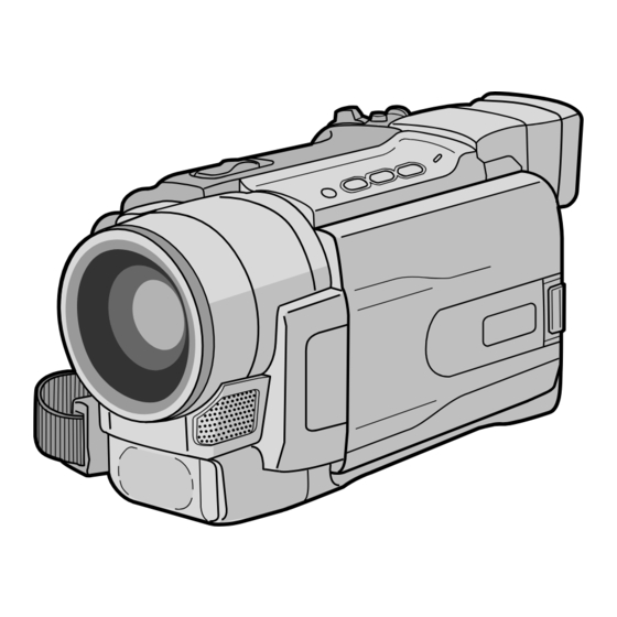
SERVICE MANUAL
GR-DVL365EG/EK,DVL367EG/EK,DVL567EG
Regarding service information other than these sections, refer to the GR-DVL167EG service manual (No. 86662).
Also, be sure to note important safety precautions provided in the service manual.
SPECIFICATIONS
(The specifications shown pertain specifically to the model GR-DVL160,167,365,367,567,765,767,865,867)
Power supply
: DC 11.0 V
DC 7.2 V
Power consumption
LCD monitor off, viewfinder on : Approx. 4.5 W (GR-DVL867/DVL865/DVL767/DVL765)
Approx. 4.3 W (GR-DVL567/DVL367/DVL365/DVL167/DVL160)
LCD monitor on, viewfinder off : Approx. 5.7 W (GR-DVL867/DVL865/DVL767/DVL765)
Approx. 5.3 W (GR-DVL567/DVL367/DVL365/DVL167/DVL160)
Video light
: Approx. 2.8 W (GR-DVL867/DVL865/DVL767/DVL765)
Approx. 3.5 W (GR-DVL567/DVL367/DVL365/DVL167/DVL160)
Dimensions (W x H x D)
: 79 mm x 89 mm x 184 mm (GR-DVL867/DVL865/DVL767/DVL765)
79 mm x 89 mm x 167 mm (GR-DVL567/DVL367/DVL365/DVL167/DVL160)
(with the LCD monitor closed and the viewfinder pushed down)
Weight
: Approx. 580 g (GR-DVL867/DVL865)
Approx. 570 g (GR-DVL767/DVL765/DVL567)
Approx. 560 g (GR-DVL367/DVL365)
Approx. 550 g (GR-DVL167/DVL160)
Operating temperature
: 0°C to 40°C
Operating humidity
: 35% to 80%
Storage temperature
: –20°C to 50°C
Pickup
: 1/3.8" CCD (GR-DVL867/DVL865/DVL767/DVL765)
1/4" CCD (GR-DVL567/DVL367/DVL365/DVL167/DVL160)
Lens
: F 1.8, f = 3.8 mm to 38 mm, 10:1 power zoom lens
(GR-DVL867/DVL865/DVL767/DVL765)
F 1.8, f = 3.6 mm to 36 mm, 10:1 power zoom lens
(GR-DVL567/DVL367/DVL365/DVL167/DVL160)
Filter diameter
: ø37 mm
LCD monitor
: 3.5" diagonally measured, LCD panel/TFT active matrix system
(GR-DVL867/DVL865/DVL567)
2.5" diagonally measured, LCD panel/TFT active matrix system
(GR-DVL767/DVL765/DVL367/DVL365/DVL167/DVL160)
Viewfinder
: Electronic viewfinder with 0.24" black/white LCD
Speaker
: Monaural
Digital Video Camera
Format
: DV format (SD mode)
Signal format
: PAL standard
Recording/Playback format : Video: Digital component recording
: Audio: PCM digital recording, 32 kHz 4-channel (12-bit), 48 kHz 2-channel (16-bit)
Cassette
: Mini DV cassette
Tape speed
: SP: 18.8 mm/s
LP: 12.5 mm/s
Maximum recording time
: SP: 80 min.
(using 80 min. cassette)
LP: 120 min.
DIGITAL VIDEO CAMERA
Camcorder
General
(Using AC Adapter)
(Using battery pack)
This service manual is printed on 100% recycled paper.
COPYRIGHT © 2002 VICTOR COMPANY OF JAPAN, LTD.
Digital Still Camera Function (GR-DVL867/DVL865/DVL767/DVL765/DVL567/DVL367/DVL365 only)
Storage media
: SD Memory Card/MultiMediaCard
Compression system
: Still image : JPEG (compatible)
Moving image : MPEG4 (compatible)
File size
: 3 modes (1280 X 960 pixels*, 1024 x 768 pixels,
640 x 480 pixels)
Picture quality
: 2 modes (FINE/STANDARD)
Approximate number of
storable images
:
pg. 27.
* GR-DVL867/DVL865/DVL767/DVL765 only.
Connectors
S-Video
: Y:1 V (p-p), 75 Ω, analogue
Output
C:0.29 V (p-p), 75 Ω, analogue
AV
: 1 V (p-p), 75 Ω, analogue
Video output
Audio output
: 300 mV (rms), 1 kΩ, analogue, stereo
DV
Output
: 4-pin, IEEE 1394 compliant
Input (GR-DVL867/DVL767/
: 4-pin, IEEE 1394 compliant
DVL567/DVL367/DVL167 only)
USB (GR-DVL867/DVL865/
DVL767/DVL765/DVL567/
DVL367/DVL365 only)
: 5-pin
PC (GR-DVL167/DVL160 only)
: ø2.5 mm, 3-pole
EDIT (GR-DVL867/DVL865/
DVL767/DVL765/DVL567/
DVL367/DVL365 only)
: ø3.5 mm, 2-pole
JLIP (GR-DVL167/DVL160 only) : ø3.5 mm, 4-pole
AC Adapter
Power requirement
: AC 110 V to 240 V`, 50 Hz/60 Hz
Output
: DC 11 V
Specifications shown are for SP mode unless otherwise indicated.
E & O.E. Design and specifications subject to change without notice.
, 1 A
No. 86667
February 2002
Advertisement
Chapters
Table of Contents


Need help?
Do you have a question about the GR-DVL365EG and is the answer not in the manual?
Questions and answers