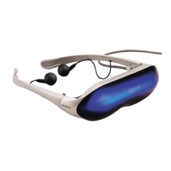
Sony Glasstron Lite PLM-A35E Service Manual
Hide thumbs
Also See for Glasstron Lite PLM-A35E:
- Operating instructions manual (76 pages) ,
- Operating instructions manual (32 pages)
Table of Contents
Advertisement
Quick Links
SERVICE MANUAL
Power supply
AC power adaptor: AC-PLM2
100-240 V AC, 50/60 Hz, 16 W
Output voltage 9 V, 1.3 A
Battery pack: NP-F550 (not supplied)
Power consumption
1.8 W Approx.
Operating temperature
5°C to 35°C (41°F to 95°F)
Storage temperature
–10°C to 60°C (14°F to 140°F)
Dimensions
Display unit:
Approx. 173 × 53 × 56 mm
(Approx. 6
(w/h/d, folded up)
Power supply box:
Approx. 53 × 39 × 104 mm
(Approx. 2
(w/h/d)
not including projecting parts and
controls
Mass
Display unit: Approx. 100 g (4 oz)
Power supply box: Approx. 90 g (3.2 oz)
Video signal
PAL colour, EIA standards
9-928-144-11
SPECIFICATIONS
× 2
× 2
7
1
1
/
/
/
inches)
8
8
4
× 1
× 4
1
/
9
/
1
/
inches)
8
16
8
PLM-A35E
Audio/video input
Special minijack
1 Vp-p, 75 ohms, unbalanced, sync
negative
S video input
4-pin mini DIN
Y: 1 Vp-p, 75 ohms, unbalanced, sync
negative
C: 0.286 Vp-p, 75 ohms, unbalanced, sync
negative
Supplied accessories
AC power adaptor AC-PLM2 (1)
Mains lead (1)
Audio/video cable (special miniplug y
phono plug) (3 m) (1)
Audio/video cable (special miniplug y
stereo miniplug) (0.5 m) (1)
Plug adaptors
(phono jack y phono jack) (3)
Nose piece (black) (1)
Side piece pads (2)
Operating instructions manual (1)
Safety Instructions (1)
Warranty (1)
Design and specifications are subject to
change without notice.
AEP Model
GLASSTRON
Advertisement
Table of Contents

Related Manuals for Sony Glasstron Lite PLM-A35E


Summary of Contents for Sony Glasstron Lite PLM-A35E
- Page 1 PLM-A35E SERVICE MANUAL AEP Model SPECIFICATIONS Power supply Audio/video input Special minijack AC power adaptor: AC-PLM2 1 Vp-p, 75 ohms, unbalanced, sync 100-240 V AC, 50/60 Hz, 16 W Output voltage 9 V, 1.3 A negative Battery pack: NP-F550 (not supplied) S video input Power consumption 4-pin mini DIN...
-
Page 2: Table Of Contents
LINE WITH MARK 0 ON THE SCHEMATIC DIAGRAMS AND IN THE PARTS LIST ARE CRITICAL TO SAFE OPERATION. REPLACE THESE COMPONENTS WITH SONY PARTS WHOSE PART NUMBERS APPEAR AS SHOWN IN THIS MANUAL OR IN SUPPLEMENTS PUB- LISHED BY SONY. -
Page 3: General
Caution: The screen is always right in front of you. Congratulations on your purchase of a Sony Note on the LCD (Liquid Crystal The Glasstron is a face-mounted display. With this type of display, the screen is always in front Glasstron Personal Viewer. -
Page 4: Wearing The Glasstron
(phono jacks) of your video carried to the Glasstron depending on the equipment, connect the Glasstron to both the video source. In this case, contact your Sony right and left audio output jacks. If you dealer or local authorized Sony service connect the Glasstron to just one audio output facility. -
Page 5: Using The Glasstron
If you cannot see a proper arrangement of these lines even after resting your eyes for a few hours, the Glasstron may not be operating correctly. Contact your Sony dealer or local authorized Sony service facility. continued... -
Page 6: Setting The User Lock
NP-F530/F730/F750/F930/F950 (not characteristic. supplied) with the Glasstron. * You can use an “InfoLITHIUM ™ ” battery “InfoLITHIUM” is a trademark of Sony pack with the Glasstron. When using such a Corporation. battery pack, the estimated remaining battery life is displayed with the indicator instead of the time counter. -
Page 7: Checking The Supplied Accessories
When the battery pack is weak, the Check that the following accessories are supplied with your Glasstron. If any item is not following message appears on the supplied, contact your Sony dealer or local authorized Sony service facility. battery life screen. Replace the battery pack with a charged one. - Page 8 MEMO Confidential PLM-A35E (AEP) (END)
-
Page 9: Disassembly
SECTION 2 DISASSEMBLY Note: Follow the disassembly procedure in the numerical order given. CABINET (FRONT) 2 two screws (PTT1.7 × 6) 4 three claws 2 two screws (PTT1.7 × 6) 3 screw (PTT1.7 × 6) 5 cabinet (front) RG-A01 (C) COMPLETE PWB, HP-A01 (C) MOUNTED PWB, DL-A01 COMPLETE PWB 6 unweaved cloth 8 screw 7 connector... - Page 10 BACK LIGHT UNIT 3 back light unit 3 back light unit 1 unweaved cloth 2 two claws 4 lens block 1 unweaved cloth 2 two claws EAR MDR-E805PT//K SET RECIVER (HP701, 702) qa vine (R) 7 two bosses 5 claw qs two ear MDR-E805PT//K SET recivers (HEADPHONE (L/R)) 9 two bosses...
-
Page 11: Electrical Adjustments
SECTION 3 ELECTRICAL ADJUSTMENTS Precautions on adjustment: 5. Setting up Input Signals 1. Perform the adjustment in the given order. (1) S VIDEO Signal 2. Power supply voltage: DC 9 V Connect an oscilloscope to the Y signal pin of the S VIDEO 3. - Page 12 [Preparation for Adjustment] • Adjustment data writing 1. Service Jigs The PAUSE button must be pressed to write adjustment (1) Adjusting remote commander (RM-95-modified) data (D page) to the nonvolatile memory (EEPROM). (Un- Note: J-6082-053-B less the PAUSE is pressed, new data are not saved in the (2) Extension cable (for remote commander plug converter) nonvolatile memory.) J-6082-291-A...
- Page 13 5. Data Processing Certain adjustment items require the microprocessor data to be read out or the displayed data (hexadecimal numbers) on jigs or adjusting remote commander to be calculated to get adjustment data. In such a case, convert hexadecimal numbers into decimal numbers once, then make calculation, and convert its result into hexadecimal number as adjustment data.
- Page 14 6. Power ON Procedure for Adjustment (1) Connect an extension cable to the adjusting remote commander. (2) After making sure that the HOLD switch on the adjusting remote commander is not turned on (not at left (NOR) position), supply 9 Vdc to the DC IN (J101).
- Page 15 [Preset Data Writing] Connection: (1) Connect the adjusting remote commander to the CN305 on YM-A01 board. Data Writing Procedure (1) Set data: 01 to page: 1, address: 00. (2) Enter the data given in the table below. Note: To write the data to the EEPROM, press the PAUSE button on the adjusting remote commander each time the data is set. (3) After writing all data, set data: 00 to page: 1, address: 00.
- Page 16 [Brightness Volume Center Adjustment] LCD BLOCK Preparation: • To adjust the LCD block, connect a pattern generator as shown [BRIGHT] control (RV301): Center (click position) below. (For details, see page 3-1) Condition: Pattern generator Input signal Color bar signal (white 75%) Measurement point Displayed data on the adjusting remote commander...
- Page 17 [G Contrast Adjustment] [G Brightness Adjustment] Condition: Condition: 10 step signal, 1 Vp-p 10 step signal, 1 Vp-p Input signal Input signal (White: 100%) (White: 100%) Measurement point RG-A01 board CN803 pin 2 Measurement point RG-A01 board CN803 pin 2 Measuring equipment Oscilloscope Measuring equipment...
- Page 18 [R Contrast Adjustment] [R Brightness Adjustment] Condition: Condition: 10 step signal, 1 Vp-p 10 step signal, 1 Vp-p Input signal Input signal (White: 100%) (White: 100%) Measurement point RG-A01 board CN803 pin 4 Measurement point RG-A01 board CN803 pin 4 Measuring equipment Oscilloscope Measuring equipment...
- Page 19 [B Contrast Adjustment] [B Brightness Adjustment] Condition: Condition: 10 step signal, 1 Vp-p 10 step signal, 1 Vp-p Input signal Input signal (White: 100%) (White:100%) Measurement point RG-A01 board CN803 pin 3 Measurement point RG-A01 board CN803 pin 3 Measuring equipment Oscilloscope Measuring equipment Oscilloscope...
- Page 20 [Color Adjustment] [Burst Cleaning Level Adjustment] Condition: Condition: Input signal Color bar signal (White: 75%) Input signal Anti-pal signal (Anti-pal signal is included in special color-bar signal and so on.) Measurement point RG-A01 board CN803 pin 2 Measurement point RG-A01 board CN803 pin 3 Measuring equipment Oscilloscope Measuring equipment...
- Page 21 [Burst Cleaning Phase Adjustment] Condition: Input signal Color bar signal Measurement point RG-A01 board CN803 pin 3 Measuring equipment Oscilloscope Adjustment part CT911 (DL-A01 board) Specified value Less than 50 mV Connection: Oscilloscope (DC range) RG-A01 Board CN803 pin 3 (B OUT) –...
- Page 22 [LED Back Light Brightness Balance Adjustment] OPTICS BLOCK • Make this adjustment through a visual check. • To adjust the optics block, connect a pattern generator as shown Condition: below. (For details, see page 3-1) Input signal White: 100% signal Measurement point LCD screen Pattern generator...
- Page 23 POWER SUPPLY BLOCK [Battery Down Adjustment] Connector for check (CN305) YM-A01 board Pattern Preparation: generator Adjusting [VOL] • control (RV201) : Maximum Remote A/V IN jack (J402) [AVLS] • switch (S201) : OFF Commander Audio YM-A01 board [BRIGHT] • control (RV301): Center (click position) Condition: VIDEO IN: Color bar Signal...
- Page 24 Adjustment and Connection Location: Connect adjusting remote commander – YM-A01 Board (Side A) – CN305 S VIDEO IN jack (J401) A/V IN Volume Brightness jack control control (J402) (RV201) (RV301) AVLS switch (S201) – DL-A01 Board (Side A) – – RG-A01 Board (Side B) – IC801 CT911 CN803...
-
Page 25: Diagrams
SECTION 4 DIAGRAMS 4-1. BLOCK DIAGRAM – AUDIO/VIDEO Section – (Page 4-3) CV/S VIDEO SELECT SWITCH, VIDEO AMP IC401 EXT VIDEO (ON: PLUG IN) SYNC LEVEL CLAMP BUFFER SHIFT Q402 IC407 IC405 (1/4) BUFFER H SYNC Q408 VIDEO SELECT SWITCH, J401 VIDEO AMP S VIDEO IN... -
Page 26: Block Diagram - Lcd Section
4-2. BLOCK DIAGRAM – LCD Section – LCD RGB DECODER, LCD DRIVE, LCD TIMING GENERATOR IC801 Y ATT Y BUFFER Y IN B OUT Q811 Q812 (Page 4-2) SYNC IN G OUT R OUT C ATT C BUFFER C IN Q813 Q814 HCK1... -
Page 27: Block Diagram - Key Control/Power Supply Section
4-3. BLOCK DIAGRAM – KEY CONTROL/POWER SUPPLY Section – SYSTEM CONTROLLER IC301 (2/2) DC IN DC IN NON DETECT SWITCH Q303 DC/DC CONVERTER T101 L101 D108 J101 D102 RIPPLE L106 SWITCHING F301 S101 AUDIO CIRCUIT FILTER REGULATOR (POWER SWITCH) DC IN 9V Q203 Q102 D101... -
Page 28: Note For Printed Wiring Boards And Schematic Diagrams
4-4. NOTE FOR PRINTED WIRING BOARDS AND SCHEMATIC DIAGRAMS • Circuit Boards Location Note on Printed Wiring Board: Note on Schematic Diagram: • X : parts extracted from the component side. • All capacitors are in µF unless otherwise noted. pF: µµF •... -
Page 29: Printed Wiring Board - Ym-A01 Board
4-5. PRINTED WIRING BOARD – YM-A01 Board – • Semiconductor Location (Side A) Ref. No. Location D307 D316 D410 D411 IC302 IC303 (Page 4-19) IC304 Q203 Q304 (Page 4-30) • Semiconductor Location (Side B) Ref. No. Location D311 D401 D402 D403 D404 D405... - Page 30 4-6. SCHEMATIC DIAGRAM – YM-A01 Board (1/2) – • • See page 4-33 for Waveforms. See page 4-36 for IC Block Diagrams. (Page 4-13) (Page 4-13) (Page 4-13) (Page 4-15) (Page 4-15) (Page 4-13) (Page 4-15) (Page 4-13) Confidential PLM-A35E (AEP) 4-11 4-12...
-
Page 31: Schematic Diagram - Ym-A01 Board (1/2)
4-7. SCHEMATIC DIAGRAM – YM-A01 Board (2/2) – • See page 4-33 for Waveforms. • See page 4-36 for IC Block Diagram. (Page 4-12) (Page 4-16) (Page 4-12) (Page 4-11) (Page 4-11) (Page 4-32) (Page 4-11) (Page 4-12) (Page 4-27) (Page 4-16) (Page 4-12) (Page 4-11) -
Page 32: Schematic Diagram - Rg-A01 Board
4-8. SCHEMATIC DIAGRAM – RG-A01 Board – • See page 4-33 for Waveforms. • See page 4-38 for IC Block Diagrams. (Page 4-13) (Page 4-13) (Page 4-27) (Page 4-23) Confidential PLM-A35E (AEP) 4-16 4-17 4-18... - Page 33 4-9. PRINTED WIRING BOARD – RG-A01 Board – • See page 4-8 for Circuit Boards Location. (Page 4-9) • Semiconductor Location (Side A) Ref. No. Location D801 IC804 Q811 Q812 Q813 Q814 (Page 4-9) Q830 Q831 Q901 DL-A01 BOARD CN911 (Page 4-25) (Page 4-22) •...
-
Page 34: Printed Wiring Board - Dl-A01 Board
4-10. PRINTED WIRING BOARD – DL-A01 Board – • See page 4-8 for Circuit Boards Location. (Page 4-19) • Semiconductor • Semiconductor Location Location (Side A) (Side B) Ref. No. Location Ref. No. Location Q912 IC911 Q914 Q915 Q911 Q913 Confidential PLM-A35E (AEP) 4-21... -
Page 35: Schematic Diagram - Dl-A01 Board
4-11. SCHEMATIC DIAGRAM – DL-A01 Board – • See page 4-34 for Waveforms. • See page 4-39 for IC Block Diagram. (Page 4-16) Confidential 4-23 4-24 PLM-A35E (AEP) -
Page 36: Printed Wiring Board - Hp-A01 Board
4-12. PRINTED WIRING BOARD – HP-A01 Board – • See page 4-8 for Circuit Boards Location. (Page 4-9) (Page 4-19) • Semiconductor Location (Side B) Ref. No. Location Ref. No. Location D702 Q704 D703 Q705 D704 Q706 D705 Q707 Q708 Q701 Q709 Q710... -
Page 37: Schematic Diagram - Hp-A01 Board
4-13. SCHEMATIC DIAGRAM – HP-A01 Board – (Page 4-13) (Page 4-18) Confidential 4-27 4-28 PLM-A35E (AEP) - Page 38 4-14. PRINTED WIRING BOARD – DD-A02 Board – • See page 4-8 for Circuit Boards Location. (Page 4-9) • Semiconductor Location (Side B) Ref. No. Location D101 D102 D103 D104 D108 IC101 IC102 Q101 Q102 Q103 Q104 Q105 Confidential PLM-A35E (AEP) 4-29 4-30...
-
Page 39: Schematic Diagram - Dd-A02 Board
4-15. SCHEMATIC DIAGRAM – DD-A02 Board – • See page 4-35 for Waveforms. • See page 4-40 for IC Block Diagram. (Page 4-13) Note: The components identified by mark 0 or dotted line with mark 0 are critical for safety. Replace only with part number specified. - Page 40 • Waveforms – YM-A01 Board – – DL-A01 Board – – RG-A01 Board – 6 IC801 ta VXO IN qa IC801 tl YIN 1 FL401 3, 4 6 IC301 <z// CL0 1 Q811 Base 1 IC911 1 IN 416 mVp-p 840 mVp-p 408 mVp-p 688 mVp-p...
- Page 41 – DD-A02 Board – 6 IC101 rk CB1 1 IC101 1 CA1 4.2 Vp-p 2.8 Vp-p 3.3 µs 3.3 µs 2 IC101 qj CT 7 Q102 Collector 18 Vp-p 624 mVp-p 3.3 µs 3.3 µs 3 IC101 ek VE4 8 Q102 Base 760 mVp-p 84 mVp-p 3.3 µs...
- Page 42 • IC Block Diagrams – YM-A01 Board – IC201 BA3574BFS-E2 MUTE SW 11 MUTE MUTE BB SW MUTE SW PW SW 12 P.SW AVC DET IN 1 13 AVC IN MIX OUT IN 2 14 OUT 1 BIAS OUT 15 BIAS IN 16 RF OUT 17 VREF...
- Page 43 IC401, 402 MM1113XFBE BUFFER BIAS IC404 MSM5258MS-KR1 RESET V. DECODER PAL/NTSC COMP. SYNC 1/525, 1/625 1/19 V. COUNTER H. COUNTER Confidential 4-37 PLM-A35E (AEP)
- Page 44 – RG-A01 Board – IC801 CXA3017R-T6 +12V +12V VCC1 DA OUT BLKLIM WHTLIM VXO OUT 50 POL SW INT/EXT VXO IN 51 PSIG- PSIG-BRT PAL ID POL SW BRIGHT COLOR DEMOD EXT COLOR VGATE APC 52 WIDE VJOG & BALANCE PALSW R-BRT SUB-...
- Page 45 IC804 M62367GP-75ED – – 12BIT SHIFT RESISTOR 8BIT 8BIT R-2R+SEGMENT R-2R+SEGMENT D/A CONVERTER D/A CONVERTER 8BIT ADDRESS 8BIT LATCH DECODER LATCH 8BIT 8BIT 8BIT 8BIT 8BIT 8BIT LATCH LATCH LATCH LATCH LATCH LATCH 8BIT 8BIT 8BIT 8BIT 8BIT 8BIT R-2R+SEGMENT R-2R+SEGMENT R-2R+SEGMENT R-2R+SEGMENT...
- Page 46 – DD-A02 Board – IC101 MB3785APFV-G-BND-ER 36 35 34 33 32 31 30 28 27 26 25 –IN 3 (C) CB 4 CTL 3 VE 4 CTL 2 OUT 4 CTL 1 +2.5V OUT 3 VOLTAGE VREF REFERENCE VE 3 VE 2 XTAL OSCO...
-
Page 47: Ic Pin Function Description
4-16. IC PIN FUNCTION DESCRIPTION • YM-A01 BOARD IC301 MB89082PFV-G-118-BND (SYSTEM CONTROLLER) Pin No. Pin Name Description TEST MODE 0 Setting terminal for the test mode (Normally: fixed at “L”) TEST MODE 1 Setting terminal for the test mode (Normally: fixed at “L”) Main system clock input terminal (10MHz) Main system clock output terminal (10MHz) —... - Page 48 Pin No. Pin Name Description — Ground terminal SEG07 to SEG00 57 to 64 LCD segment drive signal output terminal Not used (open) V3 to V0 65 to 68 Bias voltage input for the LCD drive Not used COM0 to COM3 69 to 72 LCD common drive signal output terminal Not used (open) SYNC DET...
- Page 49 • RG-A01 BOARD IC801 CXA3017R-T6 (LCD RGB DECODER, LCD DRIVE, LCD TIMING GENERATOR) Pin No. Pin Name Description EXT R External digital R signal input terminal Not used (fixed at “L”) EXT G External digital G signal input terminal Not used (fixed at “L”) EXT B External digital B signal input terminal Not used (fixed at “L”) TRAP...
- Page 50 Pin No. Pin Name Description G OUT G signal (primary color signal) output to the left and right LCD units FB G Capacitor connection terminal for DC voltage feedback circuit of G signal (pin rd) R OUT R signal (primary color signal) output to the left and right LCD units FB R Capacitor connection terminal for DC voltage feedback circuit of R signal (pin rg) —...
-
Page 51: Exploded Views
SECTION 5 EXPLODED VIEWS NOTE: • -XX and -X mean standardized parts, so they • Items marked “*” are not stocked since they are seldom required for routine service. Some may have some difference from the original one. delay should be anticipated when ordering •... - Page 52 (2) CABINET SECTION-2 not supplied CONNECTION CORD Ref. No. Part No. Description Remark Ref. No. Part No. Description Remark 4-644-739-01 BEARING (L), HINGE 4-644-735-02 VINE (L) 4-644-704-02 SPRING, NOSE 3-929-548-11 SCREW (1.7X6), +PTT 4-644-705-01 BLOCK, NOSE 4-644-737-02 BLOCK (L), HINGE 4-644-738-01 BEARING (R), HINGE 4-645-477-01 SHEET, HINGE BLIND X-4622-756-1 CABINET (REAR) ASSY...
- Page 53 (3) IF-BOX BLOCK SECTION supplied not supplied supplied supplied supplied not supplied Ref. No. Part No. Description Remark Ref. No. Part No. Description Remark 4-644-715-01 COVER, BATTERY 1-791-933-11 CORD, CONNECTION (MR) X-4622-740-1 CABINET (IF) ASSY, UPPER 1-791-934-11 CABLE, FLAT (FFC) 17P 3-988-786-11 BUTTON, BATTERY RELEASE 3-948-339-61 TAPPING 3-050-073-11 KNOB, POWER...
- Page 54 MEMO Confidential PLM-A35E (AEP) (END) (END)
-
Page 55: Electrical Parts List
SECTION 6 DD-A02 ELECTRICAL PARTS LIST NOTE: • Due to standardization, replacements in the • Items marked “*” are not stocked since they The components identified by mark 0 or dotted line with mark parts list may be different from the parts speci- are seldom required for routine service. - Page 56 DD-A02 DL-A01 HP-A01 Ref. No. Part No. Description Remark Ref. No. Part No. Description Remark R111 1-218-871-11 METAL CHIP 0.5% 1/16W R112 1-218-871-11 METAL CHIP 0.5% 1/16W CT911 1-141-367-51 CAP, CHIP TRIMMER 20PF R113 1-218-903-11 METAL CHIP 220K 0.5% 1/16W R114 1-218-863-11 METAL CHIP 4.7K...
- Page 57 HP-A01 RG-A01 Ref. No. Part No. Description Remark Ref. No. Part No. Description Remark Q708 8-729-402-38 TRANSISTOR 2SD1819A-R-TX Q709 8-729-402-38 TRANSISTOR 2SD1819A-R-TX C821 1-162-964-11 CERAMIC CHIP 0.001uF Q710 8-729-402-38 TRANSISTOR 2SD1819A-R-TX C822 1-110-501-11 CERAMIC CHIP 0.33uF C823 1-162-970-11 CERAMIC CHIP 0.01uF R701 1-216-864-11 SHORT...
- Page 58 RG-A01 YM-A01 Ref. No. Part No. Description Remark Ref. No. Part No. Description Remark C210 1-164-489-11 CERAMIC CHIP 0.22uF R823 1-216-864-11 SHORT C211 1-164-390-91 CERAMIC CHIP 330PF R824 1-216-864-11 SHORT R825 1-216-833-91 RES-CHIP 1/16W C212 1-164-390-91 CERAMIC CHIP 330PF R826 1-216-834-11 RES-CHIP 1/16W C214...
- Page 59 YM-A01 Ref. No. Part No. Description Remark Ref. No. Part No. Description Remark C346 1-162-921-11 CERAMIC CHIP 33PF FB403 1-216-864-11 SHORT C402 1-124-778-21 ELECT CHIP 22uF 6.3V FB404 1-216-864-11 SHORT C403 1-164-156-11 CERAMIC CHIP 0.1uF FB405 1-216-864-11 SHORT C404 1-124-778-21 ELECT CHIP 22uF 6.3V C405...
- Page 60 YM-A01 Ref. No. Part No. Description Remark Ref. No. Part No. Description Remark R220 1-216-864-11 SHORT R357 1-216-845-11 RES-CHIP 100K 1/16W R221 1-216-789-11 RES-CHIP 1/16W R222 1-216-789-11 RES-CHIP 1/16W R361 1-216-838-11 RES-CHIP 1/16W R223 1-216-864-11 SHORT R362 1-216-831-11 RES-CHIP 6.8K 1/16W R363 1-216-821-11 RES-CHIP...
- Page 61 YM-A01 Ref. No. Part No. Description Remark Ref. No. Part No. Description Remark XTL301 1-579-369-21 VIBRATOR (10MHz) ************************************************************** ACCESSORIES & PACKING MATERIALS ******************************* 1-475-456-24 ADAPTOR, AC (AC-PLM2) 1-575-131-31 CORD, POWER 1-777-690-11 CORD, CONNECTION 1-782-711-11 CABLE, AV MONITOR 3-868-186-31 MANUAL, INSTRUCTION (ENGLISH, FRENCH, GERMAN) 3-868-186-41 MANUAL, INSTRUCTION (DUTCH, SPANISH, ITALIAN)
- Page 62 PLM-A35E (AEP) This manual and the constituent data may not be replicated, copied nor reprinted in whole or in part without prior written authorization of Sony Corporation. English 2000C0538-1 Sony Corporation Printed in Japan 9-928-144-11 Information Technology Company © 2000 Sony Corporation –...
Need help?
Do you have a question about the Glasstron Lite PLM-A35E and is the answer not in the manual?
Questions and answers