Table of Contents
Advertisement
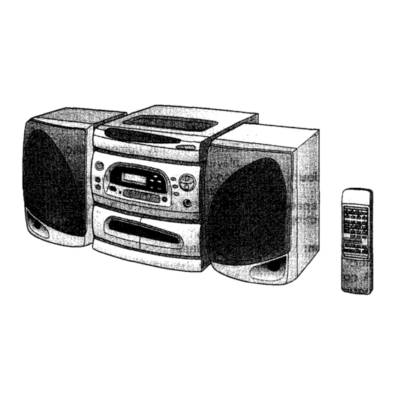
Illustration: CD-C250NCP-C2
Illustration: CD-C260X/CP-C250
DIGITAL AUDIO
SPECIFICATIONS.. ............................................................................................................................................................
VOLTAGE SELECTION ................................................. ....................................................................................................
AC POWER SUPPLY CORD AND PLUG ..........................................................................................................................
NAMES OF PARTS .......................................................................................... __. ............................................................... 3
OPERATION MANUAL ......................................................................................................................................................
DISASSEMBLY ......................................... .........................................................................................................................
REMOVING AND REINSTALLING THE MAIN PARTS .....................................................................................................
ADJUSTMENT .................................................................................................................................................................
TROUBLESHOOTING (CD SECTION) ............................................................................................................................
FUNCTION TABLE OF IC ................................................................................................................................................
LCD SEGMENT.. ..............................................................................................................................................................
NOTES ON SCHEMATIC DIAGRAM ...............................................................................................................................
TYPES OF TRANSISTOR ................................................................................................................................................
BLOCK DIAGRAM.. ...........................................................................................................................................................
WAVEFORMS OF CD CIRCUIT ......................................................................................................................................
SCHEMATIC DIAGRAM /WIRING SIDE OF P.W.BOARD .............................................................................................
REPLACEMENT PARTS LIST / EXPLODED VIEW
Difference between CD-C250X and CD-C260X
l
Front Panel.and CD Cover but their functions are the same.
In the interests of user-safety the set should be restored to its original
l
condition and only parts identical to those specified be used.
No. S8531 CDC250XK
Page -' -
2
2
2
5
6
8
10
12
21
22
22
23
27
29
Advertisement
Table of Contents

Related Manuals for Sharp CD-C250X BK


Summary of Contents for Sharp CD-C250X BK
-
Page 1: Table Of Contents
No. S8531 CDC250XK Illustration: CD-C250NCP-C2 Difference between CD-C250X and CD-C260X Front Panel.and CD Cover but their functions are the same. In the interests of user-safety the set should be restored to its original condition and only parts identical to those specified be used. Illustration: CD-C260X/CP-C250 DIGITAL AUDIO Page -‘... -
Page 2: Specifications
FOR A COMPLETE DESCRIPTION OF THE OPERATION OF THIS UNIT, PLEASE REFER TO THE OPERATION MANUAL. General Type: source: A C 11 O/l 2712201230-240 V, 50160 Hz player Power consumption: 80 W Signal readout: Non-contact, 3-beam semi- Dimensions: Width; 270 mm (1 O-5/8”) conductor laser pickup Height;... -
Page 3: Names Of Parts
Illustration: CD-C250X panel Disc Tray Disc Number Indicator CD Play Indicator: ) Record Indicator Preset Channel Indicator FM Stereo Indicator: co 14. Function/Track Number/CD Counter/ Memory Indicator Power Switch Record Start Button: 0 Stand-By Indicator 6171819 2223 Remote Control Sensor Volume Up/Down Buttons: A/V Tuning Up/Down Buttons: A/V Reset Button... - Page 4 Rear panel AM Loop Aerial Socket Voltage Selector Speaker section Left speaker Right speaker Woofer TO. Speaker Wire Remote control Remote Control Transmitter Window Track Up/Cue Button: + IH Random Button Memory Button Pause Button: (TAPE 2) Stop Button: n (TAPE 2) Rewind Button: t( (TAPE 2) Play Button: ) (TAPE 2) Fast Forward Button: H...
-
Page 5: Operation Manual
n Proper use of the remote control Aim the remote control at the remote control sensor within Notes concerning use: operation becomes erratic. control and the sensor on the main unit with a soft cloth. interfere with operation. Change the lighting or the direc- tion of the unit. -
Page 6: Disassembly
Illustration: CD-C250X Caution on Disassembly Follow the below-mentioned notes when disassembling the unit and reassembling it, to keep it safe and ensure excellent performance: 1. Take cassette tape and compact disc out of the unit. 2. Be sure to remove the power supply plug from the wall outlet before starting to disassemble the unit. - Page 7 Switch PWB Turntable Tape Mechanism Figure 7-1 CD Player Unit Figure 7-4 xl Omm 02.6 hanger anism Figure 7-2 xl Omm Care when installing the CD changer mechanism. Install the CD changer mechanism on the CD player base after the shift lever has been set in the highest position. CD Servo PWB Figure 7-5 Figure 7-6...
-
Page 8: Removing And Reinstalling The Main Parts
Record/Playback Perform steps 1, 2, 3, 4, 6 and 8 of the disassembly method to remove the tape mechanism. How to remove the record/playback and erase heads (TAPE 2) (See Fig. 8-l.) in the direction of the arrow @, and remove the record/ playback head upwards. - Page 9 Perform steps 1, 2, 3, 10, 11, 12, and 13 of the disassembly method to remove the CD mechanism. How to remove the loading motor (See Fig. 9-1) 2. Remove the screws (A2) x 2 PCS., to remove the loading motor.
-
Page 10: Adjustment
Driving Force Check Specified Value Torque Meter AM IF/RF Play: TW-2412 Tape 1: Over 80 9 Signal generator: 400 Hz, 30%, AM modulated Tape 2: Over 80 g Frequency Test Stage / Frequency Display Adjusting Connection Parts Specified Value Torque Meter 450 kHz 1,602 kHz or T351 Tape 1... - Page 11 Setting the test mode Any one of 4 test modes can be set by pressing several keys as follows TEST : CD operation test TEST 4 mode Function - CD test mode Setting of TEST 4 mode IL is not performed. <STOP>...
-
Page 12: Troubleshooting (Cd Section)
When the CD does not function When the CD section does not operate When the objective lens of the optical pickup is dirty,this section may not operate.Clean the objective lens,and check the playback operation.When this section does not operate even after the above step is takencheck the following items. - Page 13 Check the SW1 and the wiring from the IC701 pin 8 to the SWl. Is there following voltage input in specific state of IC701 pin 8’ 7 Close state: OV Intermediate state between open state and close state: 5V Is H output to IC701 pin 70 or 71 for 5 seconds when the OPEN/ Check the wiring of the lC701 pins 70 and 71, IC901 pins 1 CLOSE key is pressed?105 is defective.
- Page 14 6 BYTE 6 BYTE COMM BYTE DATA 100 ms interval Figure 14-1 CD microcomputer -- Main microcomputer data transmission CK: 262 kHz or less 8 BIT COMM DATA DATA and COMM are read at rise of SCK. LSB FIRST Figure 14-2 CD microcomputer -- Main microcomputer data transmission CNP 7 5 Pin 20ms...
- Page 15 Check the Focus - HF svstem. Focus search OK Does the output waveform of ICi(lG)(FD) match that shown in Check the area around IC5CNP2. Fig. 15-i? Focus search is performed Check the IC1(50)(CLK) line, 4MHz. two times Check the microcomputer data on pins (51)(CL), (52)(DAT) and when play operation is disc.
- Page 16 Check waveform of ICl pin 7 (TE). Check the periphery of IC 1 appears, and no-disc state apperas soon. Although IL is possible, play is impossible. Check the periphery of program top cannot be reached. Check the VCO-PLL system. Data cannot be read. 1.00 v ICI @TE 5 ms...
- Page 17 Play operation is performed when disc exits. Although HF waveform is normal, Check PDO waveform (Fig. 17-1). Error Check the ICl pins 43 and 44, IC2 pins 3,5,7, 10, and 11. Stop --> Play As VCO freque- ncy is locked at 4.32 M Hz, voltage of PDO rises and stabili-...
-
Page 18: Function Table Of Ic
Pin No. Port Name Terminal Name input/Output Function SQOUT Input Servo/signal control data input COIN output Servo AMP, servo/signal control command output CQCK output Servo AMP, servo/signal control clock output output Servo AMP, servo/signal control R/W control Connect to AD converter reference voltage input terminal GND. Connect to AD converter reference voltage input terminal GND. - Page 19 Figure 19 BLOCK DIAGRAM OF IC...
- Page 20 T e r m i n a l N a m e hpUt/OUtput F u n c t i o n Pin No. Port Name Input Supply voltage of 0-VL2 to LCD In/Output CMOS input level CMOS 3 state output. (8 bit I/O port.) In/Output CMOS input level CMOS 3 state output.
-
Page 21: Lcd Segment
COMO COM2 COM3... -
Page 22: Notes On Schematic Diagram
. Resistor: . The indicated voltage in each section is the one measured by To differentiate the Units of resistors, the symbol as K and M Digital Multimeter between such a section and the chassis are used: the symbol K means 1000 ohm and the symbol M with no signal given. - Page 23 PICKUP UNIT FOCUS COtL TRACKING COIL C O N T R SPIN SLIDE MOTOR MOTOR LASER RESET RESET PICKUP IN PU-IN SW Figure 23 BLOCK DIA - 2 3 -...
-
Page 24: Block Diagram
XOUT DATA TO MAIN MICON CNP7 LASER RESET REGULATOR - 2 4 -... - Page 25 S O 3 0 1 FM ANTENN* TP?“, P L L C O N T R O L L E R Figure 25 BLOCK C...
- Page 26 S Y S T E M C O N T R O L A M P VOLTAGE REGULATOR VOLTAGE REGULATOR VOLTAGE REGULATOR LOCK DIAGRAM (2/2)
-
Page 27: Waveforms Of Cd Circuit
STOP-PLAY FOCUS- SERCH 5.0 v 0.50 v 50ms 5.0 v 0.50 v 5.0 v REVIEW REVIEW 5.0 v 0.50 v 5.0 v... - Page 28 PLAY 10.0 v TCD-712 0.50 v PLAY NORMAL DISC 20ms PLAY TCD-712 (140mm) 50ms 1.00 v 50ms 2.00 v...
-
Page 29: Schematic Diagram /Wiring Side Of P.w.board
CNSM I TAPE MOTOR RECORD/PLAYBACK HEAD ERASE HEAD The numbers @ to @ are waveform numbers shown in page 27,28. Figure 29 WIRING SIDE ( - 2 9 -... - Page 30 ( C D S E R V O PWB-BI PLAYBACK HEAD m-i- D MOTOR SIDE OF P.W.BOARD (i/2)
- Page 31 The numbers 0 to @ are waveform numbers shown in page 27, 28. NOTES ON SCHEMATIC DIAGRAM can be found on page 22. Figure 31 SCHEMATIC DL...
- Page 32 I I -...
- Page 33 L-CH SPEAKER TERMINAL Figure 33 WIRING SIDE t - 3 3 -...
- Page 34 CNS4 AC POWER SUPPLY CORD A C 110/127/220/...
- Page 35 I ? - NOTES ON SCHEMATIC DIAGRAM can be found on page 22. Figure 35 SCHEMATIC DI, - 3 5 -...
- Page 36 S I G N A L P O W E R PWB-A2 - - - - - - - - ___-___-_ - - - - - - -...
- Page 37 T A P E D E C K PWB-C . NOTES ON SCHEMATIC DIAGRAM can be found on page 22. Figure 37 SCHEMATI - 3 7 -...
- Page 38 - 3 8 -...
- Page 39 SYSTEM CONTROL MICROCOMPUTER NOTES ON SCHEMATIC DIAGRAM can be found on page 22. Figure 39 SCHEMATIC 0 --- ~~ .-...
- Page 41 . 5v COVI 4 . 9v . 4v iov/ 4 . 9v i v iovj 4 . 8V (FM FRONT E N D , 4 . 9v 1 2 3 7 5 ohrr 0. 0 33 OTHER : FM . NOTES ON SCHEMATIC DIAGRAM can be found on page 22. Figure 41 SCHEMATll...
- Page 42 SWITCHING l FI...
- Page 43 “HOW TO ORDER REPLACEMENT PARTS” To have your order filled promptly and correctly, please furnish the following information. 1 . M O D E L N U M B E R 2 . R E F . N O . 3.
- Page 44 PART NO. CODE DESCRIPTION PART NO. DESCRIPTION 47 ,uF,lOV,ElectroIytic VHCKV13 1 OA2-F 0.001 pF,5OV VHEMTZJ 5R6B- 1 ZD351 ZD922 ZD923 FILTERS TRANSFORMERS T302 T304 COILS L302 A Da L353 1901,902 VARIABLE RESISTOR VR351 [FM Mute Level] VIBRATORS x351 Electrolytic X352 XL701 CAPACITORS There are two types of capacitors available and they can be identified from eacl...
- Page 45 PART NO. DESCRIPTION CODE PART NO. DESCRIPTION CODE 0.22 pF,50V,Electrolytic Polypropylene Cl56 22 /1F,16V,Electroiytic c443 c444 c735 C316 C736 c737 c739 c331 C756 C332 c334 c335 C336 (Serial No.50600001 -507 X X X X X Only) C352 c355 C356 c357 ca21 c359 C822...
- Page 46 PART NO. DESCRIPTION CODE PART NO. DESCRIPTION CODE R143 R147 R148 R153 R154 R159 R178 R179 R301 R302 R303 R309 R312 R316 R317 R319 R320 R323 R324 R330 R331 R351 R352 R353 R354 R356 R358 R360 R116 R367 R368 R376 R127 R377 R379...
- Page 47 DESCRIPTION PART NO. CODE PART NO. DESCRIPTION CODE R386 R757 R393 R395 R769 R779 R781 R423 R424 R460 R475 6 kohms,l/6W ’ R902 R702 R904 R703 R905 R704 R706 R707 R709 R710 R917 R922 R923 R924 R927 R720 R929 R930 R727 R931 R932...
- Page 48 PART CODE PART DESCRIPTION CODE DESCRIPTION [X-Bass] SW706 [Equalizer] (Serial No.50600001 SW708 - 5 0 7 X X X X X O n l y ) [Volume Down] CNP951 [CD-Rewind/Tape 2 -Preset Down] SW710 [Tuning Down] SW712 SW715 SW716 (Serial No.50600001 - 5 0 7 X X X X X Only) SW718 [Disc Number-l]...
- Page 49 PART NO. DESCRIPTION CODE PART NO. DESCRIPTION CODE [Tape 1306 [Tape 21 Pickup Unit Item) [Tape [Tape [Tape [Slide] [Tape [Pickup in] CABINET PARTS MSPRPO 0 OSAWFW Front Panel [Tape II (Not Replacement Item) [Tape L e v e r L e v e r [Tape Tape 1...
- Page 50 PART DESCRIPTION CODE PART DESCRIPTION CODE Gi TAR0041AWSA J B a c k B o a r d (Serial No.506X X X X X -507X X X X X Only) ACCESSORIES/PACKING PARTS L e f t / R i g h t [260X] _ Left/Right [250X] Front Accessories...
- Page 51 PART DESCRIPTION CODE SPEAKER BOX PARTS PACKING PARTS Speaker...
- Page 52 Figure 10 CD MECHANISM EXPLODED VIEW...
- Page 53 - 2 0 BELT CONNECTION Motor Figure 11 TAPE MECHANISM EXPLODED VIEW...
- Page 54 603x2 ' 2 3 4 Figure 12 &INET EXPLODES VIEW (l/2)
- Page 55 , 2 1 4 - l -‘ \, ‘ 627 Figure 13 CABINET EXPLODED VIEW (2/2)
- Page 56 TWEETER BLACK LINE WOOFER Cl ,2 TWEETER WOOFER Figure 14 SPEAKER BOX EXPLODED VIEW Printed in Japan Writer and Editor: Quality & Reliability Control Center of Communication & Audio Systems Group, Sharp Corp.
Need help?
Do you have a question about the CD-C250X BK and is the answer not in the manual?
Questions and answers