Yamaha R-N500 Service Manual
Hide thumbs
Also See for R-N500:
- Owner's manual (420 pages) ,
- Owner's manual (20 pages) ,
- Firmware update (4 pages)
Table of Contents
Advertisement
This manual has been provided for the use of authorized Yamaha Retailers and their service personnel.
It has been assumed that basic service procedures inherent to the industry, and more specifi cally Yamaha Products, are already known
and understood by the users, and have therefore not been restated.
WARNING:
IMPORTANT:
The data provided is believed to be accurate and applicable to the unit(s) indicated on the cover. The research, engineering, and service
departments of Yamaha are continually striving to improve Yamaha products. Modifi cations are, therefore, inevitable and specifi cations
are subject to change without notice or obligation to retrofi t. Should any discrepancy appear to exist, please contact the distributor's
Service Division.
WARNING:
IMPORTANT:
■ CONTENTS
TO SERVICE PERSONNEL ............................................2
FRONT PANEL ...............................................................3
REAR PANELS ...........................................................3-5
REMOTE CONTROL PANEL ..........................................6
SPECIFICATIONS .......................................................6-8
INTERNAL VIEW ............................................................9
SERVICE PRECAUTIONS ..............................................9
DISASSEMBLY PROCEDURES ............................. 10-12
UPDATING FIRMWARE .......................................... 13-15
SELF-DIAGNOSTIC FUNCTION ............................ 16-35
POWER AMPLIFIER ADJUSTMENT ............................36
NETWORK RECEIVER
R-N500
SERVICE MANUAL
IMPORTANT NOTICE
Failure to follow appropriate service and safety procedures when servicing this product may result in personal injury,
destruction of expensive components, and failure of the product to perform as specifi ed. For these reasons, we advise
all Yamaha product owners that any service required should be performed by an authorized Yamaha Retailer or the
appointed service representative.
The presentation or sale of this manual to any individual or fi rm does not constitute authorization, certifi cation or
recognition of any applicable technical capabilities, or establish a principle-agent relationship of any form.
Static discharges can destroy expensive components. Discharge any static electricity your body may have
accumulated by grounding yourself to the ground buss in the unit (heavy gauge black wires connect to this buss).
Turn the unit OFF during disassembly and part replacement. Recheck all work before you apply power to the unit.
DISPLAY DATA .......................................................37-38
IC DATA ...................................................................39-49
BLOCK DIAGRAMS ................................................50-51
WIRING DIAGRAMS ...............................................52-53
PRINTED CIRCUIT BOARDS .................................54-69
PIN CONNECTION DIAGRAMS ...................................70
SCHEMATIC DIAGRAMS .......................................71-78
REPLACEMENT PARTS LIST ................................79-89
REMOTE CONTROL ...............................................90-92
SETUP MENU .........................................................93-98
Advertisement
Table of Contents

Related Manuals for Yamaha R-N500


Summary of Contents for Yamaha R-N500
-
Page 1: Table Of Contents
This manual has been provided for the use of authorized Yamaha Retailers and their service personnel. It has been assumed that basic service procedures inherent to the industry, and more specifi cally Yamaha Products, are already known and understood by the users, and have therefore not been restated. -
Page 2: To Service Personnel
R-N500 ■ TO SERVICE PERSONNEL AC LEAKAGE 1. Critical Components Information WALL EQUIPMENT TESTER OR OUTLET UNDER TEST EQUIVALENT Components having special characteristics are marked ⚠ and must be replaced with parts having specifications equal to those originally installed. 2. Leakage Current Measurement (For 120V Models Only) -
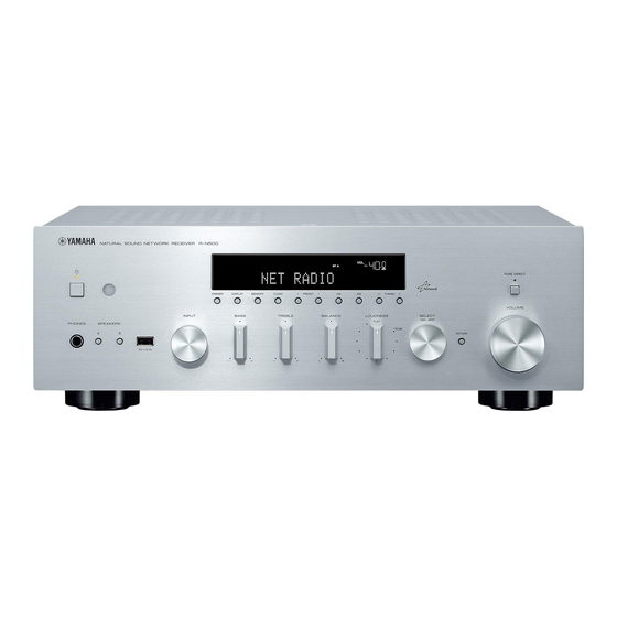
Page 3: Front Panel
R-N500 ■ FRONT PANEL ■ REAR PANELS U, C models R, S models... - Page 4 R-N500 K model A model B, G models...
- Page 5 R-N500 L model...
-
Page 6: Remote Control Panel
R-N500 ■ REMOTE CONTROL PANEL ■ SPECIFICATIONS ■ Audio Section RAS9 Minimum RMS Output Power (Power Amp. Section) (20 Hz to 20 kHz, 0.04 % THD, 8 ohms / L/R drive) ..................80 W + 80 W Dynamic Power Per Channel (IHF) 8 / 6 / 4 / 2 ohms .......... - Page 7 R-N500 Gain Tracking Error (+16.5 to -80 dB) Finish ..................0.5 dB or less U, C, R, A, B, G, L, S models .......... Black color U, C, R, K, A, B, G, L, S models ........Silver color Optical Jack, Coaxial Jack Support Frequencies ................
- Page 8 R-N500 • DIMENSIONS ø 60 Top view 335 (13-1/4") (2") Front view 435 (17-1/8") Unit: mm (inch)
-
Page 9: Internal View
R-N500 ■ INTERNAL VIEW Top view OPERATION (2) P.C.B. MAIN (3) P.C.B. MAIN (4) P.C.B. (R, S models) MAIN (9) P.C.B. DIGITAL P.C.B. MAIN (2) P.C.B. AM/FM TUNER OPERATION (3) P.C.B. OPERATION (5) P.C.B. OPERATION (4) P.C.B. MAIN (10) P.C.B. -
Page 10: Disassembly Procedures
R-N500 ■ DISASSEMBLY PROCEDURES (Remove parts in the order as numbered.) Disconnect the power cable from the AC outlet. 1. Removal of Top Cover a. Remove 4 screws ( ① ), 4 screws ( ② ) and screw ( ③ ). (Fig. 1) b. - Page 11 R-N500 3. Removal of Sub-chassis Unit 5. Removal of Amp Unit and Power Transformer a. Remove 2 screws ( ⑥ ). (Fig. 2) a. Remove 2 screws ( ⑩ ) and screw ( ⑪ ). (Fig. 2) b. Remove CB21, CB61, CB426, CB461, CB463 and b.
- Page 12 R-N500 When checking the MAIN (1) P.C.B.: • Spread the rubber sheet and the cloth. Then place this unit on the cloth upside down. (Fig. 5) • Remove 6 screws ( ⑭ ) and then remove the bottom cover. (Fig. 5) ⑭...
-
Page 13: Updating Firmware
R-N500 ■ UPDATING FIRMWARE When the following parts are replaced, the firmware must be updated to the latest version. DIGITAL P.C.B. ● Confirmation of firmware version Before and after updating the firmware, check the firmware version by using the self-diagnostic function menu. - Page 14 R-N500 ● Operation Procedures Disconnect the power cable of this unit from the AC outlet. 1. Press the “ ” (Power) key to the ON position. (Fig. 1) 2. Insert the USB storage device to the USB jack. (Fig. 1) 3.
- Page 15 R-N500 List of Error Messages Display E R R O R ! x x x x Error number Error Number Error Message Cause 0001 Microprocessor clearing error Microprocessor failure 0002 Microprocessor writing error 0004 Microprocessor checksum error Microprocessor failure / Mismatch of checksum...
-
Page 16: Self-Diagnostic Function
R-N500 ■ SELF-DIAGNOSTIC FUNCTION This unit has self-diagnostic functions that are intended for inspection, measurement and location of faulty point. There are 14 main menu items, each of which has sub-menu items. Listed in the table below are main menu items and sub-menu items. - Page 17 R-N500 Main menu Sub-menu PROTECTION HISTORY 1. HISTORY 1 1. POWER PORT 1. LAST INPUT 1. LAST VOLUME LEVEL 2. HISTORY 2 2. POWER PORT 2. LAST INPUT 2. LAST VOLUME LEVEL 3. HISTORY 3 10 3. POWER PORT 11 3. LAST INPUT 12 3.
- Page 18 R-N500 ● Starting Self-Diagnostic Function While pressing the “PRESET ” and “DIMMER” keys, press the “ ” (Power) key to turn on the power, and release those 2 keys. The self-diagnostic function mode is activated. Keys of this unit (Power) While pressing these keys, turn on the power.
- Page 19 R-N500 ● Display provided when Self-Diagnostic Function started The display is as described below depending on the situation when the power to this unit is turned off. 1. When the power is turned off by usual operation: “NO PROTECT” is displayed. Then “A1-1. NORMAL” is displayed in a few seconds.
- Page 20 R-N500 2-2. When the protection function worked due to abnormal DC output. H: Displayed when the voltage is HIGHER than upper limit D C P R T : x x x H L: Displayed when the voltage is LOWER than lower limit xxx: A/D conversion value of voltage at the moment when the protection function worked (Reference voltage: 3.3 V=255)
- Page 21 R-N500 2-4. When the protection function worked due to excessive heatsink temperature. H: Displayed when the voltage is HIGHER than upper limit T M P x P R T : x x x L L: Displayed when the voltage is LOWER than lower limit xxx: A/D conversion value of voltage at the moment when the protection function worked (Reference voltage: 3.3 V=255)
- Page 22 R-N500 ● Operation procedure of Main menu and Sub-menu There are 14 main menu items, each of which has sub-menu items. Main menu selection Select the main menu using “AM” (forward) and “FM” (reverse) keys. Sub-menu selection Select the sub-menu using “TUNING ” (forward) and “TUNING ” (reverse) keys.
- Page 23 R-N500 ● Details of Self-Diagnostic Function menu A1. AUDIO SET This menu is used to check audio signal route. A1-1. NORMAL The audio signal input to LINE 1 jack is output. A 1 - 1 N O R M A L A1-2.
- Page 24 R-N500 D1. FL CHECK This menu is used to check operation of the FL display. FL display D1-1. INITIAL DISPLAY D1-2. ALL SEGMENT OFF D1-3. ALL SEGMENT ON * After check, change to next menu at once. D1-4. CHECK PATTERN 1 Example Lighting on segments in lattice.
- Page 25 R-N500 U1. USB This menu is used to check the audio signal route from USB storage device. U1-1. USB FRONT 1 TRACK The 1st music file stored in the USB storage device connected to the USB jack is reproduced. * Copy 2 or more music files from PC to the root folder of the USB storage device in advance.
- Page 26 R-N500 N1-3. LINE NOISE 100 MDI Not for service. N 1 - 3 L N M D I 1 0 0 N1-4. LINE NOISE 100 MDIX Not for service. N 1 - 4 L N M D I X 1 0 0 N1-5.
- Page 27 R-N500 C1. ACCESS CHECK This menu is used to check the communication and bus line connection between devices on DIGITAL P.C.B. C1-1. ALL The total detection result of sub-menus from C1-2 to C1-4 is displayed. C 1 - 1 A L L : O K...
- Page 28 R-N500 C2. NETWORK IC CHECK This menu is used to check the communication and bus line connection between devices related to network. C2-1. ALL The total detection result of sub-menus from C2-2 to C2-4 is displayed. C 2 - 1...
- Page 29 R-N500 P1. AD DATA CHECK This menu is used to display the A/D conversion value of the microprocessor which detects panel keys and protection functions by using the sub-menu. When “P1-7. KEY” sub-menu is selected, keys become inoperable due to detection of the values of all keys. However, it is possible to advance to the next menu by turning the VOLUME knob.
- Page 30 R-N500 P1-3. TMP Temperature of the heatsink (THM) is detected. The voltage at 122 pin (THM1)/123 pin (THM2) /110 pin (THM3) of IC21 is displayed. Normal value THM1: 54 to 255 (U, C, R, K, A, B, G, S models)
- Page 31 R-N500 P1-7. KEY Panel key is detected. When the A/D conversion value of the panel key becomes out of the specified range, normal operation will not be available. In that case, check the constant of voltage dividing resistor, solder condition, etc. Refer to table.
- Page 32 R-N500 P2. PROTECTION HISTORY This menu is used to display the history of protection function. In the history 1 to 4, the setting information for operation of each protection function will be stored. All history of protection function and setting information will be erased by pressing the “RETURN” key.
- Page 33 R-N500 T1. TROUBLE SHOOTING INFORMATION This menu is used to display the operating time and operation frequency of this unit. The operating time and operation frequency during the self-diagnostic function mode will not be stored. T1-1. OPERATING TIME The operating time of this unit is displayed.
- Page 34 R-N500 S1. FACTORY PRESET This menu is used to reserve/inhibit initialization of the back-up IC (EEPROM: IC22 on DIGITAL P.C.B.). S1-1. PRESET INHIBIT (Initialization inhibited) S 1 - 1 P R E S E T I N H I Initialization of the back-up IC is not executed.
- Page 35 Destination U / C / R (R, S) / K / A / G (B, G, F) / L Not for service. Model name N5 (R-N500) S4-2. VERIFY Not for service. S 4 - 2 V e r i f y 2 5 5 0 0...
-
Page 36: Power Amplifier Adjustment
R-N500 ■ POWER AMPLIFIER ADJUSTMENT 1. Right after power is turned on, confirm that the voltage 1. 電源投入直後、R2050 (Rch) 、R2049 (Lch)の端子間 across the terminals of R2050 (Rch) and R2049 (Lch) 電圧を測定し、0.05 mV から 2.5 mV の間であることを are within the confines of 0.05 mV to 2.5 mV. -
Page 37: Display Data
R-N500 ■ DISPLAY DATA ● V4001 : 18-MT-11GNAK (OPERATION (1) P.C.B.) PATTERN AREA ● PIN CONNECTION Pin No. 68 67 Connection F2 NX 29 28 Pin No. Connection Note : 1) F1, F2 ..Filament pin 2) NP ..No pin 3) NX .. - Page 38 R-N500 ● ANODE CONNECTION 1G-14G –...
-
Page 39: Ic Data
R-N500 ■ IC DATA IC951: DM860A (DIGITAL P.C.B.) Network microprocessor * No replacement part available. General Purpose Security Engine Timing Engine on-chip RAM RESET, BOOT_SEL CLOCKS Reset, Boot, OTP 2 PLLs, 3 DCOs 64 kBytes master AV0 Port slave 4xAudio, 1xVideo... - Page 40 R-N500 AV-Port 0 Pin No. Function Name Detail of Function Audio/video data. AV0DATA[3:0] Several formats are supported. Video data, together with AV0DATA[3:0]: AV0DATA[3:0] = video[3:0] AV1DATA[3:0] AV1DATA[3:0] = video[7:4] Data clock. Depending on the AV-Port 0 configuration, this clock is a bit- or byte-clock which is used to AV0CLK transmit or receive the AV0DATA[*] synchronously.
- Page 41 R-N500 Serial Peripheral Interface (SPI) Pin No. Function Name Detail of Function SPIDIN SPI data receive. SPIDOUT SPI data transmit. SPICLK SPI clock. Multi-master mode: Chip-select input (used to detect bus conflict). SPINCS0 Master only mode: Chip-select 1 output. Slave mode: Chip-select input.
- Page 42 R-N500 Pin No. Function Name Detail of Function Chip select signals. The active memory range for NCS[n] (active low) can be configured. • NCS[0] supports SRAM, can be used for booting. NCS[3:0] • NCS[1] supports SDRAM or SRAM. • NCS[2] supports SRAM.
- Page 43 R-N500 USB 2.0 OTG Pin No. Function Name Detail of Function USBD+ Positive data line that is connected to the serial USB cable. USBD– Negative data line that is connected to the serial USB cable. USBID USB ID pin of mini-AB receptacle.
- Page 44 R-N500 SSM Interface Pin No. Function Name Detail of Function SSMD[7:0] Data lines. SSMCLK Clock output. SSMCMD Command output. SSMCP Card power input (high = off). SSMWP Write protect input (low = protect). External PLL Pins Pin No. Function Name Detail of Function External oscillator inputs, typically coming from an external VCO.
- Page 45 R-N500 Power Supply Pins Pin No. Function Name Detail of Function Pin No. Function Name Detail of Function VDD33 I/O power supply (+3.3 V). Ground (0 V). VDD33USB Power supply (+3.3 V) for USB interface. Ground (0 V). VSS33USB VDD33PLL Power supply (+3.3V) for PLL.
- Page 46 R-N500 IC21: R5F3651TNFC (DIGITAL P.C.B.) Microprocessor * No replacement part available. Port P0 Port P1 Port P2 Port P3 Port P4 Port P5 Port P12 Port P13 VCC2 ports Internal peripheral functions System clock generator UART or clock synchronous serial I/O...
- Page 47 R-N500 Function Name Port Name Detail of Function (P.C.B.) VREF VREF AD standard voltage AVCC AVCC Microprocessor power supply SIN4 EEP_MISO EEPROM / Expansion Flash synchronization data input SOUT4 EX_MOSI FL driver / EEPROM / Expansion Flash synchronization data output...
- Page 48 R-N500 Function Name Port Name Detail of Function (P.C.B.) P13_3 HPRY Headphone relay control P13_2 SPRY_B (SPRY_SB_BA) Speaker relay control (SP B) P13_1 (no_use) P13_0 SPRY_5CH Speaker relay control (Front/Center/Sorround) P5_3 MT_N_Z2 (MT_N_SB) Mute control (Zone2) P5_2 SEL_NDAC L: Bco output / H: No input...
- Page 49 R-N500 Function Name Port Name Detail of Function (P.C.B.) 104 P0_7 DAC_N_CS DAC chip select 105 P0_6 NCPU_AMUTE NET audio mute demand 106 AN0_5 PS3_PRT PS protection detection 3 107 AN0_4 PS2_PRT PS protection detection 2 108 AN0_3 (reserve) AD spare...
-
Page 50: Block Diagrams
R-N500 ■ BLOCK DIAGRAMS • See page 78 → • See page 75–77 → MAIN OPERATION SCHEMATIC DIAGRAM SCHEMATIC DIAGRAM PURE DIRECT IC431 SPEAKER A RECL2 / RECR2 Selector and E-Vol. Power Amplifier BD3473KS2 LINE3 IC461 INL1 / INR1 NJM2068MD... - Page 51 R-N500 Power Supply Section Block Diagram Speaker Impedance relay IC25 +5.5V +3.3M Microprocessor (IC21)/Standby LED/Remote/key input Power +3.3M Power Amplifier Transformer RY204 IC24 D2019 C2044 +3.3S Control circuits around Microprocessor +3.3S +3.3S_PO IC67 C2045 +3.3D RY204 Power Amplifier DCDC_PO Q401 +3.3DSP DSP (IC41), SDRAM (IC42), FLASH ROM (IC43)
-
Page 52: Wiring Diagrams
R-N500 ■ WIRING DIAGRAMS Fix the wires by PN279 • OVERALL ASSEMBLY so as not to touch with HS202 Fix the wire by PN202 wires (Power transformer–CB206 so as not to touch with HS202 Flexible flat cable Power transformer–CB207 wire (Power transformer–CB207) - Page 53 R-N500 • AMP UNIT to DIGITAL (CB23) to DIGITAL (CB25) 40 mm (1-5/8") PN261 15 mm PN262 PN261 (5/8") CB264 MAIN (2) MAIN (2) CB263 CB264 W2601 PN263 MAIN (6) CB263 W2601 PN262 PN263 CB266 Side view Top view Flexible flat cable...
-
Page 54: Printed Circuit Boards
R-N500 ■ PRINTED CIRCUIT BOARDS • Semiconductor Location Ref no. Location Ref no. Location Ref no. Location Ref no. Location Ref no. Location D205 IC61 IC69 Q201 Q601 IC21 IC63 IC70 Q207 Q602 IC22 IC64 IC951 Q208 Q604 IC65 IC952... - Page 55 R-N500 DIGITAL (Side B) IC954 • Semiconductor Location Ref no. Location IC71 IC954 Q202 Q203 Q204 Q205 Q206...
- Page 56 R-N500 OPERATION (1) (Side A) DIGITAL (CB21) MAIN (5) (CB274) MAIN (1) (CB205) W4003 CB403 CB402 +3.3DSP POWER PD_LED indicator DGND MAIN (8) (CB276) Remote control sensor TUNING PRESET CLEAR MEMORY DISPLAY DIMMER DGND VOL_RB VOL_RA +3.3DSP DGND MAIN (7)
- Page 57 R-N500 OPERATION (1) (Side B) IC401 IC402 OPERATION (9) (Side B) • Semiconductor Location Ref no. Location Ref no. Location D4013 D4001 D4002 IC401 D4003 IC402 D4004 Q4001 D4005 Q4002 D4006 Q4003 D4007 Q4004 D4008 Q4005 D4010 Q4006 Q4007 D4011...
- Page 58 R-N500 Safety measures • Some internal parts in this product contain high voltages and are dangerous. Be sure to take safety measures during servicing, such as wearing insulating gloves. • Note that the capacitors indicated below are dangerous even after the power is turned off because an electric charge remains and a high voltage continues to exist there.
- Page 59 R-N500 OPERATION (2) OPERATION (3) (Side B) (Side B) IC431 • Semiconductor Location Ref no. Location K, A, B, G, L models D4301 D4302 D4303 D4304 D5402 D5403 D5405 D5406 D5407 D5408 D5409 IC431 IC432...
- Page 60 R-N500 OPERATION (4) OPERATION (5) (Side A) (Side A) OPTICAL COAXIAL PS2_PRT +5DSP PS2_PRT AV1_D CD_L CD_L AV2_D CD_E CD_E DGND CD_R CD_R AV3_D AV4_D DGND +12A +12A NETL NETE NETL NETE NETE NETR NETE NETR NETE NETL NETR OPERATION (3)
- Page 61 R-N500 OPERATION (4) OPERATION (5) (Side B) (Side B) IC436 OPERATION (6) (Side B) K, B, G, L models • Semiconductor Location Ref no. Location D4351 D4401 IC436 IC461 Q4601 Q4602 IC461...
- Page 62 R-N500 OPERATION (7) OPERATION (8) (Side A) (Side A) BASS TREBLE BALANCE LOUDNESS – – FLAT -30 dB AGND AGND AGND OPERATION (10) OPERATION (11) (Side A) (Side A) OPERATION (6) (CB462) PHONES DIGITAL JK426 (CB952) W4272 CB427 (USB jack)
- Page 63 R-N500 OPERATION (7) OPERATION (8) (Side B) (Side B) IC466 OPERATION (10) OPERATION (11) (Side B) (Side B) • Semiconductor Location Ref no. Location D4261 D4262 IC466...
- Page 64 R-N500 Safety measures • Some internal parts in this product contain high voltages and are dangerous. Be sure to take safety measures during servicing, such as wearing insulating gloves. • Note that the capacitors indicated below are dangerous even after the power is turned off because an electric charge remains and a high voltage continues to exist there.
- Page 65 R-N500 MAIN (1) (Side B) IC201 • Semiconductor Location Ref no. Location D2001 D2002 D2003 D2004 K, B, G, L models D2005 D2006 D2007 D2008 D2009 D2012 D2013 D2017 D2018 D2021 D2023 D2024 D2027 IC201 Q2001 Q2002 Q2005 Q2006 Q2007...
- Page 66 R-N500 MAIN (2) (Side A) MAIN (1) MAIN (1) (CB203) (CB204) MAIN (6) (CB266) CB262 CB261 W2601 CB263 CB264 DIGITAL (CB25) DIGITAL (CB23) MAIN (3) MAIN (4) MAIN (5) (Side A) (Side A) (Side A) R, S models DIGITAL (CB24)
- Page 67 R-N500 MAIN (2) (Side B) • Semiconductor Location Ref no. Location D2781 D2782 D2783 D2784 D2785 Q2781 Q2782 Q2783 MAIN (3) MAIN (4) MAIN (5) (Side B) (Side B) (Side B) R, S models...
- Page 68 R-N500 MAIN (6) MAIN (7) MAIN (8) (Side A) (Side A) (Side A) OPERATION (1) (CB407) IC267 DGND VOL_RB CB276 VOL_RA +3.3DSP CB266 OPERATION (1) (CB404) PURE DIRECT indicator VOLUME MAIN (2) (W2601) • Semiconductor Location Ref no. Location D2751...
- Page 69 R-N500 MAIN (6) MAIN (7) MAIN (8) (Side B) (Side B) (Side B) • Semiconductor Location Ref no. Location Q2751 MAIN (9) MAIN (10) (Side B) (Side B)
-
Page 70: Pin Connection Diagrams
R-N500 ■ PIN CONNECTION DIAGRAMS • ICs • Diodes A3V56S30FTP-G6 BD3473KS2 BD7542F-E2 BD9328FJ DM860A-AQE 1N4003S 1SS355VMTE-17 DBL155G RB215T-90 RF101L2STE25 RS203M-B-C-J80 Anode Anode Anode – – Cathode Cathode Cathode RS603M-B-C-J80 SARS05 UDZV4.3B UDZV5.1B KIA7805API LAN8700C-AEZG-TR LM19CIZ/LF M66003-0131FP-R MFI337S3959 UDZV5.6B Anode UDZV7.5B... -
Page 71: Schematic Diagrams
R-N500 SCHEMATIC DIAGRAMS DIGITAL 1/4 Page 78 Page 76 Page 75 Page 78 Page 78 to OPERATION (4)_CB439 to MAIN (2)_CB263 to OPERATION (1)_CB402 to MAIN (3)_CB280 to MAIN (2)_CB264 t o M A I N ( 1 ) (for factory) - Page 72 R-N500 DIGITAL 2/4 n o _ u s e + 3 . 3 D S P + 3 . 3 D S P + 3 . 3 D Q 4 0 1 R A L 0 3 5 P 0 1...
- Page 73 R-N500 IC61: PCM9211PTR 216-kHz digital audio interface transceiver (DIX) with stereo ADC and routing DIGITAL 3/4 FILT AUXIN0 AUTO RXIN7 2 c h D A C RXIN0 RXIN0 SCKO DOUT RXIN1 MAIN RXIN1 OUTPUT RXIN2 AUXIN0 RXIN2 SCKO/BCK/LRCK PORT LRCK...
- Page 74 R-N500 DIGITAL 4/4 IC951: DM860A-AQE Network microprocessor NETWORK NETWORK MICROPROCESSOR MICROPROCESSOR General Purpose Security Engine Timing Engine on-chip RAM N O R F L A S H 2 5 6 M b i t RESET, BOOT_SEL CLOCKS Reset, Boot, OTP...
- Page 75 R-N500 N O T I C E R E S I S T O R ( m o d e l ) C A P A C I T O R OPERATION 1/3 J A P A N R E M A R K S...
- Page 76 R-N500 IC431: BD3473KS2 IC432, 461, 466: NJM2068MD-TE2 IC441: KIA7805API 7.1-channel sound processor with built-in mode and input selectors IC436: TC74VHCU04FT Voltage regulator Dual operational amplifier Hex inverters OPERATION 2/3 INPUT Q11-1 –IN + – + – –V OUTPUT Multi2 Sub1...
- Page 77 R-N500 OPERATION 3/3 M A I N ( 1 ) M A I N ( 1 ) Notes) Safety measures AC IN • Some internal parts in this product contain high voltages and are dangerous. Be sure to take safety measures during servicing, such as wearing insulating gloves.
- Page 78 R-N500 Notes) Safety measures MAIN • Some internal parts in this product contain high voltages and are dangerous. Be sure to take safety measures during servicing, such as wearing insulating gloves. • Note that the capacitors indicated below are dangerous even after the power is turned off because an electric charge remains and a high voltage continues to exist there.
-
Page 79: Replacement Parts List
R-N500 ■ REPLACEMENT PARTS LIST • ELECTRICAL COMPONENT PARTS WARNING ● Components having special characteristics are marked ⚠ and must be replaced with parts having specifications equal to those originally installed. ABBREVIATIONS IN THIS LIST ARE AS FOLLOWS: C.A.EL.CHP : CHIP ALUMI.ELECTROLYTIC CAP LED.CHP... - Page 80 R-N500 DIGITAL Ref No. Part No. Description Markets Ref No. Part No. Description Markets ZH227000 P.C.B. DIGITAL C620 US634100 C.CE.CHP 0.01uF CB21 VQ044900 CN.BS.PIN C621 UB214680 C.CE.CHP 0.068uF CB23 VQ045100 CN.BS.PIN C622 US643470 C.CE.CHP 4700pF CB24 VK026500 CN.BS.PIN C623 US625100 C.CE.CHP 0.1uF...
- Page 81 R-N500 DIGITAL and OPERATION Ref No. Part No. Description Markets Ref No. Part No. Description Markets C9570-9571 WJ932500 C.CE.CHP 6.3V CB439 VQ044100 CN.BS.PIN C9572-9573 US661150 C.CE.CHP 15pF CB442 VQ961700 CN.BS.PIN C9575 US634100 C.CE.CHP 0.01uF CB444 VQ963600 CN.BS.PIN C9577 US634100 C.CE.CHP 0.01uF...
- Page 82 R-N500 OPERATION Ref No. Part No. Description Markets Ref No. Part No. Description Markets C4339-4340 WJ609300 C.MYLAR 2200pF 100V D4401 WW783900 DIODE 1SS355VM C4341-4342 US062220 C.CE.CHP 220pF 50V B KABGL D5401 WW872000 DIODE.BRG DBL155G 1.5A 600 ⚠ C4351 US062220 C.CE.CHP...
- Page 83 R-N500 OPERATION and MAIN Ref No. Part No. Description Markets Ref No. Part No. Description Markets VR466 WP293500 VR G 25KΩ (EVJC50FA3GF4) C2043 UR818100 C.EL 100uF 6.3V VR467 WP293400 VR B 20KΩ (EVJC50FA3B2) * C2044-2045 ZH488800 C.EL 8200uF VR468 WP293600 VR BH 100KΩ...
- Page 84 R-N500 MAIN Ref No. Part No. Description Markets Ref No. Part No. Description Markets Q2011 WW782100 TR.DGT DTC014EUBTL R2112 WW970100 R.MTL.OXD 220Ω 1/4W ⚠ Q2012 WW782000 TR.DGT DTA044EUBTL R2117 WA622000 R.MTL.OXD 1.2KΩ ⚠ Q2013-2014 ZD495300 TR 2SC4115S S R2118-2119 V8072500 R.MTL.OXD 22KΩ...
- Page 85 R-N500 Carbon Resistors Value 1/4W Type Part No. 1/6W Type Part No. Value 1/4W Type Part No. 1/6W Type Part No. 1.0 Ω HJ35 3100 HF85 3100 11 kΩ HF45 7110 HF45 7110 ✻ 1.8 Ω 3180 12 kΩ 7120...
- Page 86 R-N500 L model • OVERALL ASSEMBLY 180 B, G models Amp unit 181 B, G models (10) R, S models Front panel unit U, C, R, L, S models 181 B, G models K, A, B, G models 200-1 Sub-chassis unit...
- Page 87 R-N500 Ref No. Part No. Description Remarks Markets Ref No. Part No. Description Remarks Markets ZH227000 P.C.B. ASSEMBLY DIGITAL WU966300 CAP DIRECT * 4-2 ZH227400 P.C.B. ASSEMBLY MAIN * 117 ZG193900 SUPPORT * 4-2 ZH227500 P.C.B. ASSEMBLY MAIN WE774100 BIND HEAD BONDING B-T. SCREW...
- Page 88 R-N500 • FRONT PANEL UNIT and SUB-CHASSIS UNIT Ref No. Part No. Description Remarks Markets 6-122 * 4-2 ZH227400 P.C.B. ASSEMBLY MAIN * 4-2 ZH227500 P.C.B. ASSEMBLY MAIN * 4-2 ZH227600 P.C.B. ASSEMBLY MAIN KBGL ZG191700 FRONT PANEL 6-1 (10)
- Page 89 R-N500 • AMP UNIT Ref No. Part No. Description Remarks Markets View A # 4-1-1 VV586400 PAIR TRANSISTOR 2SA1695/C4468 OPY Q201A,Q201C,Q202A,Q202C Q202C Q202A Q201C Q201A 4-1-5 VV849300 RADIATION SHEET 19x24 4-1-6 VP922500 DAMPER 2x10x170 4-41 4-2 (6) 4-1-7 WE774200 BIND HEAD B-TIGHT SCREW...
- Page 90 R-N500 ■ REMOTE CONTROL SCHEMATIC DIAGRAM PANEL RAS9 MODEL OPTION1 OPTION2 In-system programming point RAV491 RAS9 TV INPUT TV VOL TV CH OPTION2 10 ohms 4.7 k-ohms 47 uF 0.1 uF IR_DIODE DISC 100 ohms SKIP 56 k-ohms 56 k-ohms...
- Page 91 R-N500 KEY NO. LAYOUT KEY CODE AMP MODE Key No. FUNCTION Key No. FUNCTION CODE SET [CODE SET] [CODE SET] NOW PLAYING 7A-433C 7A-433D SOURCE 79-60 79-609E SETUP 7A-84 7A-847A SLEEP 7A-30 7A-30CE (UP) 7A-9D 7A-9D63 OPTION 7A-6B14 7A-6B15 RECEIVER...
- Page 92 R-N500 SOURCE MODE LINE 1 (DVD) LINE 2 (BD) TUNER Key No. FUNCTION OPT 1 OPT 2 COAX 1 COAX 2 LINE 3 PHONO (Default:2082) (Default:2064) (Default:5082) CODE SET [CODE SET] [CODE SET] – – – – – – –...
- Page 93 R-N500 ■ SETUP MENU ▼ OPTION MENU You can configure separate playback settings for different playback sources. This menu allows you to easily configure settings during playback. Volume Trim HOME Corrects volume differences between input sources. If you PLAYING SETUP...
- Page 94 R-N500 ▼ SETUP MENU You can configure the unit’s various functions. SETUP menu items HOME PLAYING SETUP OPTION SETUP Menu item Function Cursor keys ENTER VOLUME ENTER Displays the network information DISPLAY RETURN Information RETURN on the unit. POP-UP MUTE...
- Page 95 R-N500 Network Setup Use the Cursor keys ( ) or numeric keys to change a value. Configures the network settings. Information To exit from the menu, press SETUP. Displays the network information on the unit. MAC Filter Appears if an update for this unit's firmware is...
- Page 96 Configures the DC OUT jack setting. Default Power Mode +16.5 dB Selects how to supply power to the Yamaha AV accessory connected to the DC OUT jack. Supplies power through the DC OUT jack Cont continuously regardless of the power state (on/ (default) standby) of the unit.
-
Page 97: Remote Control
Change the unit’s remote control ID so that it matches the ADVANCED SETUP menu items remote control’s ID (default: ID2). When using multiple Yamaha AV receivers, you can set each remote control with a unique remote control ID for its corresponding Item Function receiver. - Page 98 R-N500 Checking the firmware version Restoring the default settings (INIT) (VERSION) I N I T C A N C E L V E R S I O N x x . x x Restores the default settings for the unit.
- Page 99 R-N500 MEMO...
- Page 100 R-N500...
Need help?
Do you have a question about the R-N500 and is the answer not in the manual?
Questions and answers