Table of Contents
Advertisement
Quick Links
Advertisement
Table of Contents

Related Manuals for Alinx AN8238


Summary of Contents for Alinx AN8238
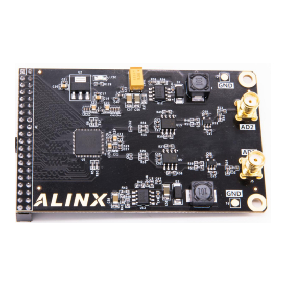
- Page 1 2-Channel High Speed AD Module AN8238 User Manual...
-
Page 2: Table Of Contents
Part 3: AD Sampling DEMO Program Description......... 10 Part 4: Hardware Connection and Testing............12 Part 4.1: Take the AX301B Development Board as an example..13 Part 4.2: Take the AX309 Development Board as an example.... 14 Part 4.3:Serial Display Voltage............... 16 2/17 www.alinx.com... -
Page 3: Part 1: 2-Channel High Speed Ad Module An9238
2-Channel High Speed AD Module AN9238 User Manual Part 1: 2-Channel High Speed AD Module AN9238 ALINX high-speed AD module AN9238 is a 2-channel 65MSPS, 12-bit analog signal to digital signal module. The AD conversion of the module adopts the AD9238 chip of ADI Company. The AD9238 chip supports 2-channel AD input conversion, so one AD9238 chip supports 2-channel AD input conversion. -
Page 4: Part 1.2: An9238 Module Size Dimension
Digital interface level standard: +3.3V CMOS level AD analog signal input range: -5V~+5V Analog signal input interface: SMA interface Measurement accuracy: about 10Mv Working temperature: -40°~85° Part 1.2: AN9238 Module Size Dimension Figure 1-2: AN9238 Module Size Dimension 4/17 www.alinx.com... -
Page 5: Part 2: An9238 Module Function Description
On the FPGA development board, the input voltage of -5V~+5V is reduced to -1V~+1V through the AD8065 chip and voltage divider resistors. If the user wants to input a wider range of voltage, just modify the resistance of the front-end voltage divider resistor. Conversion Formula: V = (1.0/5.02)*V 5/17 www.alinx.com... -
Page 6: Part 2.2: Single-Ended To Differential And Ad Conversion
Single-ended Differential Conversion The input voltage of -1V~+1V is converted into a differential signal (VIN+ − VIN−) by the AD8138 chip, and the common mode level of the differential signal is determined by the CML pin of AD. 6/17 www.alinx.com... -
Page 7: Part 2.4: Ad9238 Conversion
Amplifier Output (VIN+−VIN−) -5 V -1 V -1 V +5 V +1 V +1 V Part 2.4: AD9238 Conversion The default AD is configured as offset binary, and the value of AD conversion is shown in the figure below: 7/17 www.alinx.com... -
Page 8: Part 2.6: An9238 Digital Output Timing
The digital output of AD9238 dual-channel AD is +3.3VCMOS output mode, 2 channels (A and B) independent data and clock. AD data converts data on the rising and falling edges of the clock, and the FPGA end can sample the AD data with the AD clock. 8/17 www.alinx.com... -
Page 9: Part 2.7: The Pin Assignment Of An9238 Module
AD Channel A Data DATA0 CH1_D0 AD Channel A Data DATA3 CH1_D3 AD Channel A Data DATA2 CH1_D2 AD Channel A Data DATA5 CH1_D5 AD Channel A Data DATA4 CH1_D4 AD Channel A Data DATA7 CH1_D7 AD Channel A Data DATA6 CH1_D6 9/17 www.alinx.com... -
Page 10: Part 3: Ad Sampling Demo Program Description
AD data; the data conversion module volt_cal.v completes the voltage and hexadecimal to decimal format conversion; the serial port sending program uart.v completes the serial data transmission of the ASIC code of the collected data. 10/17 www.alinx.com... - Page 11 ASIC code. In the program, the serial port transmitting program and the serial port clock generation program are called, and the voltage value is transmit to the PC upper computer according to the baud rate of 9600. 11/17 www.alinx.com...
-
Page 12: Part 4: Hardware Connection And Testing
(AX301B/AX4010 connect to J1 port, AX309 connect to J3). The following is the hardware connection diagram of ALINX AX301B FPGA development board and AN9328: The FPGA development board is powered on, and the signal generator generates a positive wave of -5V~+5V with a frequency of 200Khz. -
Page 13: Part 4.1: Take The Ax301B Development Board As An Example
2-Channel High Speed AD Module AN9238 User Manual Part 4.1: Take the AX301B Development Board as an example Open “signaltap” Quartus software download “ad9238_test.sof” file. After downloading, run signaltap, the waveform interface will display a positive wave signal 13/17 www.alinx.com... -
Page 14: Part 4.2: Take The Ax309 Development Board As An Example
Here we can observe the signal in hexadecimal, set it to hexadecimal and display as follows. Part 4.2: Take the AX309 Development Board as an example The following is the hardware connection diagram of ALINX AX309 FPGA development board and AN9328: 14/17 www.alinx.com... - Page 15 Download the "ad9238_test.bit" file in the Impact software, then open the "chipscope" software, and open the "ad9238_test.cpj" project in the chipscope. Click the "Open Cable/Search JTAG Chain" button to connect to the FPGA development board Open the "Bus Plot" interface, and the waveform interface will display a sine 15/17 www.alinx.com...
-
Page 16: Part 4.3:Serial Display Voltage
In addition, we can see the converted voltage value through the serial port, and the baud rate of the serial port is set to 9600. For example, AD input DC voltage +3.3V, the display is as follows (different modules will have certain deviations). 16/17 www.alinx.com... - Page 17 2-Channel High Speed AD Module AN9238 User Manual When the DC voltage is changed to -3.3V, the display is as follows (different modules will have certain deviations). 17/17 www.alinx.com...
Need help?
Do you have a question about the AN8238 and is the answer not in the manual?
Questions and answers