Table of Contents
Advertisement
Quick Links
Advertisement
Table of Contents

Related Manuals for Alinx AC7Z100B


Summary of Contents for Alinx AC7Z100B
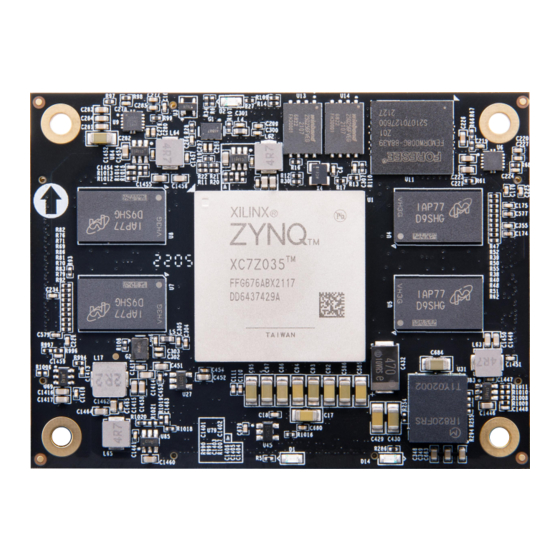
- Page 1 ZYNQ7000 FPGA Core Board AC7Z100B System on Module...
-
Page 2: Version Record
ZYNQ FPGA Core Board AC7Z100B User Manual Version Record Version Date Release By Description Rev 1.0 2020-06-28 Rachel Zhou First Release www.alinx.com 2 / 32... -
Page 3: Table Of Contents
Part 6: Clock Configuration ................17 Part 7: LED Light ..................20 Part 8: Reset circuit ..................21 Part 9: Power Supply ................. 22 Part 10: AC7Z100B Core Board Size Dimension ........24 Part 11: Board to Board Connectors Pin Assignment ....... 24 www.alinx.com 3 / 32... -
Page 4: Part 1: Ac7Z100B Core Board Introduction
ZYNQ FPGA Core Board AC7Z100B User Manual Part 1: AC7Z100B Core Board Introduction AC7Z100B (core board model, the same below) FPGA core board, ZYNQ chip is based on XC7Z100-2FFG900 of XILINX company ZYNQ7000 series. The ZYNQ chip's PS system integrates two ARM CortexTM-A9 processors, AMBA®... -
Page 5: Part 2: Zynq Chip
Figure 1-1: AC7Z100B Core Board (Front View) Figure 1-2: AC7Z100B Core Board (Rear View) Part 2: ZYNQ Chip The FPGA core board AC7Z100B uses Xilinx's Zynq7000 series chip, module XC7Z100-2FFG900. The chip's PS system integrates two ARM Cortex™-A9 processors, AMBA® interconnects, internal memory, external memory interfaces and peripherals. - Page 6 ZYNQ FPGA Core Board AC7Z100B User Manual interface, Ethernet interface, SD/SDIO interface, I2C bus interface, CAN bus interface, UART interface, GPIO etc. The PS can operate independently and start up at power on or reset. Figure 2-1 detailed the Overall Block Diagram of the ZYNQ7000 Chip.
- Page 7 ZYNQ FPGA Core Board AC7Z100B User Manual Two SD card, SDIO, MMC compatible controllers 2 SPIs, 2 UARTs, 2 I2C interfaces 54 multi-function IOs that can be configured as normal IO or peripheral control interfaces High bandwidth connection within PS and PS to PL The main parameters of the PL logic part are as follows: ...
-
Page 8: Part 3: Ddr3 Dram
ZYNQ FPGA Core Board AC7Z100B User Manual Figure 2-3: The XC7Z100 chip used on the Core Board Part 3: DDR3 DRAM The FPGA core board AC7Z100B is equipped with four Micron 512MB DDR3 chips, model MT41J256M16HA-125 (compatible with MT41K256M16HA-125), in which Two DDR3s are mounted on the PS and PL sides respectively. - Page 9 ZYNQ FPGA Core Board AC7Z100B User Manual U4,U5,U7,U8 MT41J256M16HA-125 256M x 16bit Micron Table 3-1: DDR3 SDRAM Configuration The hardware design of DDR3 requires strict consideration of signal integrity. We have fully considered the matching resistor/terminal resistance, trace impedance control, and trace length control in circuit design and PCB design to ensure high-speed and stable operation of DDR3.
- Page 10 ZYNQ FPGA Core Board AC7Z100B User Manual Figure 3-2: The Schematic Part of DDR3 DRAM on the PL side PS side DDR3 DRAM pin assignment: Signal Name ZYNQ Pin Name ZYNQ Pin Number PS_DDR3_DQS0_P PS_DDR_DQS_P0_502 PS_DDR3_DQS0_N PS_DDR_DQS_N0_502 PS_DDR3_DQS1_P PS_DDR_DQS_P1_502 PS_DDR3_DQS1_N...
- Page 11 ZYNQ FPGA Core Board AC7Z100B User Manual PS_DDR3_D20 PS_DDR_DQ20_502 PS_DDR3_D21 PS_DDR_DQ21_502 PS_DDR3_D22 PS_DDR_DQ22_502 PS_DDR3_D23 PS_DDR_DQ23_502 PS_DDR3_D24 PS_DDR_DQ24_502 PS_DDR3_D25 PS_DDR_DQ25_502 PS_DDR3_D26 PS_DDR_DQ26_502 PS_DDR3_D27 PS_DDR_DQ27_502 PS_DDR3_D28 PS_DDR_DQ28_502 PS_DDR3_D29 PS_DDR_DQ29_502 PS_DDR3_D30 PS_DDR_DQ30_502 PS_DDR3_D31 PS_DDR_DQ31_502 PS_DDR3_DM0 PS_DDR_DM0_502 PS_DDR3_DM1 PS_DDR_DM1_502 PS_DDR3_DM2 PS_DDR_DM2_502 PS_DDR3_DM3 PS_DDR_DM3_502 PS_DDR3_A0...
- Page 12 ZYNQ FPGA Core Board AC7Z100B User Manual PS_DDR3_BA2 PS_DDR_BA2_502 PS_DDR3_S0 PS_DDR_CS_B_502 PS_DDR3_RAS PS_DDR_RAS_B_502 PS_DDR3_CAS PS_DDR_CAS_B_502 PS_DDR3_WE PS_DDR_WE_B_502 PS_DDR3_ODT PS_DDR_ODT_502 PS_DDR3_RESET PS_DDR_DRST_B_502 PS_DDR3_CLK0_P PS_DDR_CKP_502 PS_DDR3_CLK0_N PS_DDR_CKN_502 PS_DDR3_CKE PS_DDR_CKE_502 PL side DDR3 DRAM pin assignment: Signal Name ZYNQ Pin Name ZYNQ Pin Number...
- Page 13 ZYNQ FPGA Core Board AC7Z100B User Manual PL_DDR3_D12 IO_L11N_T1_SRCC_33 PL_DDR3_D13 IO_L8P_T1_33 PL_DDR3_D14 IO_L11P_T1_SRCC_33 PL_DDR3_D15 IO_L10P_T1_33 PL_DDR3_D16 IO_L18P_T2_33 PL_DDR3_D17 IO_L14P_T2_SRCC_33 PL_DDR3_D18 IO_L14N_T2_SRCC_33 PL_DDR3_D19 IO_L13P_T2_MRCC_33 PL_DDR3_D20 IO_L16P_T2_33 PL_DDR3_D21 IO_L17P_T2_33 PL_DDR3_D22 IO_L16N_T2_33 PL_DDR3_D23 IO_L17N_T2_33 PL_DDR3_D24 IO_L23P_T3_33 PL_DDR3_D25 IO_L22N_T3_33 PL_DDR3_D26 IO_L19P_T3_33 PL_DDR3_D27 IO_L20N_T3_33 PL_DDR3_D28...
-
Page 14: Part 4: Qspi Flash
IO_L24P_T3_34 Part 4: QSPI Flash The FPGA core board AC7Z100B is equipped with two 256MBit Quad-SPI FLASH chips to form an 8-bit bandwidth data bus, the flash model is W25Q256FVEI, which uses the 3.3V CMOS voltage standard. Due to the non-volatile nature of QSPI FLASH, it can be used as a boot device for the system to store the boot image of the system. - Page 15 ZYNQ FPGA Core Board AC7Z100B User Manual section of the ZYNQ chip. In the system design, the GPIO port functions of these PS ports need to be configured as the QSPI FLASH interface. Figure 4-1 shows the QSPI Flash in the schematic.
-
Page 16: Part 5: Emmc Flash
ZYNQ FPGA Core Board AC7Z100B User Manual Part 5: eMMC Flash The FPGA core board AC7Z100B is equipped with a large-capacity 8GB eMMC FLASH chip, model THGBMFG6C1LBAIL, which supports the JEDEC e-MMC V5.0 standard HS-MMC interface with level support of 1.8V or 3.3V. -
Page 17: Part 6: Clock Configuration
ZYNQ FPGA Core Board AC7Z100B User Manual Pin Assignment of eMMC Flash Signal Name ZYNQ Pin Name ZYNQ Pin Number MMC_CCLK PS_MIO48_501 MMC_CMD PS_MIO47_501 MMC_D0 PS_MIO46_501 MMC_D1 PS_MIO49_501 MMC_D2 PS_MIO50_501 MMC_D3 PS_MIO51_501 Part 6: Clock Configuration The core system provides a reference clock for the PS system, the PL logic section, and the GTX transceiver, allowing the PS system and PL logic to work independently. - Page 18 The ZYNQ chip provides a 33.333MHz clock input to the PS section via the X4 crystal on the FPGA core board AC7Z100B. The input of the clock is connected to the pin of the PS_CLK_500 of the BANK500 of the ZYNQ chip.
- Page 19 SYS_CLK_P SYS_CLK_N GTX reference clock The FPGA core board AC7Z100B provides a 125Mhz reference clock for the GTX transceiver. The reference clock is connected to the reference clock input REFCLK1P/REFCLK1N of the BANK111. The schematic diagram of the clock source is shown in Figure 6-4.
-
Page 20: Part 7: Led Light
BANK111_CLK1_N Part 7: LED Light There are 2 red LED lights on the AC7Z100B FPGA core board, one of which is the power indicator light (PWR), one is the configuration LED light (DONE). When the core board is powered, the power indicator will illuminate;... -
Page 21: Part 8: Reset Circuit
Figure 7-1: AC7Z100B FPGA Core board LED light Hardware Connection Part 8: Reset circuit There is a reset circuit on the AC7Z100B core board. The reset input signal is connected to the reset button on the carrier board. The reset output is connected to the PS reset pin of the ZYNQ chip. -
Page 22: Part 9: Power Supply
PS_POR_B_500 ZYNQ system reset signal Part 9: Power Supply The AC7Z100B FPGA core board is powered by DC5V and is powered by a connection carrier board. The power supply design diagram on the FPGA board is shown in Figure 9-1 Figure 9-1:Power interface section in the schematic... - Page 23 ZYNQ FPGA Core Board AC7Z100B User Manual by DCDC chip ETA8156. The VTT and VREF voltages of the DDR3 of the PS section and the PL section are generated by U7, U10. In addition, the IO power supply BANK10 BANK11...
-
Page 24: Part 10: Ac7Z100B Core Board Size Dimension
ZYNQ FPGA Core Board AC7Z100B User Manual Part 10: AC7Z100B Core Board Size Dimension Figure 10-1: AC7Z100B Core Board Size Dimension Part Board Board Connectors Assignment The core board has a total of four high-speed expansion ports. It uses four 120-pin inter-board connectors (J29~J32) to connect to the carrier board. - Page 25 ZYNQ FPGA Core Board AC7Z100B User Manual ZYNQ Pin ZYNQ Pin J29 Pin Signal Name J29 Pin Signal Name Number Number B11_L4_N AJ24 B11_L1_N AK25 B11_L4_P AJ23 B11_L1_P AJ25 B11_L3_P AJ21 B11_L8_N AG25 B11_L3_N AK21 B11_L8_P AG24 B11_L2_N AK23 B11_L12_N...
- Page 26 ZYNQ FPGA Core Board AC7Z100B User Manual B10_L4_P AJ16 B10_L6_P AH17 B10_L4_N AK16 B10_L6_N AH16 B10_L16_P AE16 B10_L24_N AB16 B10_L16_N AE15 B10_L24_P AB17 B10_L20_P AA15 B10_L5_N AK15 B10_L20_N AA14 B10_L5_P AJ15 B10_L18_P AD16 B10_L23_P AC17 B10_L18_N AD15 B10_L23_N AC16 B10_L14_N...
- Page 27 ZYNQ FPGA Core Board AC7Z100B User Manual ZYNQ Pin ZYNQ Pin J30 Pin Signal Name J30 Pin Signal Name Number Number BANK111_TX0_N BANK111_RX0_N BANK111_TX0_P BANK111_RX0_P BANK111_TX1_N BANK111_RX1_N BANK111_TX1_P BANK111_RX1_P BANK111_TX2_N BANK111_RX2_N BANK111_TX2_P BANK111_RX2_P BANK111_TX3_N BANK111_RX3_N BANK111_TX3_P BANK111_RX3_P BANK111_CLK0_N BANK111_CLK1_N BANK111_CLK0_P...
- Page 28 ZYNQ FPGA Core Board AC7Z100B User Manual BANK109_RX2_N BANK110_RX0_N BANK109_RX2_P BANK110_RX0_P BANK109_RX3_N BANK110_TX0_N BANK109_RX3_P BANK110_TX0_P BANK109_RX1_P BANK110_RX1_N BANK109_RX1_N BANK110_RX1_P BANK109_TX1_P BANK110_TX1_N BANK109_TX1_N BANK110_TX1_P BANK109_TX2_P BANK110_RX2_N BANK109_TX2_N BANK110_RX2_P BANK109_TX3_P BANK110_TX2_N BANK109_TX3_N BANK110_TX2_P AA12 BANK109_TX0_N BANK110_RX3_N BANK109_TX0_P AK10 BANK110_RX3_P BANK109_RX0_N BANK110_TX3_N BANK109_RX0_P...
- Page 29 ZYNQ FPGA Core Board AC7Z100B User Manual ZYNQ Pin ZYNQ Pin J31 Pin Signal Name J31 Pin Signal Name Number Number FPGA_TCK FPGA_TDI FPGA_TMS FPGA_TDO B35_L2_P B35_L8_N B35_L2_N B35_L8_P B35_L9_P B35_L3_N B35_L9_N B35_L3_P B35_L22_N B35_L5_P B35_L22_P B35_L5_N B35_L20_N B35_L10_P B35_L20_P...
- Page 30 ZYNQ FPGA Core Board AC7Z100B User Manual B35_L18_N B35_L13_N B35_L18_P B35_L13_P B35_L15_N B35_L17_N B35_L15_P B35_L17_P B35_L7_N B35_L7_P B35_L6_N B35_L6_P SYS_RESET Pin assignment of J32 connector www.alinx.com 30 / 32...
- Page 31 ZYNQ FPGA Core Board AC7Z100B User Manual ZYNQ Pin ZYNQ Pin J32 Pin Signal Name J32 Pin Signal Name Number Number PS_MIO5 PS_MIO17 PS_MIO4 PS_MIO18 PS_MIO14 PS_MIO19 PS_MIO15 PS_MIO20 PS_MIO52 PS_MIO16 PS_MIO53 PS_MIO21 PS_MIO7 PS_MIO26 PS_MIO25 PS_MIO40 PS_MIO24 PS_MIO41 PS_MIO23...
- Page 32 ZYNQ FPGA Core Board AC7Z100B User Manual B12_L3_P PS_MIO28 B12_L3_N PS_MIO37 B12_L5_P AA27 PS_MIO38 B12_L5_N AA28 PS_MIO39 B12_L8_N AE30 B12_L21_P AJ28 B12_L8_P AD30 B12_L21_N AJ29 B12_L15_N AG29 B12_L7_N AD26 B12_L15_P AF29 B12_L7_P AC26 B11_L23_N AA23 B11_L11_P AD23 B11_L23_P AA22 B11_L11_N...
Need help?
Do you have a question about the AC7Z100B and is the answer not in the manual?
Questions and answers