Table of Contents
Advertisement
Quick Links
Advertisement
Table of Contents

Related Manuals for Alinx AC7010BB


Summary of Contents for Alinx AC7010BB
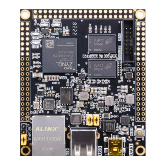
- Page 1 ZYNQ7000 FPGA Core Board AC7010BB/AC7020BB User Manual...
-
Page 2: Version Record
AC7010B / AC7020B User Manual Version Record Revision Date Release By Description Rev 1.0 2022-09-07 www.alinx.com 2 / 39... -
Page 3: Table Of Contents
Part 6.8: Reset Key ................30 Part 7:ZYNQ PL Peripherals ..............30 Part 7.1: User LEDs ................30 Part 7.2: Expansion Port J10 .............. 31 Part 7.3: Expansion Port J11 .............. 34 Part 7.4: Expansion Port J12 .............. 36 www.alinx.com 3 / 39... - Page 4 AC7010B / AC7020B User Manual The two core boards of the ALINX XILINX ZYNQ7000 development platform were officially released in 2022, models: AC7010B and AC7020B (industrial grade). Their development platform is the solution for XILINX's Zynq7000 SOC chip. It uses ARM+FPGA SOC technology to integrate dual-core ARM Cortex-A9 and FPGA programmable logic on a single chip.
-
Page 5: Part 1: Introduction
Zynq7000's XC7Z010-1CLG400C chip, and the AC7020B uses the Zynq7000's XC7Z020-2CLG400I chip, both of which are 400-pin FBGA packages. The ZYNQ7000 chip can be divided into a processor system part processor system (PS) and a programmable logic part Programmable Logic www.alinx.com 5 / 39... - Page 6 In addition, there is a 7 x 2 JTAG connector on the core board that can be downloaded and debugged via the ALINX Xilinx USB Cable Downloader. Figure 1-2 shows the structure of the entire AC7010B/AC7020B system:...
- Page 7 3-way 40-pin expansion port (0.1inch Spacing) 3-way 40-pin 0.1inch spacing expansion port for extending the IOs of ZYNQ PL and PL parts, and can be connect to various ALINX modules (binocular camera, TFT LCD screen, high-speed AD module, etc.) www.alinx.com...
-
Page 8: Part 2: Dimensional Structure
Power input: The core board supply voltage is DC5V. When the core board works alone, connect the USB cable to the USB port of the computer to supply power to the core board. When working with carrier board together, the core board also powered through carrier board. www.alinx.com 8 / 39... - Page 9 VCCIO34 is powered by the BANK34 of ZYNQ, and the VCCIO35 is powered by the BANK35 of ZYNQ. By replacing with other LDO chips, BANK34 and BANK35IO adapts to different voltage standards. +1.5V Generates VTT and VREF voltages required by DDR3 via TI's TPS51200 www.alinx.com 9 / 39...
-
Page 10: Part 4: Zynq Chip
Ethernet interface, SD/SDIO interface, I2C bus interface, CAN bus interface, UART interface, GPIO etc. The PS can operate independently and start up at power up or reset. Figure 4-1 detailed the Overall Block Diagram of the ZYNQ7000 Chip. www.alinx.com 10 / 39... - Page 11 Two SD card, SDIO, MMC compatible controllers 2 SPIs, 2 UARTs, 2 I2C interfaces 4 sets of 32bit GPIO, 54 (32+22) as PS system IO, 64 connected to PL High bandwidth connection within PS and PS to PL www.alinx.com 11 / 39...
- Page 12 + number, which represents the pin of the BGA. Figure 4-2 detailed the XC7Z010 chip on the Core Board AC7010B. Figure 4-2: The XC7Z010 chip on the Core Board AC7010B www.alinx.com 12 / 39...
-
Page 13: Part 4.1: Jtag Interface
First, let's talk about the JTAG debug interface (J14) of the AC7010B/AC7020B core board. Users can debug and download the ZYNQ program by connecting the ALINX Xilinx USB Cable downloader. Figure 4-3 shows the schematic part of the JTAG port, which involves four signals, TCK, TMS, TDO, and TDI. -
Page 14: Part 4.3: Zynq Boot Configuration
VCCBRAM have the same voltage, they can be powered up at the same time. The order of power outages is reversed. Part 4.3: ZYNQ boot configuration The AC7010B/AC7020B FPGA Core board supports three boot modes. The three boot modes are JTAG debug mode, QSPI FLASH and SD card boot www.alinx.com 14 / 39... -
Page 15: Part 5: Clock Configuration
X1 crystal on the FPGA core board. The input of the clock is connected to the pin of the PS_CLK_500 of the BANK500 of the ZYNQ chip. The schematic diagram is shown in Figure 5-1: Figure 5-1: Active crystal oscillator to the PS section www.alinx.com 15 / 39... -
Page 16: Part 5.2: Pl System Clock Source
FPGA logic. Some peripherals on the FPGA core board are connected to the IO of the PS, and some peripherals are connected to the IO of the PL. First introduce the peripherals connected to the PS part. www.alinx.com 16 / 39... -
Page 17: Part 6.1: Qspi Flash
ZYNQ chip. In the system design, the GPIO port functions of these PS ports need to be configured as the QSPI FLASH interface. Figure 6-1 shows the QSPI Flash in the schematic. Figure 6-1: QSPI Flash Connection Diagram www.alinx.com 17 / 39... -
Page 18: Part 6.2: Ddr3 Dram
ZYNQ Pin Number QSPI_SCK PS_MIO6_500 QSPI_CS PS_MIO1_500 QSPI_D0 PS_MIO2_500 QSPI_D1 PS_MIO3_500 QSPI_D2 PS_MIO4_500 QSPI_D3 PS_MIO5_500 Part 6.2: DDR3 DRAM The AC7010B FPGA core board is equipped with two SKHynix 2Gbit DDR3 chips (total 4Gbit), model H5TQ2G63FFR-RDC (compatible with www.alinx.com 18 / 39... - Page 19 The hardware design of DDR3 requires strict consideration of signal integrity. We have fully considered the matching resistor/terminal resistance, trace impedance control, and trace length control in circuit design and PCB design to ensure high-speed and stable operation of DDR3. www.alinx.com 19 / 39...
- Page 20 ZYNQ Pin Name ZYNQ Pin Number DDR3_DQS0_P PS_DDR_DQS_P0_502 DDR3_DQS0_N PS_DDR_DQS_N0_502 DDR3_DQS1_P PS_DDR_DQS_P1_502 DDR3_DQS1_N PS_DDR_DQS_N1_502 DDR3_DQS2_P PS_DDR_DQS_P2_502 DDR3_DQS2_N PS_DDR_DQS_N2_502 DDR3_DQS3_P PS_DDR_DQS_P3_502 DDR3_DQS4_N PS_DDR_DQS_N3_502 DDR3_DQ[0] PS_DDR_DQ0_502 DDR3_DQ [1] PS_DDR_DQ1_502 DDR3_DQ [2] PS_DDR_DQ2_502 DDR3_DQ [3] PS_DDR_DQ3_502 DDR3_DQ [4] PS_DDR_DQ4_502 www.alinx.com 20 / 39...
- Page 21 DDR3_DQ [26] PS_DDR_DQ26_502 DDR3_DQ [27] PS_DDR_DQ27_502 DDR3_DQ [28] PS_DDR_DQ28_502 DDR3_DQ [29] PS_DDR_DQ29_502 DDR3_DQ [30] PS_DDR_DQ30_502 DDR3_DQ [31] PS_DDR_DQ31_502 DDR3_DM0 PS_DDR_DM0_502 DDR3_DM1 PS_DDR_DM1_502 DDR3_DM2 PS_DDR_DM2_502 DDR3_DM3 PS_DDR_DM3_502 DDR3_A[0] PS_DDR_A0_502 DDR3_A[1] PS_DDR_A1_502 DDR3_A[2] PS_DDR_A2_502 DDR3_A[3] PS_DDR_A3_502 DDR3_A[4] PS_DDR_A4_502 www.alinx.com 21 / 39...
-
Page 22: Part 6.3: Gigabit Ethernet Interface
Zynq7000 PS system through the RGMII interface. JL2121-N040I supports MDI/MDX adaptation, various speed self-adjustment, Master/Slave adaptation, and supports MDIO bus for PHY register management. The JL2121-N040I power-on will detect the level status of some specific IOs to determine their working mode. www.alinx.com 22 / 39... - Page 23 ZYNQ and PHY chip JL2121-N040I is communicated through RMII bus, and the transmission clock is 25Mhz. Data is sampled on the rising edge and falling samples of the clock. Figure 6-4: The connection of the ZYNQ and GPHY chip www.alinx.com 23 / 39...
-
Page 24: Part 6.4: Usb2.0 Interface
Type A) and a micro USB interface (Micro USB), which are convenient for users to connect different USB peripherals. Users can switch between Host and OTG through J5 and J6 jumpers on the core board. Table 6-3 shows the www.alinx.com 24 / 39... - Page 25 Figure 6-7 shows the physical diagram of the USB2.0 part. U11 is USB3320C, J3 is the Host USB interface, and J4 is the OTG USB interface. Jumper caps J5 and J6 are used for Host and OTG mode selection. www.alinx.com 25 / 39...
-
Page 26: Part 6.5: Usb To Serial Port
BANK501 of the ZYNQ EPP. Since the VCCMIO of the BANK is set to 1.8V, the data level of the CP2102GM is 3.3V, which is connected by the TXS0102DCUR level conversion chip. Figure 6-8 detailed the schematic diagram of the CP2102GM and ZYNQ connections www.alinx.com 26 / 39... - Page 27 Uart data output Silicon Labs provides virtual COM port (VCP) drivers for host PCs. These drivers allow the CP2102GM USB-UART bridge device to be displayed as a COM port in communications application software, such as TeraTerm or www.alinx.com 27 / 39...
-
Page 28: Part 6.6: Sd Card Slot
SD card is 3.3V, connected through the TXS02612 level shifter. The schematic of the Zynq7000 PS and SD card connector is shown in Figure 6-10: Figure 6-10: SD Card Connection Diagram Figure 6-11: SD Card Slot on the FPGA Board www.alinx.com 28 / 39... -
Page 29: Part 6.7: User Leds
BANK500 IO voltage is low, the LED will be illuminated. Figure 6-14 shows the connection between ZYNQ BANK500 IO and LED lights. Figure 6-12: Zynq-7000 and LED connection diagram Figure 6-13: PS User LEDs on the FPGA Core Board www.alinx.com 29 / 39... -
Page 30: Part 6.8: Reset Key
PS Reset Key Part 7:ZYNQ PL Peripherals Part 7.1: User LEDs The PL part of the AC7010B/AC7020B FPGA core board is also connected to one LED light-emitting diode. The schematic diagram is shown in Figure 7-1, www.alinx.com 30 / 39... -
Page 31: Part 7.2: Expansion Port J10
Description LED2 IO_0_34 PL User LED PL LED2 Part 7.2: Expansion Port J10 The expansion port J10 is a 40-pin 2.54mm double-row connector, which expands more peripherals and interfaces for users. The default is not soldered, www.alinx.com 31 / 39... - Page 32 Do not directly connect the IO directly to the 5V device to avoid burning the FPGA. If you want to connect 5V equipment, you need to connect level conversion chip. The circuit of the expansion port (J10) is shown in Figure 7-3: Figure 7-3: Expansion header J10 schematic www.alinx.com 32 / 39...
- Page 33 PIN15 IO34_L11P PIN16 IO34_L11N PIN17 IO34_L6P PIN18 IO34_L6N PIN19 IO34_L5N PIN20 IO34_L5P PIN21 IO34_L3N PIN22 IO34_L3P PIN23 IO34_L4P PIN24 IO34_L4N PIN25 IO34_L2N PIN26 IO34_L2P PIN27 IO34_L1N PIN28 IO34_L1P PIN29 PS_MIO9 PIN30 PS_MIO14 PIN31 PS_MIO11 PIN32 PS_MIO8 www.alinx.com 33 / 39...
-
Page 34: Part 7.3: Expansion Port J11
The expansion port J11, which expands more peripherals and interfaces for users. Currently, the J11 interface can be directly connected to the module provided by ALINX, include: ADDA module, LCD module, Gigabit Ethernet module, audio input/output module, matrix keyboard module, 500W binocular vision camera module, etc. - Page 35 J11 Expansion Header Pin Assignment J11 Pin Signal Name ZYNQ Pin Number PIN1 PIN2 PIN3 IO34_L23P PIN4 IO34_L23N PIN5 IO34_L24P PIN6 IO34_L24N PIN7 IO35_L9N PIN8 IO35_L9P PIN9 IO35_L7N PIN10 IO35_L7P PIN11 IO34_L20P PIN12 IO34_L20N PIN13 IO34_L15N www.alinx.com 35 / 39...
-
Page 36: Part 7.4: Expansion Port J12
The default is not soldered, the user can solder to a double-row male connectors or female connectors as needed. The J12 interface can be directly connected to the module provided by ALINX. The expansion port J12, which expands more peripherals and www.alinx.com... - Page 37 AC7010B / AC7020B User Manual interfaces for users. Currently, the J12 interface can be directly connected to the module provided by ALINX, include: ADDA module, LCD module, Gigabit Ethernet module, audio input/output module, matrix keyboard module, 500W binocular vision camera module, etc.
- Page 38 PIN17 IO35_L13P PIN18 IO35_L13N PIN19 IO35_L10N PIN20 IO35_L10P PIN21 IO35_L19P PIN22 IO35_L19N PIN23 IO35_L20P PIN24 IO35_L20N PIN25 IO35_L8P PIN26 IO35_L8N PIN27 IO35_L2P PIN28 IO35_L2N PIN29 PS_MIO9 PIN30 PS_MIO14 PIN31 PS_MIO11 PIN32 PS_MIO8 PIN33 PS_MIO13 PIN34 PS_MIO15 www.alinx.com 38 / 39...
- Page 39 AC7010B / AC7020B User Manual PIN35 PS_MIO10 PIN36 PS_MIO12 PIN37 PIN38 PIN39 +3.3V PIN40 +3.3V www.alinx.com 39 / 39...
Need help?
Do you have a question about the AC7010BB and is the answer not in the manual?
Questions and answers