
Subscribe to Our Youtube Channel
Related Manuals for Aiwa AM-F90


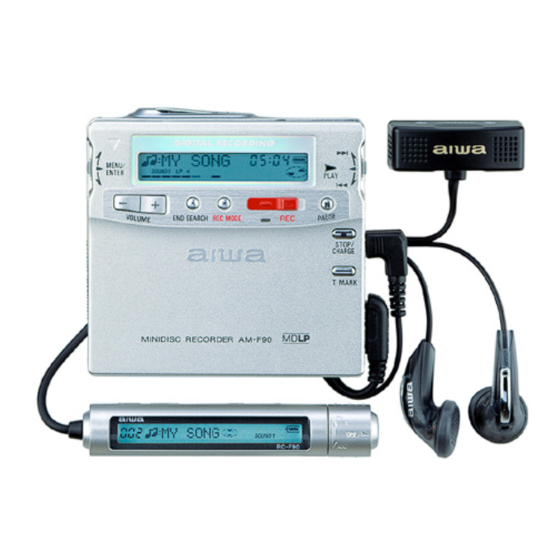
Summary of Contents for Aiwa AM-F90
- Page 1 AM-F90 AHK1 (S) SERVICE MANUAL MINIDISC RECORDER BASIC MD MECHANISM : MT-MZR900-171 S/M Code No. 09-01A-355-4N2...
-
Page 2: Table Of Contents
TABLE OF CONTENTS SPECIFICATIONS .............................. 3 ACCESSORIES/PACKAGE LIST-1/1 ......................... 4 PROTECTION OF EYES FROM LASER BEAM DURING SERVICING ............5 Optical Pickup Block and Base Unit Handling Precautions ................. 6 Service Note ................................ 7 DISASSEMBLY INSTRUCTIONS ........................8-13 ELECTRICAL MAIN PARTS LIST ....................... 14-17 BLOCK DIAGRAM-1/3 (SERVO) ........................ -
Page 3: Specifications
SPECIFICATIONS • Design and specifications are subject to change without notice. • Dolby noise reduction and HX Pro headroom extension manufactured under license from Dolby Laboratories Licensing Corporation. HX Pro originated by Bang & Olufsen. “DOLBY”, the double-D symbol and “HX PRO” are trademarks of Dolby Laboratories Licensing Corporation. -
Page 4: Accessories/Package List-1/1
ACCESSORIES/PACKAGE LIST-1/1 REF. NO PART NO. KANRI DESCRIPTION 1 8B-HM1-902-010 IB,HK(ECH) 2 8B-HM1-951-010 RC UNIT,RC-F90 3 87-B30-138-010 MIC,CM-MS001 4 87-B30-491-010 HEADPHONE,HP-M041(S) S-G 5 91-251-895-110 CASE,BAT UM-3 6 91-EM0-003-110 AC ADAPTOR,AMF90EX 7 91-756-120-110 BAT,NH-14WM(A) 8 93-043-060-010 CASE,BAT 9 93-220-749-010 CARRYNG,CASE 10 9X-337-932-120 CASE ASSY,BAT 11 91-EM0-007-110 OPTICAL CABLE... -
Page 5: Protection Of Eyes From Laser Beam During Servicing
PROTECTION OF EYES FROM LASER BEAM DURING SERVICING This set employs laser. Therefore, be sure to follow carefully the CAUTION instructions below when servicing. Use of controls or adjustments or performance of procedures other than those specified herein may result in hazardous WARNING! radiation exposure. -
Page 6: Optical Pickup Block And Base Unit Handling Precautions
Optical Pickup Block and Base Unit Handling Precautions (LCX-4R) The laser diode inside the optical pickup can be destroyed by • If the MAIN C.B is removed when this machine is powered static electricity due to the static charge accumulated in human on during repair, this machine will not work. -
Page 7: Service Note
Service Note • The sets that use the microprocessor version 1.000 are adjusted of their setup data by the MANUAL mode in the factory before shipment. If the NV reset is executed in these sets, the setup data will be cleared. If the NV reset is executed in the sets of version 1.000, change the adjustment value in accordance with the adjustment value change procedure immediately after... -
Page 8: Disassembly Instructions
DISASSEMBLY INSTRUCTIONS-1/6 If the numbers such as 1 are shown in the illustration, disassemble the machine in the numerical order given in the illustration. PANEL, BOTTOM S801 Note : S802 When re-assembling, align the position of the KNOB, HOLD and that of the switches (S801, S802). - Page 9 DISASSEMBLY INSTRUCTIONS-2/6 LCD MODULE and PANEL, TOP 1 Five tapping screws (1.7) 2 LCD MODULE 3 PANEL, TOP MAIN C.B ASSY 6 Connector (CN501). 1 Remove soldering at the two points on the FLEX C.B (Overwrite head). 7 MAIN C.B ASSY. 3 Four toothed machine screws (M1.4).
- Page 10 DISASSEMBLY INSTRUCTIONS-3/6 BATTERY CASE ASSY, MAIN C.B 2 BATTERY CASE ASSY. 3 MAIN C.B . 1 Remove soldering of the battery terminal (+). 1 Remove soldering of the battery terminal (-). CENTER FRAME ASSY 1 Pull in the direction of the arrow A and disengage 5 Remove the CENTER FRAME ASSY in the direction of the arrow C.
- Page 11 DISASSEMBLY INSTRUCTIONS-4/6 MD MECHANISM DECK (MT-MZR900-171), CHASSIS ASSY 2 Protruded ( ) portion 3 MD MECHANISM DECK (MT-MZR900-171) 2 Protruded ( ) portion 4 Tension coil spring (arm). 1 Screw ( 1.4) 5 CHASSIS ASSY 1 Screw ( 1.4) REPAIR OP ASSY (LCX-4R) 2 GEAR (SA) 6 Screw for precision 1 Washer...
- Page 12 DISASSEMBLY INSTRUCTIONS-5/6 HOLDER ASSY 5 Remove the HOLDER ASSY in the direction of the arrow D. 2 Push the protruded ( ) portion in the direction of the arrow B and open the HOLDER ASSY in the direction of the arrow A. 1 Open the HOLDER ASSY.
- Page 13 DISASSEMBLY INSTRUCTIONS-6/6 DC motor (sled) (M602) 1 Remove soldering at the four locations of the MOTOR FLEX C.B. 2 Washer (0.8-2.5) 4 Two precision screws (M1.4) 3 GEAR (SA) 5 DC motor (sled) (M602) DC motor (spindle) (M601), DC motor (overwrite head OWH UP/DOWN) (M603) 1 Remove soldering at the six locations Note: of the MOTOR FLEX C.B.
-
Page 14: Electrical Main Parts List
ELECTRICAL MAIN PARTS LIST-1/4 REF. NO PART NO. KANRI DESCRIPTION REF. NO PART NO. KANRI DESCRIPTION MAIN C.B C511 91-164-850-810 C-CAP,CER 10P-16 C512 91-125-777-810 C-CAP,CER 0.1-10 C101 91-125-837-910 C-CAP,CER 1-6.3 C513 91-164-850-810 C-CAP,CER 10P-16 C103 91-125-837-910 C-CAP,CER 1-6.3 C514 91-107-819-810 C-CAP,CER 0.022-16 C104 91-135-868-910... - Page 15 ELECTRICAL MAIN PARTS LIST-2/4 REF. NO PART NO. KANRI DESCRIPTION REF. NO PART NO. KANRI DESCRIPTION C818 91-125-777-810 C-CAP,CER 0.1-10 IC301 98-759-829-440 IC,AK4562VN-L C819 91-127-772-810 C-CAP,CER 0.033-10 IC302 98-759-829-770 IC,AN7536FHNEBV C820 91-127-772-810 C-CAP,CER 0.033-10 IC303 98-759-699-540 IC,NJM2173APC1 C821 91-127-895-910 C-CAP,TN 22-4 IC501 98-759-689-670 IC,SN761057DBT...
- Page 16 ELECTRICAL MAIN PARTS LIST-3/4 REF. NO PART NO. KANRI DESCRIPTION REF. NO PART NO. KANRI DESCRIPTION R507 91-218-953-810 C-RES,1K-1/16 R831 91-218-990-810 C-RES,0-1/16 R517 91-208-895-810 C-RES,2.2K-1/16-0.5 R832 91-218-990-810 C-RES,0-1/16 R519 91-218-977-810 C-RES,100K-1/16 R833 91-218-990-810 C-RES,0-1/16 R521 91-218-446-910 C-RES,1-1/16 R834 91-218-990-810 C-RES,0-1/16 R601 91-218-989-810 C-RES,1M-1/16...
- Page 17 ELECTRICAL MAIN PARTS LIST-4/4 • Regarding connectors, they are not stocked as they are not the initial order items. The connectors are available after they are supplied from connector manufacturers upon the order is received. CHIP RESISTOR PART CODE Chip Resistor Part Coding Figure Resistor Code Value of resistor...
-
Page 18: Block Diagram-1/3 (Servo)
BLOCK DIAGRAM-1/3 (SERVO) OVER WRITE HEAD DRIVE IC601 (1/2) SIGNAL PATH HR601 : PLAY BACK OVER WRITE OVER HEAD DRIVE OPTICAL PICK-UP BLOCK PRE DRIVER WRITE : REC (ANALOG IN) Q604, 605 (LCX-4R) HEAD : REC (DIGITAL IN) OUTA VRECIN2 VRECO H-BRIDGE M603... -
Page 19: Block Diagram-2/3 (Audio)
BLOCK DIAGRAM-2/3 (AUDIO) OPTICAL RECEIVER B+ SWITCH VIF B+ Q302 DIN1 J301 LINE IN (OPT) (LINE IN JACK) MIC AMP IC303 J303 LIN2 OUT2 LIN1 (PLUG IN POWER) ADDT GAIN SDTO CONVERTER & RIN2 OUT1 RIN1 STBY REGULATOR A/D, D/A CONVERTER AUDIO IC301... -
Page 20: Block Diagram-3/3 (Display/Key Control/Power)
BLOCK DIAGRAM-3/3 (DISPLAY/KEY CONTROL/POWER) RMC KEY VRMC HEADPHONE AMP (IC302), XWK3 MOTOR/COIL DRIVER (IC551) RMC KEY CLK SEL CLK SEL FFCLR FFCLR SLEEP SLEEP SYSTEM VLON CONTROL VLON XWK1 POWER CONTROL WK DET XWK2 IC901 REC KEY XWK4 HALF LOCK SW VAIFON S805 OPEN... -
Page 21: Wiring-1/1
WIRING-1/1 MAIN C.B (CONDUCTOR SIDE ) RECHARGEBL BATTERY (NICKEL-METAL) S803 NH-14WM (A) PROTECT 1.2V 1400mAh DETECT MOTOR FLEXIBLE S805 MECHANISM OPEN MAIN C.B (COMPONENT SIDE) S802 S801 SYNCHRO REC HOLD ON T HOLD R317 C211 S804 BATTERY IN C811 J301(1/2) L802 DETECT R840... -
Page 22: Schematic Diagram-1/1
SCHEMATIC DIAGRAM-1/1 NH-14WM (A) -22-... -
Page 23: Wave Form
WAVE FORM-1/3 1 IC501 8 (IY) (PLAYBACK MODE) 5 IC501 1 (TE) (PLAYBACK MODE) 100 mV/DIV, 1 µs/DIV 20 mV/DIV, 500 ns/DIV Approx. Approx. 200 mVp-p 35 mVp-p (PLAYBACK MODE) 6 IC501 ‹ (RF OUT) (PLAYBACK MODE) 2 IC501 9 (IX) 100 mV/DIV, 1 µs/DIV 500 mV/DIV, 500 ns/DIV Approx. - Page 24 WAVE FORM-2/3 9 IC801 ∞ (OSCO) # IC801 (LRCK) 1 V/DIV, 10 µs/DIV 200 mV/DIV, 10 ns/DIV 2.5 Vp-p 1 Vp-p 22.8 µs 22.1 ns 0 IC801 ‡ (RFI) (PLAYBACK MODE) $ IC801 (XBCK) 500 mV/DIV, 500 ns/DIV 1 V/DIV, 200 ns/DIV Approx.
- Page 25 WAVE FORM-3/3 & IC301 ) (LRCK) ( IC301 & (BCLK) 1 V/DIV, 10 µs/DIV 1 V/DIV, 200 ns/DIV 2.5 Vp-p 2.5 Vp-p 22.8 µs 352 ns * IC301 ( (MCLK) ) IC901 (CLK) 500 mV/DIV, 2 µ s/DIV 1 V/DIV, 50 ns/DIV 1 Vp-p 2.5 Vp-p 5.68 µs...
- Page 26 TEST MODE-1/6 Introduction Operations in the Test Mode • The test mode consists of the two modes. One is the AUTO Adj. • When the machine enters the test mode, the machine enters further Mode and the other is the MANUAL Mode. the display check mode of the test mode.
- Page 27 TEST MODE-2/6 Configuration of the Test Mode MANUAL Mode. In the MANUAL Mode, movement of the machine is separated by Test mode (Display check mode). functions so that adjustment and operation check can be performed in Press the key. each movement. However, do not perform any adjustment using the MANUAL Mode MANUAL Mode.
- Page 28 TEST MODE-3/6 Each time the “JOG lever (left) £ ” (top) key or the Self-Diagnosis Result Display Mode “DISPLAY” key of remote control is pressed, the display This machine contains the Self-Diagnosis Result Display Mode. If an changes in the following order. error occurs during recording or playback, the mechanism control block of the microprocessor and the power supply control block detect the error status.
- Page 29 TEST MODE-4/6 To exit the Self-Diagnosis Result Display Mode and to return to the test mode (display check mode), press the “9” key. • Contents of the error display codes Simplified Contents of the error Display code Meaning of code Description contents display No error...
- Page 30 TEST MODE-5/6 Clearing the error display code When the “2” key is pressed, the total error counter is displayed on LCD. Each time the “§” key is pressed, the When all of the repair works are completed, clear the error display display advances to the next display s shown below.
- Page 31 TEST MODE-6/6 Key Check Mode When all keys of the main unit and of the remote control are confirmed to be OK, the following display appears for 4 The keys (including slide switch) of the main unit and of the remote seconds.
- Page 32 ELECTRICAL ADJUSTMENT-1/11 Introduction NV Reset • All electrical adjustments consisting of the CD adjustments, MO Note : The sets that use the microprocessor version 1.000 are adjustments and electrical offset adjustment are automatically adjusted of their setup data by the MANUAL mode in the performed when the machine enters the AUTO Adj.
- Page 33 ELECTRICAL ADJUSTMENT-2/11 4. Press the “JOG lever (left) ≤ ”(bottom) key or the “PLAY 4) Enter the MANUAL Mode of the test mode. Select the item number 862. (Refer to TEST MODE on page 27.) MODE” key of remote control. Display on remote control LCD (When the “JOG lever (left) ≤...
-
Page 34: Test Mode
ELECTRICAL ADJUSTMENT-3/11 • Vl PWM Duty (Item number : 764) Adjustment Method Check method : Display on remote control LCD 1. Enter the MANUAL Mode of the test mode and select the Laser Power Adjustment Mode (Item number : 010). (Refer to TEST MODE on page 27.) Display on remote control LCD : Adjustment value... - Page 35 ELECTRICAL ADJUSTMENT-4/11 AUTO Adj. Mode – MAIN C.B (Pattern side) – • Structure and flow of the AUTO Adj. Mode AUTO Adj. Mode Protect switch is ON CD Auto Adj. is NG item is detected in progress or the AP912 (GND) AP914 (VC) All items are OK AP915 (VL)
- Page 36 ELECTRICAL ADJUSTMENT-5/11 • Electrical Offset Adjustment Method 3. If the CD AUTO Adj. ends with NG, perform the NV Reset (refer to ELECTRICAL ADJUSTMENT on page 32). After that, Note: Be sure to perform the Electrical Offset Adjustment while perform the Temperature Compensation (refer to any disc is not inserted.
- Page 37 ELECTRICAL ADJUSTMENT-6/11 Clearing RESUME • CD AUTO Adjustment Items / MO AUTO Adjustment Items 1. CD AUTO Adjustment Items When all adjustments are completed, clear the RESUME as follows. Item number Contents • How to clear the RESUME 1. Enter the MANUAL Mode of the test mode. Select the item CD Electrical Offset Adjustment number 043.
- Page 38 ELECTRICAL ADJUSTMENT-7/11 5. Press the “DISPLAY” key of the remote control for several 16. Press the “VOL +” key once and change the value of the seconds (approx. 3 seconds) in order to enter the patch data flashing segments to 0D5F. Display on remote control LCD write mode.
- Page 39 ELECTRICAL ADJUSTMENT-8/11 28. Press the “VOL +” key once and change the value of the • How to write the modification data (for the microprocessor of flashing segments to 0D62. version 1.100). Display on remote control LCD 1. Enter the MANUAL Mode of the test mode. Select the item number 022.
- Page 40 ELECTRICAL ADJUSTMENT-9/11 13. Press the “VOL +” key (adjustment value increases) and/or the 25. Press the “VOL +” key (adjustment value increases) and/or the “VOL –” key (adjustment value dcreases) so that the “VOL –” key (adjustment value dcreases) so that the adjustment value becomes 04.
- Page 41 ELECTRICAL ADJUSTMENT-10/11 37. Press the “VOL +” key (adjustment value increases) and/or the 49. Press the “VOL +” key (adjustment value increases) and/or the “VOL –” key (adjustment value decreases) so that the “VOL –” key (adjustment value decreases) so that the adjustment value becomes 09.
- Page 42 ELECTRICAL ADJUSTMENT-11/11 61. Press the “VOL +” key (adjustment value increases) and/or the 73. Press the “VOL +” key (adjustment value increases) and/or the “VOL –” key (adjustment value decreases) so that the “VOL –” key (adjustment value dcreases) so that the adjustment value becomes F8.
-
Page 43: Ic Block Diagram
IC BLOCK DIAGRAM-1/3 IC, AK4562VN-L IC, AN7536FHNEBV 19 18 HEADPHONE /LINE MUTE BEEP CLOCK CONTROL CCLK DIVIDER REGISTER ROUT – AUDIO I/F R IN CONTROLLER DGND LOUT1 A/D CONVERTER /HPF L OUT L IN OPGAL VREF – ROUT1 GAIN GAIN AGND GAIN GA L... - Page 44 IC BLOCK DIAGRAM-2/3 IC, SC111257FCR2 42 41 – VC VG – PRE DRIVER PRE DRIVER PGNDW H-BRIDGE H-BRIDGE CONTROL CONTROL VMVW PGNDUV GND2 GND1 BIAS CPWI – PWM24 CPVI – CPUI – H-BRIDGE H-BRIDGE CPWO CONTROL CONTROL CPVO VC VG PRE DRIVER PRE DRIVER 3PHASE...
- Page 45 IC BLOCK DIAGRAM-3/3 XPC18A32FCR2 36 35 34 33 32 31 30 29 OUTPUT OUTPUT SW SERIES PASS SERIES PASS SERIES PASS OUTPUT SW REGULATOR VA REGULATOR VD REGULATOR VIF POWER – SWITCH 1 INM1 STEP-UP PRE DRIVER DTC1 XRST OUTPUT SW CRST DTC2 RSTREF...
-
Page 46: Ic Description-1/2 (Cxa1782Bq)-1/1
IC DESCRIPTION-1/2 (SN761057DBT)-1/1 Pin No. Pin Name Description Tracking error signal output to system controller (IC801). REXT — Terminal to which resistor for ADIP amplifier control is externally connected. WPPLPF — Terminal to which capacitor for TPP/WPP low-pass filter is externally connected. VREF11 Reference voltage output terminal. -
Page 47: Ic Description-2/2 (Cxd2671-203Gacxd2671-203 Ga)
IC DESCRIPTION-2/2 (CXD2671-203GA)-1/6 Pin No. Pin Name Description PAUSE KEY Main units' key input terminal (key input). Microphone sense signal output to the microphone amplifier (IC303). MIC SENSE “H”: HIGH, “L”: LOW, Normally: “H”. XTEST Input terminal for setting the test mode. “L”: Test mode. (Normally set to “H”). 4, 5 Not used in this machine. - Page 48 IC DESCRIPTION-2/2 (CXD2671-203GA)-2/6 Pin No. Pin Name Description FILI Filter input for master clock of playback EFM system master PLL. FILO Filter output of master clock from playback EFM system master PLL. CLTV Internal VCO control voltage input for playback EFM system master PLL. PEAK Peak hold signal input of laser light volume signal (RF/ABCD) from RF amplifier (IC501).
- Page 49 IC DESCRIPTION-2/2 (CXD2671-203GA)-3/6 Pin No. Pin Name Description DIFVSS0 — GND terminal (For DSP I/F). APCREF Control signal output to reference voltage generator circuit used for laser power automatic control. PWM signal output for laser power automatic control. Not used in this machine. (No connection LDDR terminal).
- Page 50 IC DESCRIPTION-2/2 (CXD2671-203GA)-4/6 Pin No. Pin Name Description DRAMVSS0 — GND terminal. (For external D-RAM). DRAMVDD0 — Power supply terminal. (For external D-RAM). (+2.4V). 120-138 Output terminal for external D-RAM. Not used in this machine. (No connection terminal). DRAMVDD1 — Power supply terminal.
- Page 51 IC DESCRIPTION-2/2 (CXD2671-203GA)-5/6 Pin No. Pin Name Description Serial data output to non-volatile memory (IC804), A/D, D/A converter (IC301) and LCD element module. Serial clock signal output to non-volatile memory (IC804), A/D, D/A converter (IC301) and SCK0 LCD element module. XGUM ON Charging battery pack detector switch (S804) input terminal.
- Page 52 IC DESCRIPTION-2/2 (CXD2671-203GA)-6/6 Pin No. Pin Name Description XRF RST Reset control signal output to RF amplifier (IC501). MCUVDD3 — Power supply terminal (for microprocessor block) (+1.5V). SPDL MON Spindle servo monitor signal input from motor driver (IC551). 224-226 Not used in this machine. (No connection terminal) XHOLD SW HOLD switch (S801) input terminal.
-
Page 53: Mechanical Exploded View-1/3 (Main Unit)
MECHANICAL EXPLODED VIEW-1/3 (MAIN UNIT) -53-... -
Page 54: Mechanical Exploded View-2/3 (Main C.b Block)
MECHANICAL EXPLODED VIEW-2/3 (MAIN C.B BLOCK) not supplied -54-... -
Page 55: Mechanical Exploded View-3/3 (Md Mechanism Deck)
MECHANICAL EXPLODED VIEW-3/3 (MD MECHANISM DECK) M603 not supplied M602 -55-... -
Page 56: Mechanical Parts List-1/1
MECHANICAL PARTS LIST-1/1 REF. NO PART NO. KANRI DESCRIPTION REF. NO PART NO. KANRI DESCRIPTION 1 8B-HM1-001-010 PANEL ASSY,TOP 70 93-226-168-010 SPACER,REAR 2 94-218-229-090 SCREW,M1.4-T 71 93-225-171-010 SH,CLV 3 8B-HM1-005-010 KNOB,SL REC 72 93-220-472-010 SPR-E OPEN 4 8B-HM1-004-010 KEY,CONT 73 94-223-088-010 SPR-C,LOCK 5 91-804-171-210 PWB ASSY,LCD... - Page 57 COLOR NAME TABLE Basic color symbol Color Basic color symbol Color Basic color symbol Color Black Cream Orange Green Gray Blue Transparent Blue Gold Pink Silver Titan Silver Brown Violet White Transparent White Yellow Transparent Yellow Metallic Blue Light Blue Transparent Green Dark Blue Transparent Orange...
-
Page 58: Appendix1/1
APPENDIX-1/1 How to print out the graphics by specifying the desired range only. The large graphics such as SCHEMATIC DIAGRAM and WIRING diagrams that are larger than the sizes of your printer paper, can be printed by dividing them into several smaller pages by specifying the desired ranges. (Acrobat 4.0 and higher) 1. - Page 59 2–11, IKENOHATA 1–CHOME, TAITO-KU, TOKYO 110-8710, JAPAN TEL:03 (3827) 3111 0251431...
Need help?
Do you have a question about the AM-F90 and is the answer not in the manual?
Questions and answers