Table of Contents
Advertisement
Quick Links
Advertisement
Table of Contents

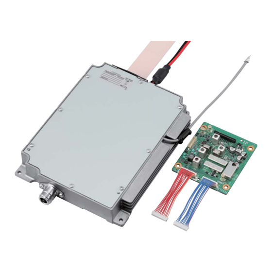
Related Manuals for Icom UX-9100


Summary of Contents for Icom UX-9100
- Page 1 1200 MHz BAND UNIT S-14804XZ-C1 Sep. 2011...
- Page 2 8. READ the instructions of the test equipment throughly before connecting it to the unit. Icom, Icom Inc. and the Icom logo are registered trademarks of Icom Incorporated (Japan) in Japan, the United States, the United Kingdom, Germany, France, Spain, Russia and/or other countries.
-
Page 3: Table Of Contents
TABLE OF CONTENTS SECTION SPECIFICATIONS SECTION INSIDE VIEWS SECTION CIRCUIT DESCRIPITON RECEIVER CIRCUITS............3-1 TRANSMITTER CIRCUITS . - Page 4 SECTION 1. SPECIFICATIONS • Frequency coverage [KOR] 1260–1300 MHz (With IC-9100) [USA], [CHN], [EXP] 1240–1320 MHz* 1240–1300 MHz [EUR], [EUR-01] 1240–1300 MHz [ESP], [FRA] [ITR] 1240–1300 MHz 1270–1298 MHz [TPE] 1260–1265 MHz 50 Ω (Nominal) • Antenna impedance • Operating temperature range ±0˚C to +50˚C (32˚F to +122˚F) •...
- Page 5 SECTION 2. INSIDE VIEWS • MAIN-B UNIT PWR AMP (IC21) APC AMP (IC31) (Q282) RF AMP (Q281) YGR AMP (IC141) Lo AMP (IC181) R9V REGURATER IF AMP (Q170) (IC111) (IC931) 1st IF CIRCUIT +5 REGURATER (IC162) REG CTRL (Q167) REG CTRL 2nd MIXER (Q165) PLL IC...
- Page 6 • RF-C UNIT S/P CONVERTER (IC81) TIPLEXER (IC52) TIPLEXER (IC55) IF AMP (Q501) TIPLEXER (IC54) LTIPLEXER (IC53) 3rd MIXER IF AMP (D151) (Q251) BUFF IF AMP (IC121) (Q201) 3rd MIXER IF AMP (D152) (Q202) LO AMP (Q121) T8V REGURATOR (Q34) BUFF T8V REGURATOR (Q321)
-
Page 7: Circuit Descripiton
SECTION 3. CIRCUIT DESCRIPTION 3RD RX IF CIRCUITS (RF-C UNIT) 3-1 RECEIVER CIRCUITS The 2nd RX IF signal from the 2nd RX IF circuits is divided RF CIRCUITS (MAIN-B UNIT) into two paths, and then each signal is passed through the The RX signal from the antenna is passed through the TX LPF (L201, C201, C203/L202, C202, C204) and applied to power detector (D502, D503), and TX/RX line SW (RL51) -
Page 8: Transmitter Circuits
3-2 TRANSMITTER CIRCUITS 2ND TX IF CIRCUITS (RF-C and MAIN-B UNITs) TX AMP CIRCUITS (MAIN-B UNIT) The 10.95 MHz 2nd TX IF signal from the MAIN-B UNIT The TX signal from the 1st TX IF circuits is applied to the of IC-9100 is passed through the BPF (L401–L403, C401, YGR AMP (IC141). -
Page 9: Frequency Synthesizer Circuits
The 30.2 MHz reference frequency signal from the MAIN-B C630, C633–C638), amplified by the AMP (IC601), passed UNIT of IC-9100 is applied to the MAIN-B UNIT of UX-9100, through the LPF (L621, C644–C646), and then applied to through J312. The reference signal is used as the reference the doubler (D601, L606), resulting in the 498.05–538.05... -
Page 10: Voltage Diagrams
3-4 VOLTAGE DIAGRAMS Voltage from the power supply is routed throughout the unit, via regulators and switches. -12V Q171 D168 CTRL MAIN-B UNIT +14V Q166 Q168 D166 1TX9 +14V Q167 CTRL Q170 RF-C UNIT 1RX9 D167 CTRL Q172 D169 CTRL IC161 IC162 3 - 4... -
Page 11: Adjustment Procedures
Capacity : More than 2 W ¤ GENERAL CONNECTION STANDARD SIGNAL GENERATOR (1–1500 MHz) RF POWER METER (20 W/50 Ω) RF-C UNIT (UX-9100) MAIN-B UNIT [1200MHz ANT] (UX-9100) [EXT SP (MAIN)] DO NOT transmit while an SSG is connected to AC MILLIVOLT METER the antenna connector. - Page 12 4-2 RECEIVE ADJUSTMENTS TRANSCEIVER’S ADJUSTMENT ADJUSTMENT OPERATION VALUE CONDITION ITEM PEAK • Frequency : 1270.000 MHz 1) Disconnect the "MDRIF" line from the Maximum L203 (MAIN band) pins 6 and 7 of J3 (RF-C UNIT). level. (RF-C UNIT) • Mode : SSB 2) Connect a spectrum analyzer to the "MDRIF"...
-
Page 13: Receive Adjustment
4-2 RECEIVE ADJUSTMENTS (Continued) TRANSCEIVER’S ADJUSTMENT ADJUSTMENT OPERATION VALUE CONDITION ITEM IMAGE • Frequency : 1270.000 MHz 1) Disconnect the spectrum analyzer from Minimum AF (MAIN band) the pins 6 and 7 ("MDRIF" line) of J3 (RF-C output level. • Mode : SSB UNIT). - Page 14 4-3 TRANSMIT ADJUSTMENTS TRANSCEIVER’S ADJUSTMENT ADJUSTMENT OPERATION VALUE CONDITION ITEM Max. CW TX PEAK AND 1 • Frequency : 1300.000 MHz • S e t t h e t r i m m e r r e g i s t e r s a n d R61, R83 RESIDUAL AM (MAIN band)
-
Page 15: Transmit Adjustment
4-3 TRANSMIT ADJUSTMENTS (Continued) TRANSCEIVER’S ADJUSTMENT ADJUSTMENT OPERATION VALUE CONDITION ITEM TX TOTAL GAIN • Frequency : 1270.000 MHz • Set the SSG as; † (MAIN band) Level : 75 dBµ (–32 dBm) • Mode : RTTY • Connect an RF power meter to (MAIN-B UNIT) •... - Page 16 SECTION 5. PARTS LIST [RF-C UNIT] [RF-C UNIT] PARTS PARTS DESCRIPTION DESCRIPTION LOCATION LOCATION IC51 1180003580 S.REG NJM79L05UA-TE1-#ZZZB 9.1/16.7 7030010570 S.RES ERJ1TYJ 4R7U (4.7) 64.7/16.0 IC52 1130013110 S.IC KIC7W53FK-RTK/P 24.6/60.7 7030003500 S.RES ERJ3GEYJ 332 V (3.3K) 58.7/8.9 IC53 1130013110 S.IC KIC7W53FK-RTK/P 28.4/54.9 7030003500 S.RES ERJ3GEYJ 332 V (3.3K)
- Page 17 [RF-C UNIT] [RF-C UNIT] PARTS PARTS DESCRIPTION DESCRIPTION LOCATION LOCATION R511 7030003320 S.RES ERJ3GEYJ 101 V (100) 48.0/71.4 C326 4030007010 S.CER C1608 CH 1H 100D-T 33.7/19.3 R512 7030003290 S.RES ERJ3GEYJ 560 V (56) 58.9/65.6 C328 4550003220 S.TAN TEESVA 1E 105M8R 37.5/21.3 R601 7030003200 S.RES ERJ3GEYJ 100 V (10)
- Page 18 [MAIN-B UNIT] [MAIN-B UNIT] PARTS PARTS DESCRIPTION DESCRIPTION LOCATION LOCATION IC21 1150002191 IC RA18H1213G1-121 FI241 2040001650 S.SAW WF447B-T 71.8/8.7 IC31 1110001220 S.IC BA4558F E2 141.4/17.5 FI271 2040001660 S.FIL LFB431G28SN1A362 IC111 1110006870 S.IC UPC2709TB-E3 73.3/21.5 (LFSN30N18C1) 109.2/9.9 IC131 1110007740 S.IC UPC8187TB-E3-A 98.8/21.4 FI281 2040001660 S.FIL...
- Page 19 [MAIN-B UNIT] [MAIN-B UNIT] PARTS PARTS DESCRIPTION DESCRIPTION LOCATION LOCATION L622 6200005671 S.COI ELJRE 12NGFA 50.8/52.1 7030003500 S.RES ERJ3GEYJ 332 V (3.3K) 153.9/23.6 L623 6200005741 S.COI ELJRE 47NGFA 44.0/84.4 7030003540 S.RES ERJ3GEYJ 682 V (6.8K) 161.2/34.2 L624 6200011650 S.COI LQW18AN68NG00D 52.3/82.6 7030003500 S.RES ERJ3GEYJ 332 V (3.3K) 158.8/33.4...
- Page 20 [MAIN-B UNIT] [MAIN-B UNIT] PARTS PARTS DESCRIPTION DESCRIPTION LOCATION LOCATION R504 7030004030 S.RES ERJ3GEYJ 5R6 V (5.6) 55.6/67.0 4030011770 S.CER C1608 CH 1H 060B-T 22.9/9.9 R505 7030003430 S.RES ERJ3GEYJ 821 V (820) 54.8/65.0 4030007090 S.CER C1608 CH 1H 470J-T 104.3/49.3 R510 7030003440 S.RES ERJ3GEYJ 102 V (1K) 39.8/68.0...
- Page 21 [MAIN-B UNIT] [MAIN-B UNIT] PARTS PARTS DESCRIPTION DESCRIPTION LOCATION LOCATION C148 4030006880 S.CER C1608 JB 1H 472K-T 103.3/34.1 C286 4030011600 S.CER C1608 JB 1E 104K-T 134.3/24.5 C149 4030006860 S.CER C1608 JB 1H 102K-T 104.3/32.7 C287 4030006880 S.CER C1608 JB 1H 472K-T 134.3/23.2 C150 4030007010 S.CER C1608 CH 1H 100D-T...
- Page 22 [MAIN-B UNIT] [MAIN-B UNIT] PARTS PARTS DESCRIPTION DESCRIPTION LOCATION LOCATION C611 4030006860 S.CER C1608 JB 1H 102K-T 48.4/54.7 C733 4030006860 S.CER C1608 JB 1H 102K-T 25.5/54.7 C612 4030007130 S.CER C1608 CH 1H 101J-T 48.6/56.3 C734 4030007060 S.CER C1608 CH 1H 270J-T 29.9/52.0 C613 4030006860 S.CER C1608 JB 1H 102K-T...
- Page 23 [MAIN-B UNIT] PARTS DESCRIPTION LOCATION 7030012280 JUM RD25T0R0 7030012280 JUM RD25T0R0 W243 9024801019 JUM 74/98/020/X98/X98 W290 7030012290 JUM RDS2T0R0 EP10 6910000970 BEA DL-2OP 2.6-3-1.2H EP12 6910000970 BEA DL-2OP 2.6-3-1.2H EP25 6910020400 SHE FERRITE SHEET(AA) (40X15X0.5) EP301 6910015970 S.BEA MMZ1608B 301CT-AS 57.0/53.7 EP331 6910014640 S.BEA...
- Page 24 SECTION 6. MECHANICAL PARTS [CHASSIS PARTS] [MAIN-B UNIT] ORDER ORDER DESCRIPTION QTY. DESCRIPTION QTY. W313* 8970025100 0.8DCOAXIAL100MM B09A/B09A J26* 6910001040 IPS-1136 W331 8900017630 OPC-1876 J311* 6510026610 26FMN-BTK-A (LF) (SN) W1001 8600037280 EX2356 P1001*P1002CH2 J313* 6510014961 B2B-ZR-SM4-TF (LF) (SN) W2001 8600037290 EX2356 P2001*P2002CH2 W3001 8600037300 EX2356 P3001*P3002CH2 8970025090 1.5D 250MM (#2356 MA-B W3)
- Page 25 MP5(C)×2 MP101(C)×2 J1(C) MP3(C) MP102(C) MP1(C) MP15(C) MP17(C) MP11(C) MP331(C) MP18(C) MP12(C) MAIN-B UNIT W3001(C) EP25(M) RF-C UNIT J601 W331(C) IC21(M) W1001(C) MP8(C)×14 W2001(C) MP22(C) MP9(C)×2 MP16(C) MP26(C) MP14(C) MP103(C) MP2(C) MP7(C)×8 UNIT ABBREVIATIONS (C): CHASSIS PARTS (M): MAIN-B UNIT 6 - 2...
- Page 26 SECTION 7. BOARD LAYOUTS The combination of this page and next page shows the top side and bottom side of actual P.C. board. • MAIN-B UNIT (TOP VIEW) Q173 CHASSIS MP1 D168 C173 C165 C172 IC161 Q166 C167 C302 R168 D167 R301 L311...
- Page 27 The combination of this page and next page shows the top side and bottom side of actual P.C. board. • MAIN-B UNIT (BOTTOM VIEW) C344 D171 R171 EP351 R172 R518 L626 R521 L751 EP602 C912 C502 C755 L911 L913 C752 R520 MP33 C916...
- Page 28 The combination of top side and bottom side of this • RF-C UNIT (TOP VIEW) C306 C401 C402 PDAT5 C305 PCK5 L401 122ST5 IC56 12DST C307 R354 12DSTU R622 Q604 12IUP3 OPB1 C404 C308 DRESL5 R360 R621 Q603 L403 R315 1R2RXS IC52 C405...
- Page 29 The combination of top side and bottom side of this • RF-C UNIT (BOTTOM VIEW) C303 C302 R309 R305 R351 R353 C304 C351 R312 C352 IC351 IC301 R303 R301 C353 R357 R304 R300 R355 C301 R253 C206 C207 R603 R364 R257 R204 R321...
- Page 30 SECTION 8. BLOCK DIAGRAM 1FOR IC31 BA4558 RF-C MAIN-B FI141 LFSN30N18C1280B Q501 IC111 FI101 IC131 IC141 10.95MHz 3SK264 2nd IF 2SC2712 HSB88WS UPC2709 WF447B UPC8187TB UPC1678G LFSN30N18C1280B from IC-9100 MAIN 10.95MHz 1R2TIF DRIVE 1st IF IC21 243.95MHz 2SK2854 RA18H1213G1 D502:HSU88 D503:HSU88 12PR IC181...
- Page 31 SECTION 9. VOLTAGE DIAGRAM • MAIN-B UNIT (1/3) RXIF TXIF 1TX9 IC161 IC162 R171 BA09T TA7805F NLV25T R172 12PV 12PV 12PR 12PR 1FOR 1FOR 12TP 12TP 12AT 12AT MAIN-B(2) C106 HSB88WS-E #617DB-1919=P3 #617DB-1919=P3 KDS114 0.0047 NLV25T NLV25T 2SC2712 1RX9 150P EVM3VBQ2 Q163 1TX9...
- Page 32 • MAIN-B UNIT (2/3) RD25T0R0 ELJRE CP401 D503 HSU88-E C326 EP10 R805 ERJ3GE-JPW 2SK2854 470P EP12 ELJRE R351 EP351 D504 1SS385 R863 ERJ3GE-JPW RD25T0R0 ELJRE IC31 BA4558F 2SD1801 470K LQN21A DAN222 LFSN30N18C1280B 0.001 DTC144EU R145 2SC2712 2SC2712 ELJRE 1TX9 R130 CP31 IC131 FI141...
- Page 33 • MAIN-B UNIT (3/3) Q502 R521 DTC144EU ERJ3GE-JPW 249.0125-264.0125MHz EP608 IC501 L624 UPD120N33TA CASE-BM7H-LF IC602 L620 L618 124.50625 - 132.00625 MHz C616 L617 L616 4 GND LQW18AN68NG00D UPC2709TB LQW18AN68NG00D ELJRE 0.0047 ELJRE LQW18AN22NG00 C630 C626 C622 L623 3 GND 5 NC OUT 5 EP501 2 GND...
- Page 34 R608 1R2REF(30.2MHz) ERJ3GE-JPW 12DSTU 12IUP3 PDAT PDAT R609 12DST 12DT3 12PREL RCSTB 12ST 122ST5 2LST_ 12MST R615 TO IC-9100 PLL TO UX-9100 MAIN-B R610 R616 12PV 12DT3 12DT 6.8K PCK5 2LST_ R611 R612 2LST ERJ3GE-JPW PDAT5 PDAT IC361 IC361 OPB1_...
- Page 35 Highway 17 Delta, B.C., V4K 5B8, Canada : http://www.icomspain.com Phone : +1 (604) 952-4266 Fax : +1 (604) 952-0090 E-mail : icom@icomspain.com : http://www.icomcanada.com E-mail : info@icomcanada.com Blacksole House, The Boulevard, Altira Business Park, Herne Bay, CT6 6GZ, UK Phone : +44 (01227) 741741...
- Page 36 S-14804XZ-C1 1-1-32, Kamiminami, Hirano-ku, Osaka 547-0003, Japan © 2011 Icom Inc.
Need help?
Do you have a question about the UX-9100 and is the answer not in the manual?
Questions and answers