Table of Contents
Advertisement
Quick Links
DYNAMIC ENGINEERING
150 DuBois, Suite C Santa Cruz, CA 95060
(831) 457-8891, Fax: (831) 457-4793
www.dyneng.com
sales@dyneng.com
Est. 1988
User Manual
PMC-BiSerial-III SDLC
8 channel
SDLC Interface
PMC Module
Revision A1
Corresponding Hardware: Revision E
10-2005-0205
Corresponding Firmware: Revision B
Advertisement
Table of Contents

Related Manuals for Dynamic Engineering PMC-BiSerial-III SDLC

Summary of Contents for Dynamic Engineering PMC-BiSerial-III SDLC
- Page 1 DYNAMIC ENGINEERING 150 DuBois, Suite C Santa Cruz, CA 95060 (831) 457-8891, Fax: (831) 457-4793 www.dyneng.com sales@dyneng.com Est. 1988 User Manual PMC-BiSerial-III SDLC 8 channel SDLC Interface PMC Module Revision A1 Corresponding Hardware: Revision E 10-2005-0205 Corresponding Firmware: Revision B...
- Page 2 Dynamic Engineering has made every effort to ensure that this manual is accurate and complete. Still, the company reserves the right...
-
Page 3: Table Of Contents
Table of Contents PRODUCT DESCRIPTION THEORY OF OPERATION ADDRESS MAP PROGRAMMING REGISTER DEFINITIONS BIS3_BASE BIS3_ID BIS3_IO_DATA BIS3_IO_DIR BIS3_IO_TERM BIS3_IO_MUX BIS3_IO_UCNTL BIS3_IO_RDBK BIS3_IO_RDBKUPR BIS3_SWITCH BIS3_PLL_CMD, PLL_RDBK BIS3_SDLC_CNTL7-0 BIS3_INT_STAT BIS3_I2OAR Mode Resource Mapping Channel I/O Line Mapping Interrupts Loop-back PMC PCI PN1 INTERFACE PIN ASSIGNMENT PMC PCI PN2 INTERFACE PIN ASSIGNMENT BISERIAL III FRONT PANEL I/O PIN ASSIGNMENT APPLICATIONS GUIDE... - Page 4 Interfacing CONSTRUCTION AND RELIABILITY THERMAL CONSIDERATIONS WARRANTY AND REPAIR SERVICE POLICY OUT OF WARRANTY REPAIRS FOR SERVICE CONTACT: SPECIFICATIONS ORDER INFORMATION SCHEMATICS Embedded Solutions Page 4 of 37...
- Page 5 List of Figures FIGURE 1 PMC BISERIAL-III BASE BLOCK DIAGRAM FIGURE 2 PMC BISERIAL-III SDLC BLOCK DIAGRAM FIGURE 3 PMC BISERIAL-III SDLC INTERNAL ADDRESS MAP FIGURE 4 PMC BISERIAL-III SDLC BASE CONTROL REGISTER BIT MAP FIGURE 5 PMC BISERIAL-III SDLC DESIGN ID REGISTER BIT MAP FIGURE 6 PMC BISERIAL-III SDLC PARALLEL OUTPUT DATA BIT MAP FIGURE 7...
-
Page 6: Product Description
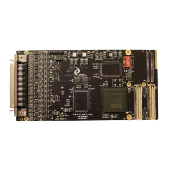
Product Description The PMC BiSerial-III-SDLC is part of the PMC Module family of modular I/O components by Dynamic Engineering. The PMC BiSerial-III is capable of providing multiple serial protocols. The SDLC protocol implemented provides 8 full-duplex SDLC I/O channels. Other custom interfaces are available. We will redesign the state machines and create a custom interface protocol. - Page 7 PMC Carrier board, with final system implementation uses a different one. Contact Dynamic Engineering for a copy of this specification. It is assumed that the reader is at least casually familiar with this document and basic logic design.
- Page 8 All configuration registers support read and write operations for maximum software convenience, and all addresses are long word aligned. Interrupts are supported by the PMC BiSerial-III-SDLC. An interrupt can be configured to occur at the end of each transmitted message-frame, at the end of all message- frames transmitted, at the end of a received message-frame or when an abort character has been received.
-
Page 9: Theory Of Operation
Theory of Operation The PMC BiSerial-III-SDLC features a Xilinx FPGA. The FPGA contains all of the registers and protocol controlling elements of the BiSerial III design. Only the PLL, transceivers, and switches are external to the Xilinx device. The PCI interface to the host CPU is controlled by a logic block within the Xilinx. The BiSerial III design requires one wait state for read or write cycles to any address. - Page 10 If the TX clear is enabled, the transmitter will be automatically disabled and the TX interrupt will be asserted when no more message frames have been requested. If the TX clear is not enabled, the transmitter will remain enabled after the last message, but the TX interrupt will still be asserted.
- Page 11 The PLL is configured to supply a 48 MHz signal on its clock A output. This is used to sample the transmit reference clock to detect transitions. These transitions are used to determine when to drive the next data bit onto the transmit data I/O line. The transmitter clock reference can be supplied by an external source or an internal clock reference provided by PLL clock B.
-
Page 12: Address Map
Address Map BIS3_BASE 0x0000 Base control register BIS3_ID 0x0004 ID register BIS3_IO_DATA 0x0010 Data register 31 - 0 BIS3_IO_DIR 0x0014 Direction register 31 - 0 BIS3_IO_TERM 0x0018 Termination register 31 - 0 BIS3_IO_MUX 0x001C Mux register 31 - 0 BIS3_IO_UCNTL 0x0020 Upper control register 33, 32 BIS3_SWITCH... -
Page 13: Programming
Programming Programming the PMC BiSerial-III-SDLC requires only the ability to read and write data from the host. The base address of the module refers to the first user address for the slot in which the PMC is installed. This address is determined during system configuration of the PCI bus. -
Page 14: Register Definitions
Register Definitions BIS3_BASE [$00] BiSerial III Base Control Register Port read/write Base Control Register DATA BIT DESCRIPTION 31-4 Spare I2O CLR I2O EN Interrupt Set Interrupt Enable Master FIGURE 4 PMC BISERIAL-III SDLC BASE CONTROL REGISTER BIT MAP All bits are active high and are reset on power-up or reset command. Interrupt Enable Master: When '1' allows interrupts generated by the PMC-BiSerial-III-SDLC to be driven onto the carrier (INTA). -
Page 15: Bis3_Id
BIS3_ID [$04] BiSerial III FLASH status/Driver Status Port read only Design Number / FLASH Revision DATA BIT DESCRIPTION 31-16 Design/Driver ID 15-0 FLASH revision FIGURE 5 PMC BISERIAL-III SDLC DESIGN ID REGISTER BIT MAP The Design/Driver ID for the SDLC project is 0x0003. The FLASH revision is currently 0x0001, but will be updated as features are added or revisions made. -
Page 16: Bis3_Io_Dir
BIS3_IO_DIR [$14] BiSerial III Direction Port read/write Direction Control Port DATA BIT DESCRIPTION 31-0 Parallel Port Direction Control bits FIGURE 7 PMC BISERIAL-III SDLC DIRECTION CONTROL PORT When set (‘1’) the corresponding bit in the parallel port is a transmitter. When cleared (‘0’) the corresponding bit is a receiver. -
Page 17: Bis3_Io_Ucntl
BIS3_IO_MUX [$1C] BiSerial III Mux Port read/write Multiplexor Control Port DATA BIT DESCRIPTION 31-0 Parallel Port Mux Control bits FIGURE 9 PMC BISERIAL-III SDLC MUX CONTROL PORT When set (‘1’) the corresponding bit is set to State-Machine control. When cleared (‘0’) the corresponding bit is set to parallel port operation. -
Page 18: Bis3_Io_Rdbk
BIS3_IO_RDBK [$C0] BiSerial III I/O Read-Back Port read only I/O Read-Back Port DATA BIT DESCRIPTION 31-0 I/O Data 31-0 FIGURE 11 PMC BISERIAL-III SDLC I/O READBACK PORT The I/O lines can be read at any time. The value is not filtered in any way. If the transceivers are set to TX by the parallel port or state-machine then the read-back value will be the transmitted value. -
Page 19: Bis3_Switch
BIS3_SWITCH [$24] BiSerial III Switch Port read only User Switch Port DATA BIT DESCRIPTION 31-24 Spare 23-16 sw7-0 15-0 Spare FIGURE 13 PMC BISERIAL-III SDLC SWITCH PORT The Switch Read Port has the user bits. The user bits are connected to the eight dip- switch positions. -
Page 20: Bis3_Pll_Cmd, Pll_Rdbk
Cypress® CyberClocks utility, and then programming the resulting control words into the PLL using this PLL Control port. The interface can be further simplified by using the Dynamic Engineering driver to take care of the low-level bit manipulation requirements. -
Page 21: Bis3_Sdlc_Cntl7-0
BIS3_SDLC_CNTL7-0 [$B0, A0, 90, 80, 70, 60, 50, 40] BiSerial III SDLC Control Registers SDLC Control Registers DATA BIT DESCRIPTION Idle Detected/Clear (see note after description) Abort Detected/Clear (see note after description) 29-25 spare SDLC Internal Clock Select Send an Abort (write only) Load Transmit End Address (write only) Load Transmit Start Address/SDLC Done Load Receive Start Address/SDLC Sending Data... - Page 22 Transmit Interrupt Enable: When this bit is a one the transmitter interrupt is enabled. The interrupt will occur at when the transmit state-machine reaches the end address stored in the transmitter end-address register and there is not another message pending. When this bit is a zero the interrupt status will still be latched, but will not cause an interrupt to occur.
- Page 23 Load Receive Start Address/SDLC Sending Data: When this bit is a one the value in the address input field is loaded into the receiver start-address register. When this bit is a zero no action is taken. When this bit is read as a one, the transmitter is actively sending data.
-
Page 24: Bis3_Int_Stat
BIS3_INT_STAT [$CC] BiSerial III Interrupt Status and Clear Register Interrupt Status and Clear Register DATA BIT DESCRIPTION 31-0 Channel Interrupt or Clear bit FIGURE 16 PMC BISERIAL-III SDLC INTERRUPT STATUS REGISTER Each bit is set when an interrupt occurs on the associated channel. Each bit can be cleared by writing to the register with the same bit position set (‘1’). -
Page 25: Mode Resource Mapping
Resource Mapping I/O Mapping for SDLC Channels Interrupt Mapping for SDLC Channels I/O line SDLC Function Int line SDLC Function I/O 0 Transmit Data 0 Int 0 Transmit Interrupt I/O 1 Receive Data 0 Int 1 TX Frame Done I/O 2 Transmit Clock 0 Int 2 Receive Interrupt... -
Page 26: Channel I/O Line Mapping
Channel I/O Line Mapping SDLC channel 0: pin 35 – SDLC transmit data => I/O 0: pin 1 +, pin 36 – SDLC receive data => I/O 1: pin 2 +, pin 37 – SDLC transmit clock=> I/O 2: pin 3 +, pin 38 –... -
Page 27: Interrupts
Interrupts PMC BiSerial-III interrupts are treated as auto-vectored. When the software enters into an exception handler to deal with a PMC BiSerial-III interrupt the software must read the status register to determine the cause(s) of the interrupt, clear the interrupt request(s) and process accordingly. -
Page 28: Loop-Back
Loop-back The Engineering kit has reference software, which includes an external loop-back test. The SDLC version of the PMC-BiSerial-III utilizes a 68 pin SCSI II front panel connector. The test requires an external cable with the following pins connected. Using our HDEterm68 test fixture make the following connections (TP2 unless noted). Note: TP1, 2 are both ordered as follows: 1, 35, 2, 36, 3, 37…32, 66, 33, 67, 34, 68. - Page 29 Four short wires per header are added to the bottom of the HDEterm68. Channel 0: TP1 2 to 36, TP1 38 to 4, TP1 3 to TP2 3 and TP1 37 to TP2 37 Channel 1: TP1 6 to 40, TP1 42 to 8, TP1 7 to TP2 7 and TP1 41 to TP2 41 Channel 2: TP1 10 to 44, TP1 46 to 12, TP1 11 to TP2 11 and TP1 45 to TP2 45 Channel 3: TP1 14 to 48, TP1 50 to 16, TP1 15 to TP2 15 and TP1 49 to TP2 49 Channel 4: TP1 18 to 52, TP1 54 to 20, TP1 19 to TP2 19 and TP1 53 to TP2 53...
-
Page 30: Pmc Pci Pn1 Interface Pin Assignment
PMC PCI Pn1 Interface Pin Assignment The figure below gives the pin assignments for the PMC Module PCI Pn1 Interface on the PMC BiSerial-III. See the User Manual for your carrier board for more information. Unused pins may be assigned by the specification and not needed by this design. -12V(unused) INTA# BUSMODE1#... -
Page 31: Pmc Pci Pn2 Interface Pin Assignment
PMC PCI Pn2 Interface Pin Assignment The figure below gives the pin assignments for the PMC Module PCI Pn2 Interface on the PMC BiSerial-III. See the User Manual for your carrier board for more information. Unused pins may be assigned by the specification and not needed by this design. +12V(unused) RST# BUSMODE3#... -
Page 32: Biserial Iii Front Panel I/O Pin Assignment
The figure below gives the pin assignments for the PMC Module I/O Interface on the PMC BiSerial-III. Also, see the User Manual for your carrier board for more information. For customized version, or other options, contact Dynamic Engineering. IO_0p IO_0m... -
Page 33: Applications Guide
Applications Guide Interfacing The pin-out tables are displayed with the pins in the same relative order as the actual connectors. The pin definitions are defined with noise immunity in mind. The pairs are chosen to match standard SCSI II/III cable pairing to allow a low cost commercial cable to be used for the interface. - Page 34 PMC Modules are conceived and engineered for rugged industrial environments. The PMC BiSerial-III is constructed out of 0.062 inch thick High Temp FR4 material. The PC Boards are ROHS compliant. Dynamic Engineering has selected gold immersion processing to provide superior performance, and reliability (not subject to tin whisker issues).
- Page 35 For service on Dynamic Engineering Products not purchased directly from Dynamic Engineering, contact your reseller. Products returned to Dynamic Engineering for repair by other than the original customer will be treated as out-of-warranty.
- Page 36 Specifications Host Interface: (PMC) PCI Mezzanine Card - 32 bit, 33 MHz Serial Interface: 8 Full Duplex SDLC serial interfaces. 16-bit word size, LSB first. TX Data rates generated: 40 MHz oscillator used to generate 48 MHz I/O clock sampling frequency, 3 MHz Internal transmit clock.
- Page 37 “Corresponding Hardware Revision. ” This information is not necessarily current or complete manufacturing data, nor is it part of the product specification. All information provided is Copyright Dynamic Engineering Embedded Solutions Page 37 of 37...
Need help?
Do you have a question about the PMC-BiSerial-III SDLC and is the answer not in the manual?
Questions and answers