Table of Contents
Advertisement
Advertisement
Table of Contents
Troubleshooting

Related Manuals for Panasonic KX-TG6511BXB


Summary of Contents for Panasonic KX-TG6511BXB
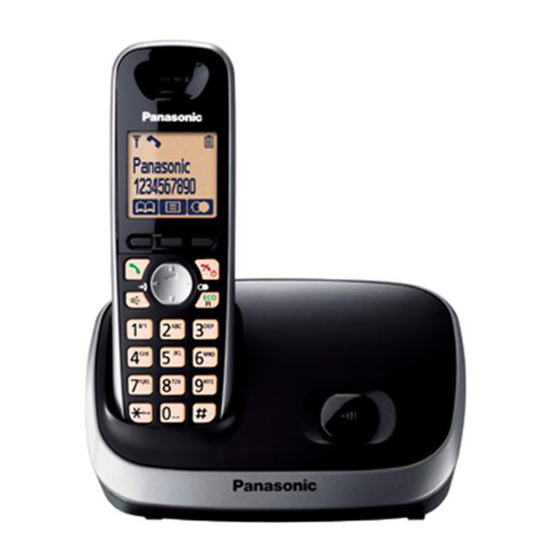
- Page 1 ORDER NO. KM41009246CE Telephone Equipment KX-TG6511BXB Model No. KX-TG6512BXB KX-TG6513BXB KX-TG6519BXB KX- TGA651BXB Digital Cordless Phone B: Black Version (for Middle Near East and Africa) © Panasonic System Networks Co., Ltd. 2010 Unauthorized copying and distribution is a violation of law.
- Page 2 KX-TG6511BXB/KX-TG6512BXB/KX-TG6513BXB/KX-TG6519BXB/KX-TGA651BXB...
-
Page 3: Table Of Contents
KX-TG6511BXB/KX-TG6512BXB/KX-TG6513BXB/KX-TG6519BXB/KX-TGA651BXB TABLE OF CONTENTS PAGE PAGE 1 Safety Precautions----------------------------------------------- 4 15.2. Cabinet and Electrical Parts (Handset)------------- 75 1.1. For Service Technicians --------------------------------- 4 15.3. Cabinet and Electrical Parts (Charger Unit) ------- 76 2 Warning -------------------------------------------------------------- 4 15.4. Accessories------------------------------------------------ 77 2.1. Battery Caution--------------------------------------------- 4 15.5. -
Page 4: Safety Precautions
KX-TG6511BXB/KX-TG6512BXB/KX-TG6513BXB/KX-TG6519BXB/KX-TGA651BXB 1 Safety Precautions 1.1. For Service Technicians • Repair service shall be provided in accordance with repair technology information such as service manual so as to prevent fires, injury or electric shock, which can be caused by improper repair work. -
Page 5: Discarding Of P.c. Board
KX-TG6511BXB/KX-TG6512BXB/KX-TG6513BXB/KX-TG6519BXB/KX-TGA651BXB 2.2.1. Suggested PbF Solder There are several types of PbF solder available commercially. While this product is manufactured using Tin, Silver, and Copper (Sn+Ag+Cu), you can also use Tin and Copper (Sn+Cu) or Tin, Zinc, and Bismuth (Sn+Zn+Bi). Please check the manufacturer’s specific instructions for the melting points of their products and any precautions for using their product with other materials. -
Page 6: Specifications
KX-TG6511BXB/KX-TG6512BXB/KX-TG6513BXB/KX-TG6519BXB/KX-TGA651BXB 3 Specifications Note: • Design and specifications are subject to change without notice. Note for Service: • Operation range: Up to 300 m outdoors, Up to 50 m indoors, depending on the condition. • Analog telephone connection: Telephone Line... -
Page 7: Technical Descriptions
KX-TG6511BXB/KX-TG6512BXB/KX-TG6513BXB/KX-TG6519BXB/KX-TGA651BXB 4 Technical Descriptions 4.1. Block Diagram (Base Unit) -
Page 8: Circuit Operation (Base Unit)
KX-TG6511BXB/KX-TG6512BXB/KX-TG6513BXB/KX-TG6519BXB/KX-TGA651BXB 4.2. Circuit Operation (Base Unit) 4.2.1. Outline Base Unit consists of the following ICs as shown in Block Diagram (Base Unit) (P.7). • DECT BBIC (Base Band IC): IC7 - Handling all the audio, signal and data processing needed in a DECT base unit... - Page 9 KX-TG6511BXB/KX-TG6512BXB/KX-TG6513BXB/KX-TG6519BXB/KX-TGA651BXB 4.2.2. Power Supply Circuit The power is supplied to the DECT BBIC, RF Module, EEPROM and Charge Contact from AC Adaptor (+6.5 V) as shown in Fig.101. The power supply is as follows; • DECT BBIC (IC7): DC Jack (+6.5 V) → IC2 → IC7 DC Jack (+6.5 V) →...
- Page 10 KX-TG6511BXB/KX-TG6512BXB/KX-TG6513BXB/KX-TG6519BXB/KX-TGA651BXB 4.2.3. Telephone Line Interface <Function> • Bell signal detection • Clip signal detection • ON/OFF hook circuit Bell & Clip (: Calling Line Identification Presentation: Caller ID) signal detection: In the standby mode, Q3 is open to cut the DC loop current and decrease the ring load.
-
Page 11: Block Diagram (Handset)
KX-TG6511BXB/KX-TG6512BXB/KX-TG6513BXB/KX-TG6519BXB/KX-TGA651BXB 4.3. Block Diagram (Handset) -
Page 12: Circuit Operation (Handset)
KX-TG6511BXB/KX-TG6512BXB/KX-TG6513BXB/KX-TG6519BXB/KX-TGA651BXB 4.4. Circuit Operation (Handset) 4.4.1. Outline Handset consists of the following ICs as shown in Block Diagram (Handset) (P.11). • DECT BBIC (Base Band IC): IC1 - All data signals (forming/analyzing ACK or CMD signal) - All interfaces (ex: Key, Detector Circuit, Charge, DC/DC Converter, EEPROM, LCD, RF Power Amp.) -
Page 13: Circuit Operation (Charger Unit)
KX-TG6511BXB/KX-TG6512BXB/KX-TG6513BXB/KX-TG6519BXB/KX-TGA651BXB 4.5. Circuit Operation (Charger Unit) 4.5.1. Power Supply Circuit The power supply is as shown. -
Page 14: Signal Route
KX-TG6511BXB/KX-TG6512BXB/KX-TG6513BXB/KX-TG6519BXB/KX-TGA651BXB 4.6. Signal Route... -
Page 15: Location Of Controls And Components
KX-TG6511BXB/KX-TG6512BXB/KX-TG6513BXB/KX-TG6519BXB/KX-TGA651BXB 5 Location of Controls and Components Refer to the Operating Instructions. Note: You can download and refer to the Operating Instructions (Instruction book) on TSN Server. 6 Installation Instructions Refer to the Operating Instructions. Note: You can download and refer to the Operating Instructions (Instruction book) on TSN Server. -
Page 16: Service Mode
KX-TG6511BXB/KX-TG6512BXB/KX-TG6513BXB/KX-TG6519BXB/KX-TGA651BXB 8 Service Mode 8.1. Engineering Mode 8.1.1. Base Unit... - Page 17 KX-TG6511BXB/KX-TG6512BXB/KX-TG6513BXB/KX-TG6519BXB/KX-TGA651BXB Frequently Used Items (Base Unit) ex.) Items Address Default Data New Data Remarks C-ID (FSK) sensitivity 04 8B 01 (6 dB up) 02 (12 dB up) When hex changes from “00” to “01” or “02”, gain increases by 6 dB or 12 dB.
- Page 18 KX-TG6511BXB/KX-TG6512BXB/KX-TG6513BXB/KX-TG6519BXB/KX-TGA651BXB 8.1.2. Handset...
- Page 19 KX-TG6511BXB/KX-TG6512BXB/KX-TG6513BXB/KX-TG6519BXB/KX-TGA651BXB Frequently Used Items (Handset) ex.) Items Address Default Data New Data Possible Adjusted Possible Adjusted Remarks Value MAX (hex) Value MIN (hex) Sending level 03 17 Adjusted value Given value (*2) Receiving level 03 18 Adjusted value Given value...
-
Page 20: Copying Phonebook Items When Repairing
KX-TG6511BXB/KX-TG6512BXB/KX-TG6513BXB/KX-TG6519BXB/KX-TGA651BXB 8.2. Copying Phonebook Items when Repairing You can copy the handset phonebook to another (compatible Panasonic) handset. This will help to save the original phonebook data which the customer has registered. Refer to the following procedures. Note: • BS=Base Unit, HS=Handset •... - Page 21 KX-TG6511BXB/KX-TG6512BXB/KX-TG6513BXB/KX-TG6519BXB/KX-TGA651BXB Note: • BS=Base Unit, HS=Handset • If the max number of handsets are already registered to the base unit, a new handset cannot be registered. • To register the handset, refer to Registering a Handset to a Base Unit in the Operating Instructions.
-
Page 22: How To Clear User Setting
KX-TG6511BXB/KX-TG6512BXB/KX-TG6513BXB/KX-TG6519BXB/KX-TGA651BXB 8.3. How to Clear User Setting Units are reset to the Factory settings by this operation (Erase, stored Phone numbers, Caller list and etc.) Note: • Some menus are not reset. Refer to Operating Instructions (P.15). • The reset menus differ depending on the following operations. -
Page 23: Troubleshooting Guide
KX-TG6511BXB/KX-TG6512BXB/KX-TG6513BXB/KX-TG6519BXB/KX-TGA651BXB 9 Troubleshooting Guide 9.1. Troubleshooting Flowchart Flow Chart Cross Reference: Check Power (P.24) Bell Reception (P.34) Check Battery Charge (P.25) Check Link (P.26) Check the RF part (P.30) Check Handset Transmission (P.33) Check Handset Reception (P.33) Signal Route (P.14) - Page 24 KX-TG6511BXB/KX-TG6512BXB/KX-TG6513BXB/KX-TG6519BXB/KX-TGA651BXB 9.1.1. Check Power 9.1.1.1. Base Unit Is the AC Adaptor inserted into AC outlet? (*1) Cross Reference: Note: Power Supply Circuit (P.9) (*1) Refer to Specifications (P.6) for part number and supply voltage of AC Adaptor. 9.1.1.2. Handset Cross Reference:...
- Page 25 KX-TG6511BXB/KX-TG6512BXB/KX-TG6513BXB/KX-TG6519BXB/KX-TGA651BXB 9.1.2. Check Battery Charge 9.1.2.1. Base Unit Cross Reference: Charge Circuit (P.12) 9.1.2.2. Handset Cross Reference: Check Power (P.24) Charge Circuit (P.12) 9.1.2.3. Charger Unit Cross Reference: Charge Circuit (P.12)
- Page 26 KX-TG6511BXB/KX-TG6512BXB/KX-TG6513BXB/KX-TG6519BXB/KX-TGA651BXB 9.1.3. Check Link 9.1.3.1. Base Unit Note: (*1) Refer to Troubleshooting by Symptom (Base Unit and Charger Unit) (P.35) Cross Reference: Check Point (Base Unit) (P.35) Power Supply Circuit (P.9)
- Page 27 KX-TG6511BXB/KX-TG6512BXB/KX-TG6513BXB/KX-TG6519BXB/KX-TGA651BXB Cross Reference: Check Point (Base Unit) (P.35)
- Page 28 KX-TG6511BXB/KX-TG6512BXB/KX-TG6513BXB/KX-TG6519BXB/KX-TGA651BXB 9.1.3.2. Handset Note: (*1) Refer to Troubleshooting by Symptom (Handset) (P.39) Cross Reference: Check Point (Handset) (P.39) Power Supply Circuit/Reset Circuit (P.12)
- Page 29 KX-TG6511BXB/KX-TG6512BXB/KX-TG6513BXB/KX-TG6519BXB/KX-TGA651BXB Cross Reference: Check Point (Handset) (P.39)
- Page 30 KX-TG6511BXB/KX-TG6512BXB/KX-TG6513BXB/KX-TG6519BXB/KX-TGA651BXB 9.1.4. Check the RF part 9.1.4.1. Finding out the Defective part After All the Checkings or Repairing 1. Re-register the checked Handset to the checked Base Unit, and Regular HS to Regular BU. Note: If you need to register a handset, refer to Registering a Handset to a Base Unit in the Operating Instructions.
- Page 31 KX-TG6511BXB/KX-TG6512BXB/KX-TG6513BXB/KX-TG6519BXB/KX-TGA651BXB 9.1.4.2. RF Check Flowchart Each item (1 ~ 3) of RF Check Flowchart corresponds to Check Table for RF part (P.32). Please refer to the each item. Note: (*1) Base unit - refer to (G) of Check Point (Base Unit) (P.35)
- Page 32 KX-TG6511BXB/KX-TG6512BXB/KX-TG6513BXB/KX-TG6519BXB/KX-TGA651BXB 9.1.4.3. Check Table for RF part Item BU (Base Unit) Check HS (Handset) Check Link Confirmation Normal 1. Register Regular HS to BU (to be 1. Register HS (to be checked) to Regular checked). HS, BU Mode: [Normal mode] 2.
- Page 33 KX-TG6511BXB/KX-TG6512BXB/KX-TG6513BXB/KX-TG6519BXB/KX-TGA651BXB 9.1.5. Check Handset Transmission Cross Reference: Signal Route (P.14) 9.1.6. Check Handset Reception Cross Reference: How to Check the Handset Speaker or Receiver (P.57). Signal Route (P.14) 9.1.7. Check Caller ID Cross Reference: Signal Route (P.14)
- Page 34 KX-TG6511BXB/KX-TG6512BXB/KX-TG6513BXB/KX-TG6519BXB/KX-TGA651BXB 9.1.8. Bell Reception 9.1.8.1. Base Unit 9.1.8.2. Handset Cross Reference: Telephone Line Interface (P.10) Check Link (P.26) How to Check the Handset Speaker or Receiver (P.57)
-
Page 35: Troubleshooting By Symptom (Base Unit And Charger Unit)
KX-TG6511BXB/KX-TG6512BXB/KX-TG6513BXB/KX-TG6519BXB/KX-TGA651BXB 9.2. Troubleshooting by Symptom (Base Unit and Charger Unit) If your unit has below symptoms, follow the instructions in remedy column. Remedies depend on whether you have DECT tester (*1) or not. Note: (*1) A general repair is possible even if you don’t have the DECT tester because it is for confirming the levels, such as Acoustic level in detail. - Page 36 KX-TG6511BXB/KX-TG6512BXB/KX-TG6513BXB/KX-TG6519BXB/KX-TGA651BXB Items Check Procedure Check or Point Replace Parts 1. Connect Telephone Socket to Tel-simulator which is connected with 600 Ω. (H)* Hookswitch Check with L1, L2, Q3, R14, DC Characteristics 2. Set line voltage to 48 V and line current to 40mA at off-hook condition of nor- R15, Q4, R16, mal telephone.
- Page 37 KX-TG6511BXB/KX-TG6512BXB/KX-TG6513BXB/KX-TG6519BXB/KX-TGA651BXB Items Check Procedure Check or Point Replace Parts (M)* Frequency Drift Confir- Follow steps 1 to 6 of (J). IC7, mation ANTI_TP 7.Confirm that the frequency drift is < ± 35 kHz/ms. C802~C806, C808~C814, C820, C819, C822, C823, C825, C827,...
- Page 38 KX-TG6511BXB/KX-TG6512BXB/KX-TG6513BXB/KX-TG6519BXB/KX-TGA651BXB Items Check Procedure Check or Point Replace Parts Audio Check 1. Link with Handset which is connected to Line Simulator. IC7, SA1, L1, 2. Set line voltage to 48V and line current to 50mA. L2, D3, Q3, Q4, 3. Input -45dBm(600Ω)/1kHz to MIC of Handset. Measure the Level at Line I/F R14, R15, R16, and distortion level.
-
Page 39: Troubleshooting By Symptom (Handset)
KX-TG6511BXB/KX-TG6512BXB/KX-TG6513BXB/KX-TG6519BXB/KX-TGA651BXB 9.3. Troubleshooting by Symptom (Handset) If your unit has below symptoms, follow the instructions in remedy column. Remedies depend on whether you have DECT tester (*1) or not. Note: (*1) A general repair is possible even if you don’t have the DECT tester because it is for confirming the levels, such as Acoustic level in detail. - Page 40 KX-TG6511BXB/KX-TG6512BXB/KX-TG6513BXB/KX-TG6519BXB/KX-TGA651BXB Items Check Procedure Check or Point Replace Parts (F)* Battery Monitor Check 1. Apply 2.25 V between BATT+ and BATT-. IC1, F1, C1, 2. Execute the command sendchar PAD sendchar LED 0 sendchar CRX 0 1 sendchar AD1 It assumes that the return value is XX.
- Page 41 KX-TG6511BXB/KX-TG6512BXB/KX-TG6513BXB/KX-TG6519BXB/KX-TGA651BXB Items Check Procedure Check or Point Replace Parts (K)* Frequency Offset Confir- Follow steps 1 to 3 of (I). IC1, mation 4.Confirm that the frequency Offset is < ± 50 kHz. C802~C806, C808~C814, C819~C820, C822, C825~C827, C834, C860~C864, L801~L804,...
- Page 42 KX-TG6511BXB/KX-TG6512BXB/KX-TG6513BXB/KX-TG6519BXB/KX-TGA651BXB 9.3.2. Troubleshooting for Speakerphone When the customer’s telephone line corresponds to the following conditions, and the transmission signal of SP-Phone is interrupted, performing the next set up to a cordless handset will improve it to some extent. Conditions 1. When customer’s line has less line loss.
-
Page 43: Disassembly And Assembly Instructions
KX-TG6511BXB/KX-TG6512BXB/KX-TG6513BXB/KX-TG6519BXB/KX-TGA651BXB 10 Disassembly and Assembly Instructions 10.1. Disassembly Instructions 10.1.1. Base Unit... - Page 44 KX-TG6511BXB/KX-TG6512BXB/KX-TG6513BXB/KX-TG6519BXB/KX-TGA651BXB 10.1.2. Handset...
- Page 45 KX-TG6511BXB/KX-TG6512BXB/KX-TG6513BXB/KX-TG6519BXB/KX-TGA651BXB 10.1.3. Charger Unit...
-
Page 46: How To Replace The Handset Lcd
KX-TG6511BXB/KX-TG6512BXB/KX-TG6513BXB/KX-TG6519BXB/KX-TGA651BXB 10.2. How to Replace the Handset LCD Note: The illustrations are simplified in this page. They may differ from the actual product. -
Page 47: Measurements And Adjustments
KX-TG6511BXB/KX-TG6512BXB/KX-TG6513BXB/KX-TG6519BXB/KX-TGA651BXB 11 Measurements and Adjustments This chapter explains the measuring equipment, the JIG connection, and the PC setting method necessary for the measurement in Troubleshooting Guide (P.23) 11.1. Equipment Required • Digital multi-meter (DMM): it must be able to measure voltage and current. - Page 48 KX-TG6511BXB/KX-TG6512BXB/KX-TG6513BXB/KX-TG6519BXB/KX-TGA651BXB 11.2.2. How to install Batch file into P.C. Note: • “*****” varies depending on the country or models. 11.2.3. Commands See the table below for frequently used commands. Command name Function Example rdeeprom Read the data of EEPROM Type “rdeeprom 00 00 FF”, and the data from address “00 00”...
-
Page 49: Adjustment Standard (Base Unit)
KX-TG6511BXB/KX-TG6512BXB/KX-TG6513BXB/KX-TG6519BXB/KX-TGA651BXB 11.3. Adjustment Standard (Base Unit) When connecting the simulator equipment for checking, please refer to below. 11.3.1. Bottom View VDD4 CP+3.0V VDD5 CP+2.5V VDD3 +3.0V +2.4V VDD2 VDD1 +1.8V CHARGE- CHARGE+ Note: (A) - (S) is referred to Check Point (Base Unit) (P.35) -
Page 50: Adjustment Standard (Charger Unit)
KX-TG6511BXB/KX-TG6512BXB/KX-TG6513BXB/KX-TG6519BXB/KX-TGA651BXB 11.4. Adjustment Standard (Charger Unit) When connecting the simulator equipment for checking, please refer to below. 11.4.1. Bottom View Digital Volt Meter /2 W DC POWER DC 6.5 V Note: (A) is referred to Check Point (Charger Unit) (P.38) -
Page 51: The Setting Method Of Jig (Handset)
KX-TG6511BXB/KX-TG6512BXB/KX-TG6513BXB/KX-TG6519BXB/KX-TGA651BXB 11.5. The Setting Method of JIG (Handset) This section explains the PC setting to use command required in Check Point (Handset)(P.39). <Preparation> Note: *: If you have the JIG Cable for TCD500 series • Serial JIG cable: PQZZ1CD300E* (PQZZ1CD505E),... - Page 52 KX-TG6511BXB/KX-TG6512BXB/KX-TG6513BXB/KX-TG6519BXB/KX-TGA651BXB 11.5.2. How to install Batch file into P.C. Note: • “*****” varies depending on the country or models. 11.5.3. Commands See the table below for frequently used commands. Command name Function Example rdeeprom Read the data of EEPROM Type “rdeeprom 00 00 FF”, and the data from address “00 00”...
-
Page 53: Adjustment Standard (Handset)
KX-TG6511BXB/KX-TG6512BXB/KX-TG6513BXB/KX-TG6519BXB/KX-TGA651BXB 11.6. Adjustment Standard (Handset) When connecting the simulator equipment for checking, please refer to below. 11.6.1. Component View KX-TGA650XX KX-TGA651XX PNLB1734Y KX-TGA250XX KX-TGA251XX KX-TGA403XX TP_ANT1 TGA650XX TGA651XX C152 C175 R578 TGA250XX TGA251XX TGA403XX C106 C200 R231 C201 C104 C107... -
Page 54: Things To Do After Replacing Ic Or X'tal
KX-TG6511BXB/KX-TG6512BXB/KX-TG6513BXB/KX-TG6519BXB/KX-TGA651BXB 11.7. Things to Do after Replacing IC or X'tal If repairing or replacing BBIC (FLASH type), EEPROM and X'tal, it is necessary to download the required data such as Programming data or adjustment data, etc. in memory. The set doesn't operate if it is not executed. - Page 55 KX-TG6511BXB/KX-TG6512BXB/KX-TG6513BXB/KX-TG6519BXB/KX-TGA651BXB 11.7.1.2. Handset First, operate the PC setting according to The Setting Method of JIG (Handset)(P.51). Then download the appropriate data according to the following procedures. Items How to download/Required adjustment BBIC (FLASH type) Programming data is stored in memory.
-
Page 56: Rf Specification
KX-TG6511BXB/KX-TG6512BXB/KX-TG6513BXB/KX-TG6519BXB/KX-TGA651BXB 11.8. RF Specification 11.8.1. Base Unit Item Value Refer to -. * TX Power 19 dBm ~ 25 dBm Check Point (Base Unit) (J) Modulation -370±30/+370±30 kHz/div & Modulated Check Point (Base Unit) (K) width 690 kHz Frequency Offset... -
Page 57: How To Check The Handset Speaker Or Receiver
KX-TG6511BXB/KX-TG6512BXB/KX-TG6513BXB/KX-TG6519BXB/KX-TGA651BXB 11.9. How to Check the Handset Speaker or Receiver 1. Prepare the digital voltmeter, and set the selector knob to ohm meter. 2. Put the probes at the speaker terminals as shown below. 11.10. Frequency Table (MHz) BASE UNIT... -
Page 58: Miscellaneous
KX-TG6511BXB/KX-TG6512BXB/KX-TG6513BXB/KX-TG6519BXB/KX-TGA651BXB 12 Miscellaneous 12.1. How to Replace the Flat Package IC Even if you do not have the special tools (for example, a spot heater) to remove the Flat IC, with some solder (large amount), a soldering iron and a cutter knife, you can easily remove the ICs that have more than 100 pins. - Page 59 KX-TG6511BXB/KX-TG6512BXB/KX-TG6513BXB/KX-TG6519BXB/KX-TGA651BXB 12.1.3. How to Install the IC 1. Temporarily fix the FLAT PACKAGE IC, soldering the two marked pins. *Check the accuracy of the IC setting with the corresponding soldering foil. 2. Apply flux to all pins of the FLAT PACKAGE IC.
-
Page 60: How To Replace The Shield Case
KX-TG6511BXB/KX-TG6512BXB/KX-TG6513BXB/KX-TG6519BXB/KX-TGA651BXB 12.2. How to Replace the Shield Case 12.2.1. Preparation • PbF (: Pb free) Solder • Soldering Iron Tip Temperature of 700°F ± 20°F (370°C ± 10°C) Note: We recommend a 30 to 40 Watt soldering iron. An expert may be able to use a 60 to 80 Watt iron where someone with less experience could overheat and damage the PCB foil. - Page 61 KX-TG6511BXB/KX-TG6512BXB/KX-TG6513BXB/KX-TG6519BXB/KX-TGA651BXB 12.2.4. How to Install the Shield Case Note: • If you don’t have special tools (ex. Hot air disordering tool), conduct the following operations. • Shield case’s No. : PNMC1013Z 1. Put the shield case. 2. Solder the surroundings.
-
Page 62: Terminal Guide Of The Ics, Transistors, Diodes And Electrolytic Capacitors
KX-TG6511BXB/KX-TG6512BXB/KX-TG6513BXB/KX-TG6519BXB/KX-TGA651BXB 12.3. Terminal Guide of the ICs, Transistors, Diodes and Electrolytic Capacitors 12.3.1. Base Unit 12.3.2. Handset... -
Page 63: Schematic Diagram
KX-TG6511BXB/KX-TG6512BXB/KX-TG6513BXB/KX-TG6519BXB/KX-TGA651BXB 13 Schematic Diagram 13.1. For Schematic Diagram 13.1.1. Base Unit (Schematic Diagram (Base Unit)) Notes: 1. DC voltage measurements are taken with voltmeter from the negative voltage line. 2. The schematic diagrams may be modified at any time with the development of new technology. -
Page 64: Schematic Diagram (Base Unit)
KX-TG6511BXB/KX-TG6512BXB/KX-TG6513BXB/KX-TG6519BXB/KX-TGA651BXB 13.2. Schematic Diagram (Base Unit) ANT1_TP ANT2_TP ANT_2 ANT_1 C851 C853 W 0.15mm W 0.15mm L 22+/-4mm L 22+/-4mm 1st or 4th layer 1st or 4th layer DA802 W 0.15mm L 22+/-4mm 1st or 4th layer W 0.15mm L 20+/-2mm... - Page 65 KX-TG6511BXB/KX-TG6512BXB/KX-TG6513BXB/KX-TG6519BXB/KX-TGA651BXB L oop C urrent LINE_DC *R30 100k C155 TP10 *R17 *R13 680 *R20 R116 2.2k 2.7k 100k +1.8V 5.6M +1.8V 100k GND GND HAK_CL1 5.6M C aller I D RX_AF *R42 *C42 B ell signal 180k 4.7M 680p *R43...
-
Page 66: Schematic Diagram (Handset)
KX-TG6511BXB/KX-TG6512BXB/KX-TG6513BXB/KX-TG6519BXB/KX-TGA651BXB 13.3. Schematic Diagram (Handset) Charge Current BATTERY BATT+ 5.6n C340 C341 C342 C1CP1 R406 J39p +1.8V 6.3V R407 BATTERY 330u (MAX500mA) +1.8V BATTERY R401 1.8V 1.8V BATT- D400 R330 R400 Q400 C400 C331 J56p 6.3V K2.2u R331 C332 330u... - Page 67 KX-TG6511BXB/KX-TG6512BXB/KX-TG6513BXB/KX-TG6519BXB/KX-TGA651BXB R807 W 0.15mm RXON L 20+/-2mm 3rd layer C827 L801 TP_ANT1 *C826 RX_RF C803 RF_RXn 1.5p DA801 BATTERY RF_RXp W 0.125mm L 7.6mm Gap 0.125mm W 0.15mm CP+3.0V W 0.15mm 1st layer L 5.0mm L 5.0mm 1st layer 1st layer...
-
Page 68: Schematic Diagram (Charger Unit)
KX-TG6511BXB/KX-TG6512BXB/KX-TG6513BXB/KX-TG6519BXB/KX-TGA651BXB 13.4. Schematic Diagram (Charger Unit) 12 (2W) SCHEMATIC DIAGRAM (Charger Unit) -
Page 69: Printed Circuit Board
KX-TG6511BXB/KX-TG6512BXB/KX-TG6513BXB/KX-TG6519BXB/KX-TGA651BXB 14 Printed Circuit Board 14.1. Circuit Board (Base Unit_Main) 14.1.1. Component View R129 R130 C157 R126 C516 C515 C514 R516 R133 R132 C513 R657 C512 C861 R511 R808 C511 R135 R801 C517 C860 R802 C518 C520 C823 R805 IC801... - Page 70 KX-TG6511BXB/KX-TG6512BXB/KX-TG6513BXB/KX-TG6519BXB/KX-TGA651BXB 14.1.2. Bottom View VDD4 (CP3.0V) (10.368MHZ) CHG- VDD1 1.8V CHG+ KX-TG6511/6512/6513/6519 CIRCUIT BOARD (Base Unit_Main (Bottom View))
-
Page 71: Circuit Board (Handset)
KX-TG6511BXB/KX-TG6512BXB/KX-TG6513BXB/KX-TG6519BXB/KX-TGA651BXB 14.2. Circuit Board (Handset) 14.2.1. Component View KX-TGA650XX KX-TGA651XX PNLB1734Y KX-TGA250XX KX-TGA251XX KX-TGA403XX TP_ANT1 RCV+ RCV- TGA650XX TGA651XX C152 C175 R578 TGA250XX TGA251XX TGA403XX C106 C200 R231 C201 C104 C107 C105 C103 C206 C203 R236 C863 C864 C814 C811... - Page 72 KX-TG6511BXB/KX-TG6512BXB/KX-TG6513BXB/KX-TG6519BXB/KX-TGA651BXB 14.2.2. Bottom View LED12 PNLB1734Y KX-TGA650XX KX-TGA651XX KX-TGA250XX KX-TGA251XX KX-TGA403XX TGA650XX TGA651XX CN51 TGA250XX TGA251XX TGA403XX SOFT_A SOFT_B SOFT_C TALK LEFT RIGHT LED8 LED6 DOWN KX-TGA651 CIRCUIT BOARD (Handset_Main (Bottom View))
-
Page 73: Circuit Board (Charger Unit)
KX-TG6511BXB/KX-TG6512BXB/KX-TG6513BXB/KX-TG6519BXB/KX-TGA651BXB 14.3. Circuit Board (Charger Unit) 14.3.1. Component View CIRCUIT BOARD (Charger unit (Component View)) 14.3.2. Bottom View TP4 (GND) CIRCUIT BOARD (Charger unit (Bottom View)) -
Page 74: Exploded View And Replacement Parts List
KX-TG6511BXB/KX-TG6512BXB/KX-TG6513BXB/KX-TG6519BXB/KX-TGA651BXB 15 Exploded View and Replacement Parts List 15.1. Cabinet and Electrical Parts (Base Unit) 8(*1) 8(*1) PCB1 Ref.No. Figure 2.6 x 8 mm Note: (*1) The SPACERs (No.8) are cut from the excess parts of SPACER (No.107) of Cabinet and Electrical Parts (Handset) -
Page 75: Cabinet And Electrical Parts (Handset)
(*1) This cable is fixed by welding. Refer to How to Replace the Handset LCD (P.46). (*2) The rechargeable Ni-MH battery HHR-4DPA or HHR-4MRT is available through sales route of Panasonic. (*3) Attach the spacer (No. 119) to the exact location described above. -
Page 76: Cabinet And Electrical Parts (Charger Unit)
KX-TG6511BXB/KX-TG6512BXB/KX-TG6513BXB/KX-TG6519BXB/KX-TGA651BXB 15.3. Cabinet and Electrical Parts (Charger Unit) 200-1 PCB200 200-3 200-2 200-4 Ref.No. Figure 2 8 mm... -
Page 77: Accessories
KX-TG6511BXB/KX-TG6512BXB/KX-TG6513BXB/KX-TG6519BXB/KX-TGA651BXB 15.4. Accessories... -
Page 78: Replacement Part List
KX-TG6511BXB/KX-TG6512BXB/KX-TG6513BXB/KX-TG6519BXB/KX-TGA651BXB 15.5. Replacement Part List Safety Ref. Part No. Part Name & Description Remarks 1. RTL (Retention Time Limited) PNHA1013Z RUBBER PARTS,FOOT CUSH- Note: The “RTL” marking indicates that its Retention Time is 15.5.1.2. Main P.C.Board Parts Limited. Note: When production is discontinued, this item will... - Page 79 KX-TG6511BXB/KX-TG6512BXB/KX-TG6513BXB/KX-TG6519BXB/KX-TGA651BXB Safety Ref. Part No. Part Name & Description Remarks Safety Ref. Part No. Part Name & Description Remarks ERJ2GEJ272 2.7k ECUE1A333KBQ 0.033 ERJ12YJ120 ECUE1A823KBQ 0.082 ERJ12YJ270 ECUV1C104KBV 0.1 ERJ2GEJ104 100k ECUE1A104KBQ 0.1 ERJ2GEJ273X ECUE1A104KBQ 0.1 ERJ2GEJ104 100k ECUE1H100DCQ 10p...
- Page 80 KX-TG6511BXB/KX-TG6512BXB/KX-TG6513BXB/KX-TG6519BXB/KX-TGA651BXB Safety Ref. Part No. Part Name & Description Remarks Safety Ref. Part No. Part Name & Description Remarks PNYE1026Z TAPE, DOUBLESIDED LED9 B3ACB0000190 LED PNKM1121U2 CABINET BODY PS-HB LED12 B3ACB0000216 LED PNHR1248Z OPTIC CONDUCTIVE PARTS, PS-HB (COILS) LED LENS...
- Page 81 KX-TG6511BXB/KX-TG6512BXB/KX-TG6513BXB/KX-TG6519BXB/KX-TGA651BXB Safety Ref. Part No. Part Name & Description Remarks Safety Ref. Part No. Part Name & Description Remarks PQCUV0J106KB 10 200-4 PQHA10023Z RUBBER PARTS, FOOT CUSHION PQCUV0J106KB 10 ECUE1H100DCQ 10p 15.5.3.2. Main P.C.Board Parts ECUE1H100DCQ 10p ECUE1H100DCQ 10p ECUE1H100DCQ 10p Safety Ref.
- Page 82 KX-TG6511BXB/KX-TG6512BXB/KX-TG6513BXB/KX-TG6519BXB/KX-TGA651BXB KXTG6511BXB KXTG6512BXB KXTG6513BXB KXTG6519BXB KXTGA651BXB...
Need help?
Do you have a question about the KX-TG6511BXB and is the answer not in the manual?
Questions and answers