Advertisement
Quick Links
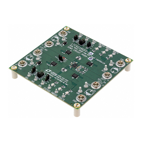
DESCRIPTION
Demonstration circuit 1899A controls two independent
power rail circuits each with Hot Swap™ and ideal diode
functionality provided by the LTC4228-1/LTC4228-2 dual
ideal diode and Hot Swap controller.
DC1899A facilitates evaluation of LTC4228 performance
in different operation modes such as supply ramp-up,
power supply switchover, steady state, and overcurrent
faults. Power supply switchover mode can be realized as
either an ideal diode or as a prioritizer.
Each DC1899A circuit is assembled to operate with a
12V supply and 9A maximum current load. The main
components of the board are the LTC4228 controller, two
MOSFETs operating as ideal diodes, two MOSFETs operat-
ing as Hot Swap devices, two current sense resistors, two
jumpers for independently enabling each rail, six LEDs to
PERFORMANCE SUMMARY
SYMBOL
PARAMETER
V
Input Supply Range
IN
V
Internal V
Undervoltage Lockout
INTVCC(UVL)
CC
V
Internal V
Undervoltage Lockout Hysteresis
INTVCC(HYST)
CC
Ideal Diode Control
ΔV
Forward Regulation Voltage (V
FWD(REG)
ΔV
External N-Channel Gate Drive
DGATE
(V
– V
)
DGATE
IN
I
CPO Pull-Up Current
CPO(UP)
I
DGATE Fast Pull-Up Current
DGATE(FPU)
I
DGATEn Fast Pull-Down Current
DGATE(FPD)
Hot Swap Control
ΔV
Circuit Breaker Trip Sense Voltage
SENSE(CB)
+
(V
– V
SENSEEn
SENSEEn
ΔV
Active Current Limit Sense Voltage
SENSE(ACL)
+
(V
– V
SENSEEn
SENSEEn
I
External N-Channel Gate Pull-Up Current
HGATE(UP)
I
External N-Channel Gate Pull-Down Current
HGATE(DN)
I
External N-Channel Gate Fast Pull-Down Current
HGATE(FPD)
Specifications are at T
CONDITIONS
INTV
– V
)
IN
OUT
ΔV
IN < 7V
IN = 7V to 18V
CPO = IN = 2.9V
CPO = IN = 18V
ΔV
ΔV
–
)
–
)
Gate Drive On, HGATE = 0V
Gate Drive Off, OUT = 12V, HGATE = OUT + 5V
Fast Turn-Off, OUT = 12V, HGATE = OUT + 5V
DEMO MANUAL DC1899A
LTC4228-1/LTC4228-2
Dual Ideal Diode and
Hot Swap Controller
indicate status, power good and fault conditions separately
for each channel, and input voltage snubbers. There are
pads for optional RC circuits for each Hot Swap MOSFET
gate in order to adjust output voltage slew rate. In addition
to this there are jumpers allowing monitoring of supply
undervoltage conditions at either IN or SENSE+ pins.
The standard configuration (as DC1899A populated by
default) places the ideal diode MOSFET ahead of the Hot
Swap MOSFET. The board also has pads for an alternative
configuration with the Hot Swap MOSFET located ahead
of the ideal diode MOSFET.
Design files for this circuit board are available at
http://www.linear.com/demo
L, LT, LTC, LTM, Linear Technology and the Linear logo are registered trademarks and
Hot Swap is a trademark of Linear Technology Corporation. All other trademarks are the
property of their respective owners.
= 25°C
A
Rising
CC
= 0.1V
FWD
= 0.2V, ΔV
= 0V, CPO = 17V
FWD
DGATE
= –0.2V, ΔV
= 5V
FWD
DGATE
MIN
TYP
MAX
UNITS
2.9
18
V
2.1
2.2
2.3
V
30
60
90
mV
10
25
40
mV
5
7
14
V
10
12
14
V
–60
–95
–120
μA
–50
–85
–110
μA
–1.5
A
1.5
A
47.5
50
52.5
mV
55
65
75
mV
–7
–10
–13
μA
150
300
500
μA
100
200
300
mA
dc1899af
1
Advertisement

Related Manuals for Linear Technology DC1899A


Summary of Contents for Linear Technology DC1899A
- Page 1 Hot Swap devices, two current sense resistors, two L, LT, LTC, LTM, Linear Technology and the Linear logo are registered trademarks and Hot Swap is a trademark of Linear Technology Corporation. All other trademarks are the jumpers for independently enabling each rail, six LEDs to property of their respective owners.
-
Page 2: Performance Summary
DEMO MANUAL DC1899A PERFORMANCE SUMMARY Specifications are at T = 25°C SYMBOL PARAMETER CONDITIONS UNITS Input/Output Pin ONn On Pin Threshold Voltage ON Rising 1.21 1.235 1.26 ON(TH) ONn Pin Fault Reset Threshold Voltage ON Falling 0.55 0.63 ON(RESET) EN Pin Threshold Voltage EN Rising 1.185... -
Page 3: Quick Start Procedure
Figure 1 for proper measurement equipment setup and in the three steps by the measuring of the transient’s follow the procedure below. The DC1899A test includes parameters in the different operation modes. independent tests of the LTC4228 Hot Swap functionality,... - Page 4 DEMO MANUAL DC1899A QUICK START PROCEDURE No-Load Rampup Current Limit Connect a 12V power supply to the board input turrets Initially adjust an electronic resistive load to 10Ω to 12Ω IN1 (IN2) and GND. Do not load the output. Place current and connect it to the OUT1 (OUT2) turret and GND.
- Page 5 PRIORITIZER FUNCTIONALITY TEST condition, but the LTC4228-2 automatically retries after 200ms to 450ms. The DC1899A is assembled with components to implement a power prioritizer with channel 1 having the higher priority. IDEAL DIODE FUNCTIONALITY TEST Place JP7 PPR_SEL (power priority select) jumper in position ON2 and JP5 RON2_SEL (ON2 select) in posi- Use an individual 12V power supply for each rail;...
- Page 6 DEMO MANUAL DC1899A PARTS LIST ITEM REFERENCE PART DESCRIPTION MANUFACTURER/PART NUMBER Required Circuit Components C1, C2, C3, C8, C9, C11, C14 CAP., X7R, 0.1μF, 50V, 0603 AVX, 06035C104KAT C4, C5 CAP., X7R, 47nF, 50V, 0603 AVX, 06035C473KAT C6, C7 CAP., X7R, 15nF, 50V, 0603...
-
Page 7: Schematic Diagram
Information furnished by Linear Technology Corporation is believed to be accurate and reliable. However, no responsibility is assumed for its use. Linear Technology Corporation makes no representa- tion that the interconnection of its circuits as described herein will not infringe on existing patent rights. - Page 8 Linear Technology Corporation (LTC) provides the enclosed product(s) under the following AS IS conditions: This demonstration board (DEMO BOARD) kit being sold or provided by Linear Technology is intended for use for ENGINEERING DEVELOPMENT OR EVALUATION PURPOSES ONLY and is not provided by LTC for commercial use. As such, the DEMO BOARD herein may not be complete in terms of required design-, marketing-, and/or manufacturing-related protective considerations, including but not limited to product safety measures typically found in finished commercial goods.
- Page 9 X-ON Electronics Largest Supplier of Electrical and Electronic Components Click to view similar products for category: Power Management IC Development Tools Click to view products by manufacturer: Analog Devices Other Similar products are found below : EVAL-ADM1168LQEBZ EVB-EP5348UI MIC23451-AAAYFL EV MIC5281YMME EV DA9063-EVAL ADP122-3.3-EVALZ ADP130- 0.8-EVALZ ADP130-1.2-EVALZ ADP130-1.5-EVALZ ADP130-1.8-EVALZ ADP1714-3.3-EVALZ ADP1716-2.5-EVALZ ADP1740-1.5- EVALZ ADP1752-1.5-EVALZ ADP1828LC-EVALZ ADP1870-0.3-EVALZ ADP1871-0.6-EVALZ ADP1873-0.6-EVALZ ADP1874-0.3- EVALZ ADP1882-1.0-EVALZ ADP199CB-EVALZ ADP2102-1.25-EVALZ ADP2102-1.875EVALZ ADP2102-1.8-EVALZ ADP2102-2-...
Need help?
Do you have a question about the DC1899A and is the answer not in the manual?
Questions and answers