
Related Manuals for MEIG SLM550


Summary of Contents for MEIG SLM550
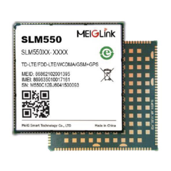
- Page 1 MeiG_SLM550_Hardware Design Manual MeiG SLM550 Hardware Design Manual Released Date: 2022/07/20 Version Number: V1.02 MeiG Smart Technology Co., Ltd 1/89...
-
Page 2: Important Notice
Copyright Notice All rights reserved. MeiG Smart Technology Co., Ltd This manual and all its contents are owned by MeiG Smart Technology Co., Ltd and protected by Chinese laws and relevant copyright laws in applicable international conventions. Without the written authorization of MeiG Smart Technology Co., Ltd, no one may copy, disseminate, distribute, modify or use part or all of this manual in any form, and the offenders will be held responsible according to law. -
Page 3: Revision History
2. Update microphone receiving circuit Figure 26. 3. BAT_THERM Pull-down resistor correct to 47K V1.02 2022-07-20 4. Update Table 6. 5. Update Figure 1, Figure 2, Figure 3. 6. MIPI impedance requirements 85 +/-15Ω. 7. Add FCC Statement. MeiG Smart Technology Co., Ltd 2/89... -
Page 4: Slm550 Hardware Design Guide _V1.02
MeiG_SLM550_Hardware Design Manual SLM550 Hardware Design Guide _V1.02 MeiG Smart Technology Co., Ltd 3/89... - Page 5 MeiG_SLM550_Hardware Design Manual Foreword Thank you for using the SLM550 module from Meg Smart. This product can provide data communication services. Please read the user manual carefully before use, you will appreciate its perfect function and simple operation method. The company does not assume responsibility for property damage or personal injury caused by improper operation of the user.
- Page 6 The end-product may need Verification testing, Declaration of Conformity testing, a Permissive Class II Change or new Certification. Please involve a FCC certification specialist in order to determine what will be exactly applicable for the end- product. MeiG Smart Technology Co., Ltd 5/89...
- Page 7 étiquette donnant le numéro de certification du module d'Industrie Canada, précédé des mots " Contient un module d'émission ", du mot IC:23860-SLM550 ou d'une formulation similaire exprimant le même sens, comme suit MeiG Smart Technology Co., Ltd...
- Page 8 Jusqu'à nouvel ordre, les équipements visés par la présente section ne peuvent pas être transférés sur la bande de 5 600 à 5 650 MHz, afin de protéger l'environnement des radars météorologiques exploités par le Canada surcette bande. MeiG Smart Technology Co., Ltd 7/89...
-
Page 9: Table Of Contents
MeiG_SLM550_Hardware Design Manual Contents Important Notice ............................1 Revision History ............................2 SLM550 Hardware Design Guide _V1.02 ....................3 Contents ..............................6 1 Introduction............................8 2 Module overview ..........................9 2.1 Summary of features ........................9 2.2 Block diagram ........................... 11 3 Module Package .......................... - Page 10 7.3 Humidity Sensitivity (MSL)......................79 7.4 Baking Requirements........................ 80 8 Support Peripheral Device List......................81 9 Appendix ............................83 9.1 Related Documents ........................83 9.2 Terms and Explanations......................83 9.3 Multiplexing function ......................... 85 9.4 Safety Warning.......................... 87 MeiG Smart Technology Co., Ltd 9/89...
-
Page 11: Introduction
RF interface. It can help users quickly understand the interface definition, electrical performance, and structural dimensions of the module. Combining this document with other application documents, users can quickly use modules to design mobile communication applications. MeiG Smart Technology Co., Ltd 10 /89... -
Page 12: Module Overview
MeiG_SLM550_Hardware Design Manual 2 Module overview SLM550 module uses the Qualcomm solution based on Arm Cortex-A53 Quad-core applications processor, with the highest main frequency of 4 * 2.0GHz, and the memory supports Dual-channel LPDDR4X SDRAM. This module is suitable for broadband intelligent wireless communication modules of TD-LTE/FDD-LTE/WCDMA/EVDO/TD-SCDMA/CDMA/GSM network standards. - Page 13 Camera Pixel: Max. Rear 13Mp/Front up to 13/25Mp Camera (Front and Rear) 1080p 30 fps: 8-bit H.264 Video decode 1080p 30 fps: 8-bit HEVC (H.265) , VP9 1080p 30 fps: 8-bit H.264 Video encode 1080p 30 fps: 8-bit HEVC (H.265) MeiG Smart Technology Co., Ltd 12/89...
-
Page 14: Block Diagram
2.4G +5G WiFi/BT antenna One main MIC One noise reduction MIC Audio One Handsfree speaker. One earpiece One stereo headphone. 2.2 Block diagram The following figure lists the main functional parts of the module: MeiG Smart Technology Co., Ltd 13/89... - Page 15 WIFI&BT Switch Duplex Duplex 2.4G WTR2965 16EM16- WCN3950 M4CTB29-GA70 VBAT Transceiver WIFI/BT eMCP PM4125 PWRKEY QCM2290 PMIC Baseband RESET_N ADCs STATUS USB (U)SIMx2 I2S UARTs GPIOs 38.4M VDD_1.8V Figure 4 Module function block diagram MeiG Smart Technology Co., Ltd 14/89...
-
Page 16: Module Package
ANT_MAIN USIM1_DATA USIM2_VDD CAM_I2C_SDA VIB_DRV_P CAM_I2C_SCL SCAM_PWDN SCAM_RST TP_INT TP_RST MCAM_PWDN SD_LDO4 MCAM_RST GPIO_108 UART2_TXD ANT_WIFI/BT UART2_RXD UART2_CTS SCAM_MCLK MCAM_MCLK UART2_RTS Signal Pins Power Pins GND Pins Figure 5 Module pin diagram (top view) MeiG Smart Technology Co., Ltd 15/89... -
Page 17: Pin Definitions
Comment The power supply The module provides Four Externally, large VBAT power pin pins. The capacito-rs and SLM550 operates from a VBAT 1, 2, 145, 146 Zener diodes single supply with a voltage must be added range from 3.4V to 4.2V for for surge protec- VBAT. - Page 18 (MIPI) DSI_CLK_N MIPI_LCD clock DSI_CLK_P DSI_LN0_N DSI_LN0_P DSI_LN1_N DSI_LN1_P MIPI_LCD data DSI_LN2_N DSI_LN2_P DSI_LN3_N DSI_LN3_P GPIO82_LCD0_RESE LCD reset GPIO81_LCD_TE LCD frame sync signal UART(1.8V) GPIO2_UART1_TXD UART1 data transmit GPIO3_UART1_RXD UART1 data receive MeiG Smart Technology Co., Ltd 17/89...
- Page 19 UIM1 data GPIO75_UIM2_DET UIM2 insert detect UIM2_RESET UIM2 reset UIM2_CLK UIM2 clock UIM2_DATA UIM2 data Front Camera CSI0_CLK_N Front Camera MIPI clock CSI0_CLK_P CSI0_LN0_N CSI0_LN0_P CSI0_LN1_N CSI0_LN1_P Front Camera MIPI data CSI0_LN2_N CSI0_LN2_P CSI0_LN3_N MeiG Smart Technology Co., Ltd 18/89...
- Page 20 Audio Interface MIC_GND The main MIC negative MIC_IN1_P The main MIC positive MIC_IN2_P Headphone MIC positive MIC_IN3_P Secondary MIC positive The BIAS voltage of main MIC_BIAS1 MIC is used in the design of silicon wheat MeiG Smart Technology Co., Ltd 19/89...
- Page 21 GPIO29_CAM_I2C_S Special I2C signal can only be used for CAM GPIO30_CAM_I2C_S GPIO22_DCAM_I2C_ SDA1 Pullup to Default for DCAM VREG_L15_1P8 GPIO23_DCAM_I2C_ SCL1 GPIO109_SENSOR_I 2C_SDA Special I2C signal can only GPIO110_SENSOR_I be used for SENSOR 2C_SCL MeiG Smart Technology Co., Ltd 20/89...
- Page 22 Generic GPIO, SPI MOSI GPIO14 Generic GPIO, SPI MISO GPIO17 Generic GPIO, SPI CS GPIO16 Generic GPIO, SPI CLK Generic GPIO, without GPIO105 default configuration The default configuration is GPIO34_MAG_INT the compass interrupt signal. MeiG Smart Technology Co., Ltd 21/89...
- Page 23 Generic GPIO, without GPIO101 default configuration Generic GPIO, without GPIO104 default configuration Generic GPIO, without GPIO36 default configuration Generic GPIO, without GPIO102 default configuration Generic GPIO, without GPIO108 default configuration Generic GPIO, without GPIO111 default configuration MeiG Smart Technology Co., Ltd 22/89...
- Page 24 PM215 is used, the pin shall be suspended. The charging indicator light CHG_LED negative GPIO91_KEY_VOL_U Control volume increase GPIO50_KEY_VOL_D Control volume decrease KYPD_PWR_N Pull down to power on / off RESET_N Pull down to reset MeiG Smart Technology Co., Ltd 23/89...
- Page 25 Default PM215 GPIO2 Grounding support power on CBL_PWR_N automatic startup BAT_ID Battery type detection 150, 151, 152, 173, 174, 175, 178, 179, 180, 183, 184, 192, RESERVED 232, 242, 246, 249, 252, 253, 254, 257, 263, MeiG Smart Technology Co., Ltd 24/89...
- Page 26 Configurable I/O,UIM2 removal UIM2_DET GPIO75* B-PD:nppukp detection UIM2_RESET B-PD:nppukp Configurable I/O,UIM2 reset UIM2_CLK B-PD:nppukp Configurable I/O,UIM2 clock UIM2_DATA B-PD:nppukp Configurable I/O,UIM2 data VREG_L19_UIM2 PMIC output for UIM2 Configurable I/O,UIM1 removal GPIO79_UIM1_DET GPIO79* B-PD:nppukp detection MeiG Smart Technology Co., Ltd 25/89...
- Page 27 BH-NP:pdpukp Secure digital controller 2 data bit SDC2_SDCARD_D2 BH-NP:pdpukp Secure digital controller 2 data bit SDC2_SDCARD_D3 BH-NP:pdpukp GPIO88_SD_CARD_ Configurable I/O,SD card GPIO88* B-PD:nppukp DET_N detection FORCED_USB_BOO pullup with VREG_L5 to forced GPIO95* USB boot MeiG Smart Technology Co., Ltd 26/89...
- Page 28 AI,AO lane0- MIPI camera serial interface 0 MIPI_CS1_LANE0_P AI,AO lane0+ MIPI_CSI1_LANE1_ MIPI camera serial interface 0 AI,AO lane1- MIPI_CSI1_LANE1_ MIPI camera serial interface 0 AI,AO lane1+ MIPI_CSI1_LANE3_ MIPI camera serial interface 1 AI,AO lane3- MeiG Smart Technology Co., Ltd 27/89...
- Page 29 RF signal for main ANT GPIO102 GPIO102 B-PD:nppukp Configurable I/O GPIO110_SENSOR_ Configurable I/O,SENSOR I2C GPIO110 B-PD:nppukp I2C_SCL GPIO109_SENSOR_ GPIO109 Configurable I/O,SENSOR I2C B-PD:nppukp I2C_SDA GPIO13_DBG_UART GPIO13* B-PD:nppukp Configurable I/O,UART2 RX GPIO12_DBG_UART GPIO12 B-PD:nppukp Configurable I/O,UART2 TX MeiG Smart Technology Co., Ltd 28/89...
- Page 30 GPIO107 B-PD:nppukp Configurable I/O KYPD_PWR_N KEY POWER ON/OFF GPIO105 GPIO105 B-PD:nppukp Configurable I/O GPIO16 GPIO16 B-PD:nppukp Configurable I/O, SPI CLK GPIO17 GPIO17* B-PD:nppukp Configurable I/O, SPI CS GPIO14 GPIO14* B-PD:nppukp Configurable I/O, SPI MISO MeiG Smart Technology Co., Ltd 29/89...
- Page 31 ADC BATT_THERM Battery temperature input to ADC CDC_HPH_R Headphone output, right channel CDC_HPH_REF Headphone ground reference CDC_HPH_L Headphone output, left channel MBHC mechanical CDC_HSDET_L insertion/removal-detection VBUS PI,PO USB Voltage VBUS PI,PO USB Voltage MeiG Smart Technology Co., Ltd 30/89...
- Page 32 PWDN Configurable I/O, depth CAM GPIO1 GPIO18_DCAM_RST B-PD:nppukp RESET GPIO20_DCAM_MC Configurable I/O, depth CAM B-PD:nppukp GPIO20 MCLK GPIO23_DCAM_I2C Configurable I/O, Dedicated B-PD:nppukp GPIO23 _SCL1 camera I2C1 SCL GPIO0 B-PD:nppukp Configurable I/O, I2C2 SDA GPIO0 MeiG Smart Technology Co., Ltd 31/89...
- Page 33 Reserved GPIO90 B-PD:nppukp Configurable I/O GPIO90* Reserved MIC1_INM Reserved MIC2_INM Reserved MIC3_INM NFC_CLK NFC CLK NFC_CLK_REQ DO-Z,DI Configurable I/O, NFC CLK REQ VPH_PWR Reserved VPH_PWR Reserved BAT_ID Battery ID CBL_PWR_N Cable power-on USB_CC1 Reserved MeiG Smart Technology Co., Ltd 32/89...
- Page 34 MIPI camera serial interface 0 AI,AO lane1+ MIPI_CSI0_LANE2_ MIPI camera serial interface 0 AI,AO lane2+ MIPI_CSI0_LANE3_ MIPI camera serial interface 0 AI,AO lane3+ GPIO111 B-PD:nppukp Configurable I/O GPIO111 GPIO22_DCAM_I2C Configurable I/O, Dedicated B-PD:nppukp GPIO22* _SDA1 camera I2C1 SDA MeiG Smart Technology Co., Ltd 33/89...
- Page 35 MeiG_SLM550_Hardware Design Manual RESET_N KEY RESET USB0_SS_TX1_P Reserved PM_GPI PM_GPIO8 B-PD:nppukp Only Configurable Out MeiG Smart Technology Co., Ltd 34/89...
- Page 36 Reserved Reserved Reserved Reserved USB0_SS_TX0_P Reserved USB0_SS_RX0_M Reserved USB0_SS_RX0_M USB0_SS_TX1_M Reserved GPIO62_RFFE5_CL B-PD:nppukp Configurable I/O,RFFE5 CLK GPIO62 GPIO61_RFFE5_DA B-PD:nppukp Configurable I/O,RFFE5 DATA GPIO61 Reserved B-PD:nppukp Configurable I/O GPIO41 GPIO41 B-PD:nppukp Configurable I/O GPIO40 GPIO40 MeiG Smart Technology Co., Ltd 35/89...
-
Page 37: Mechanical Dimensions
NP: pdpukp=defaultno-pull with programmable options following the colon (:) PD: nppukp=defaultpulldown with programmable options following the colon (:) PU: nppdkp=defaultpullup with programmable options following the colon (:) KP: nppdpu=defaultkeeper with programmable options following the colon (:) 3.3 Mechanical Dimensions MeiG Smart Technology Co., Ltd 36/89... - Page 38 MeiG_SLM550_Hardware Design Manual Figure 6 Module 3D size(unit :mm) Figure 7 Recommended PCB package size(unit :mm) MeiG Smart Technology Co., Ltd 37/89...
-
Page 39: Interface Application
Figure 8 VBAT input reference circuit If it is a DC power supply device, the DC input voltage is +5V. The recommended circuit that can be powered by DC-DC is shown below: Figure 9 DC-DC power supply circuit MeiG Smart Technology Co., Ltd 38/89... -
Page 40: Power Pin
The user can power on the module by pulling the KYPD_PWR_N pin (114) low. The pull-down time is at least 5 seconds. This pin has been pulled up to 1.8V in the module. The recommended circuit is as MeiG Smart Technology Co., Ltd 39/89... - Page 41 Figure 12 Using an external signal to drive the module to boot Figure 13 Booting with the button circuit The following figure is the boot timing description: Figure 14 Using PWRKEY boot timing diagram MeiG Smart Technology Co., Ltd 40/89...
-
Page 42: Module Shutdown
15 seconds. 4.2.3 Module Reset The SLM550 module supports a reset function that allows the user to quickly restart the module by pulling the RESET_N pin(225) of the module low. The recommended circuit is as follows: Figure 15 Reset using the key circuit Figure 16 Reset Module Using External Signal When the pin is high, the voltage is typically 1.8V. -
Page 43: Vcoin Power
RTC power supply uses an external large capacitor or battery to power the RTC inside the module: Figure 17 External Capacitor Powering the RTC Non-rechargeable battery powered: Figure 18 Non-rechargeable battery to power the RTC MeiG Smart Technology Co., Ltd 42/89... -
Page 44: Power Output
This VCOIN power supply is 2.0-3.25V, typical typically 3.0V 4.4 Power Output The SLM550 has multiple power outputs. For LCD, Camera, touch panel, etc. In application, it is recommended to add parallel 33PF and 10PF capacitors to each power supply to effectively remove high frequency interference. -
Page 45: Serial Port
MeiG_SLM550_Hardware Design Manual 4.5 Serial Port The SLM550 provides three serial ports for communication. And corresponding to one groups of I2C interfaces can be multiplexed into hardware flow control, note that the I2C interface can not be added to the UART_RTS/CTS when the pull resistor can be added. - Page 46 When using Levels Isolation in Figures 14 and 15, Attention should be paid to LDO6_1P8 output timing, the serial port can communicate normally after the normal output. Table 7 Serial Port Hardware Parameters Description Minimum Maximum Unit Input low level 0.63 Input high level 1.17 MeiG Smart Technology Co., Ltd 45/89...
-
Page 47: Mipi Interface
The total length should be as short as possible. 4.6.1 LCD Interface The SLM550 module Support 1 set of MIPI interface for LCD display, and has a compatible screen identification signal. The resolution of the screen can be up to 1680*720. The signal interface is shown in the following table. - Page 48 GPIO. MIPI is a high-speed signal line. To avoid EMI interference, it is recommended to place a common- mode inductor near the LCD side. Figure 23 LCD interface circuit MeiG Smart Technology Co., Ltd 47/89...
-
Page 49: Mipi Camera Interface
Figure 24 Backlight drive schematic 4.6.2 MIPI Camera Interface The SLM550 module supports the MIPI interface Camera and provides a dedicated camera power supply. The main camera is a CSI1 interface that supports four sets of data lines and can support up to 13M pixels. - Page 50 2.8V AVDD Extra LDO 1.2V DVDD Extra LDO 1.2V DVDD Sub camera interface Name Input/output Description MIPI_CSI0_CLK_M Sub camera MIPI clock signal MIPI_CSI0_CLK_P MIPI_CSI0_LANE0_M MIPI_CSI0_LANE0_P MIPI_CSI0_LANE1_M Sub camera MIPI data signal MIPI_CSI0_LANE1_P MIPI_CSI0_LANE2_M MIPI_CSI0_LANE2_P MIPI_CSI0_LANE3_M MeiG Smart Technology Co., Ltd 49/89...
- Page 51 Please pay attention to the length of the trace. It is not recommended to add a small capacitor on the MIPI signal line. This may affect the rising edge of the MIPI data. This in turn causes the MIPI data to be invalid. MeiG Smart Technology Co., Ltd 50/89...
- Page 52 MeiG_SLM550_Hardware Design Manual Figure 26 MIPI Camera Reference Circuit MeiG Smart Technology Co., Ltd 51/89...
-
Page 53: Capacitive Touch Interface
Description The capacitive touch I2C GPIO6_TP_I2C3_SDA interface needs to be pulled up GPIO7_TP_I2C3_SCL toVREG_L5_1P8 GPIO80_TP_INT_N TP Interrupt GPIO71_TP_RESET_N TP Reset VREG_L6_1P8 1.8V Power supply to TP I/O VREG_L17_2P8 2.8V Power supply to TP VDD MeiG Smart Technology Co., Ltd 52/89... -
Page 54: Audio Interface
MIC_BIAS3 BIAS voltage of the sub MIC for silicon CDC_HPH_R Headphone right channel CDC_HPH_L Headphone left channel CDC_HSDET_L Headphone plug detection CDC_HPH_REF Headphone reference ground EAR_M Earpiece output negative EAR_P Earpiece output positive MeiG Smart Technology Co., Ltd 53/89... -
Page 55: Receiver Interface Circuit
4.8.1 Receiver Interface Circuit Module Figure 28 Receiver Interface Circuit 4.8.2 Microphone receiving Circuit The figure below shows the interface circuit of MEMS microphone. Figure 29 Microphone Differential Interface Circuit 4.8.3 Headphone Interface Circuit MeiG Smart Technology Co., Ltd 54/89... -
Page 56: Line Out Circuit
4.8.5 I2S Interface There are a groups of GPIO-compatible I2S interfaces inside the module. The pins used by this function are as follows: Name Intput/Output Description GPIO100 I2S1 output DATA GPIO99 I2S1_ WS MeiG Smart Technology Co., Ltd 55/89... -
Page 57: Usb Interface
GPIO98 I2S1_ SLK 4.9 USB Interface The SLM550 supports a USB 2.0 High speed interface (Type-C optional). It must control the 90 ohm differential impedance during Layout and control the external trace length. The module supports OTG function. The voltage input range during charging is as follows:... - Page 58 MeiG_SLM550_Hardware Design Manual MeiG Smart Technology Co., Ltd 57/89...
-
Page 59: Usb Otg
MeiG_SLM550_Hardware Design Manual 4.9.1 USB OTG The SLM550 module can provide USB OTG function. The pins used in this function are as follows: Table 13 USB OTG Pin Description Pin name Description 5V charging input / OTG output power. VBUS... -
Page 60: Charging Detection
USB_DP/USB_DM. 4.10.2 Charge Control The SLM550 module can charge the over-discharged battery. The charging process includes trickle charge, pre-charge, constant current, and constant-voltage charge. When the VBAT voltage is lower than 3.4V, the module is pre-charged; when VBAT is between 3.4V and 4.2V, it is charged by the constant current plus constant voltage method optimized for the lithium battery. -
Page 61: Uim Card Interface
Figure 34 Charging circuit connection diagram 4.11 UIM Card Interface The SLM550 can support two SIM cards at the same time to achieve dual card dual standby. Support SIM card hot swap, can automatically recognize 1.8V and 3.0V cards. The figure below is the SIM recommended interface circuit. -
Page 62: Sd Card Interface
The reference circuit is as follows: Figure 36 SD Card Interface Circuit 4.13 I2C Bus Interface The SLM550 module supports five hardware I2C bus interfaces include two camera-specific CCI interface. The pin definitions and default functions are as follows: Table 14 I2C Interface Pin Description... -
Page 63: Analog To Digital Converter (Adc)
Gpio109 / 110 can only be used to connect sensor devices in Qualcomm QVL, no other devices. 4.14 Analog to Digital Converter (ADC) The SLM550 module provides two MPP function signals from the power management chip: PWM (29PIN) and ADC (128PIN), MPP can be configured as an ADC or PWM signal. -
Page 64: Motor
MeiG_SLM550_Hardware Design Manual 4.16 Motor The SLM550 supports motor functions and can be implemented by the user via PM_VIB_DRV_N (28PIN). The reference schematic diagram is as follows. Note that the uF-level capacitor cannot be placed on the signal line. Figure 37 Motor interface circuit 4.17 Antenna Interface... -
Page 65: Drx Antenna
In the figure, R102, C103, and C104 are antenna matching devices, and the specific component values can be determined after the antenna factory debugs the antenna. Among them, R102 defaults to 0R, C103 and C104 are not posted by default. MeiG Smart Technology Co., Ltd 64/89... -
Page 66: Gps Antenna
50 ohm microstrip line or strip line. In order to facilitate antenna debugging and certification testing, an RF connector and antenna matching network should be added. The recommended circuit diagram is as follows: MeiG Smart Technology Co., Ltd 65/89... - Page 67 Figure 44 WIFI_BT antenna interface simplified connection circuit In the above figure, R301 defaults to 0R, and C301 and C302 do not paste by default. MeiG Smart Technology Co., Ltd 66/89...
-
Page 68: Pcb Layout
SLM550 module is much higher than the previous 2G module, please read this chapter carefully, reduce the subsequent hardware debugging cycle. When using the SLM550 module, the user is required to use at least 4 layers of via holes for the PCB to facilitate impedance control and signal line shielding. -
Page 69: Power Supply
The GND processing must be performed on the upper and lower sides, and the traces are differential pairs. 100 ohm differential impedance matching is performed. Ensure impedance consistency and do not bridge different GND planes as MeiG Smart Technology Co., Ltd 68/89... -
Page 70: Usb
GSM antenna and VBAT during PCB layout and routing. The filter capacitor of the audio is preferably placed close to the module end and placed next to the interface end. The audio output should be routed according to the differential signal rules. MeiG Smart Technology Co., Ltd 69/89... -
Page 71: Safety Clearance
Therefore, there must be a safe distance between the module pads and other motherboard components. The recommended safe distance is 3mm. As shown below: MeiG Smart Technology Co., Ltd 70/89... -
Page 72: Electrical, Reliability
Table 18 Module Operating Temperature Parameter Minimum Typical Maximum Unit ℃ Working temperature ℃ Storage temperature 6.3 Working Voltage Table 19 Module Operating Voltage Parameter Minimum Typical Maximum Unit VBAT VBUS Hardware shutdown voltage MeiG Smart Technology Co., Ltd 71/89... -
Page 73: Digital Interface Features
Table 21 SIM_VDD Characteristics Parameter Minimum Typical Maximum Unit Description Output voltage Output current 6.6 PWRKEY Feature Table 22 PWRKEY Characteristics Parameter Description Minimum Typical Maximum Unit High level PWRKEY Low level 2000 Effective time MeiG Smart Technology Co., Ltd 72/89... -
Page 74: Vcoin Feature
FDD Standby power Ivbat consumption TDD Standby power consumption GSM900 CH62 32dBm Call Current consumption WCDMA2100 CH10700 22.5 dBm GPRS GSM900 CH62 PCL5 1DL 4UL Digital transmission EGPRS GSM900 CH62 PCL8 1DL 4UL MeiG Smart Technology Co., Ltd 73/89... -
Page 75: Electrostatic Protection
WCDMA B8 880~915MHz 925~960MHz RX: 2937~3088 CDMA BC0 869~894MHz 824~849MHz 1~799; 991~1023 TDSCDMA 1.9G 1880~1920 MHz 1880~1920MHz 9400~9600 TDSCDMA 2G 2010~2025 MHz 2010~2025MHz 10054~10121 TX: 18000~18599 LTE B1 2110~2170 MHz 1920~1980 MHz RX: 0~599 MeiG Smart Technology Co., Ltd 74/89... -
Page 76: Rf Characteristics
2496~2690 MHz 39650~41589 Note: The SLM550's LTE TDD B41 band bandwidth is 100MHz (2555 ~ 2655 MHz), the channel is 40040 ~ 41240. 6.11 RF Characteristics The following table lists the conducted RF output power of the module, in accordance with 3GPP TS 05.05 technical specification, 3GPP TS 134121-1 standard. -
Page 77: Module Conduction Receiving Sensitivity
1.4 MHz 3 MHz 5 MHz 10 MHz 15 MHz 20 MHz Duplex mode band number -100 -95.2 -102.7 -99.7 -93.2 -101.7 -98.7 -92.2 -104.7 -101.7 -100 -95.2 -103.2 -100.2 -100 -93.2 -102.2 -99.2 MeiG Smart Technology Co., Ltd 76/89... - Page 78 -95.2 -100 -101.2 -98.2 -96.5 -93.5 -91.7 -90.5 -102.7 -99.7 -97.5 -94.5 -92.7 -103.2 -100.2 -100.2 -98.5 -95.5 -93.7 -99.0 -95.7 -93.5 -100 -95.2 -100 -95.2 -106.2 -102.2 -100 -95.2 -106.2 -102.2 -100 -95.2 MeiG Smart Technology Co., Ltd 77/89...
-
Page 79: Wifi Main Rf Performance
Receiving performance(2.4G) Receiving sensitivity 802.11B 802.11G 802.11N Minimum rate Maximum rate Transmission performance(5G) 802.11A 802.11N 802.11AC Transmit power (minimum rate) Transmit power (maximum rate) EVM (maximum rate) Receiving performance(5G) 802.11AC Receiving sensitivity 802.11A 802.11N (20M) MeiG Smart Technology Co., Ltd 78/89... -
Page 80: Bt Main Rf Prformance
Table 31 Main RF performance parameters under GNSS conduction GNSS working frequency band: 1575.42MHZ GNSS carrier-to-noise ratio CN0: 40dB/Hz Capture (cold start) Capture (hot start) Track GNSS sensitivity: -148 -156 -160 Hot start Warm start Cold start GNSS startup time MeiG Smart Technology Co., Ltd 79/89... -
Page 81: Production
MeiG_SLM550_Hardware Design Manual 7 Production 7.1 Top And Bottom Views Of The Module Figure 45 Module top and bottom views MeiG Smart Technology Co., Ltd 80/89... -
Page 82: Recommended Soldering Furnace Temperature Curve
Figure 46 Module recommended soldering furnace temperature curve 7.3 Humidity Sensitivity (MSL) The SLM550 module meets moisture sensitivity level 3. The dry package is subjected to the J-STD- 020C specification in accordance with the IPC/JEDEC standard under ambient conditions of temperature <30 ℃... -
Page 83: Baking Requirements
90°C and as high as 125°C 7.4 Baking Requirements Due to the humidity sensitivity of the module, the SLM550 should be thoroughly baked prior to reflow soldering, otherwise the module may cause permanent damage during reflow soldering. The SLM550 should be baked for 192 hours in a cryogenic vessel at 40°C +5°C/-0°C and a relative humidity of less... -
Page 84: Support Peripheral Device List
Vendor Drive IC Specification GOODiX GT5688 5" Table 37 Support for G Sensor Model List Vendor Model Specification Bosch BMI120 9-axis,16bit/16bit Table 38 Support for Ecompass Model List Vendor Model Specification GMEMS GMC303 3-Axis,14-bit MeiG Smart Technology Co., Ltd 83/89... - Page 85 MeiG_SLM550_Hardware Design Manual Table 39 Support PS/ALS Sensor Model List Vendor Model Specification LITEON LTR-553ALS-01 ALS+PS Table 40 Support for Gyro Sensor Model List Vendor Model Specification Bosch BMI120 9-axis,16bit/16bit MeiG Smart Technology Co., Ltd 84/89...
-
Page 86: Appendix
GSM 11.10 (MS) conformance specification; Part 1:Conformance specification AN_Serial Port AN_Serial Port 9.2 Terms and Explanations Table 42 Terms and explanations Terms Explanations Analog-to-Digital Converter Adaptive Multi-Rate Coding Scheme Circuit Switched Data Clear to Send MeiG Smart Technology Co., Ltd 85/89... - Page 87 Password Authentication Protocol PBCCH Packet Broadcast Control Channel Printed Circuit Board Power Control Level Personal Communication System, also referred to as GSM 1900 Protocol Data Unit Point-to-point protocol Radio Frequency Root Mean Square (value) MeiG Smart Technology Co., Ltd 86/89...
-
Page 88: Multiplexing Function
Mobile Equipment list of received calls SIM phonebook Not connect 9.3 Multiplexing function Table 43 Multiplexing Functions Reuse function GPIO Module pin UART GPIO_0 SPI_MISO UART_CTS I2C_SDA GPIO_1 SPI_MOSI UART_RTS I2C_SCL GPIO_2 SPI_SCLK UART_TXD MeiG Smart Technology Co., Ltd 87/89... - Page 89 TP_INT_N. 3. GPIO12, GPIO13 default used for Debug_UART, GPIO96 default used for KEY_VOL_UP and GPIO97 default used for KEY_VOL_DOWN. Blue is the default function simultaneous UART, and I2C functionality are not supported in SLM550. MeiG Smart Technology Co., Ltd 88/89...
-
Page 90: Safety Warning
Pay attention to the following safety precautions when using or repairing any terminal or mobile phone that contains modules. The user should be informed of the following safety information on the terminal device. Otherwise, Meig will not be responsible for any consequences caused by the user not following these warning actions.
Need help?
Do you have a question about the SLM550 and is the answer not in the manual?
Questions and answers