Table of Contents

Related Manuals for MEIG SLM758


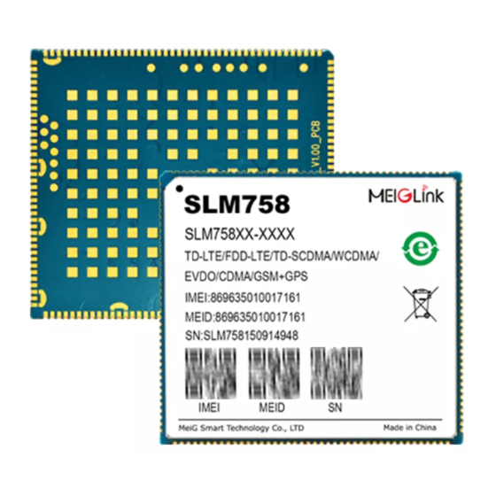
Summary of Contents for MEIG SLM758
- Page 1 MeiG Smart product technical information SLM758 Hardware Design Guide Released Date: 2018/11 File name: SLM758 Hardware Design Guide Version Number: V1.08 Company: MeiG Smart Technology Co., Ltd SLM758 Hardware Design Guide Page 1...
- Page 2 DISCLAIMER MeiG Smart will not take any responsibility for any property and health damage caused by the abnormal operation of customers. Please develop the product according to the technical specification and designing reference guide which defined in the product manual. MeiG Smart have the right to modify the document according to technical requirement with no announcement to the customer.
- Page 3 MeiG Smart product technical information SLM758 Hardware Design Guide _V1.08 SLM758 Hardware Design Guide Page 3...
- Page 4 MeiG Smart product technical information Foreword Thank you for using the SLM758 module from Meg Smart. This product can provide data communication services. Please read the user manual carefully before use, you will appreciate its perfect function and simple operation method.
-
Page 5: Table Of Contents
MeiG Smart product technical information Contents Introduction ................................8 Module overview ..............................8 2.1 Summary of features ............................ 10 2.2 Block diagram ............................. 12 3. Module Package ..............................13 3.1.Pin distribution diagram ..........................13 3.2. Pin definitions .............................. 14 3.3. Mechanical Dimensions ..........................30 4. - Page 6 MeiG Smart product technical information 6. Electrical, Reliability ............................. 67 6.1 Absolute Maximum ............................67 6.2 Working Temperature..........................67 6.3 Working Voltage ............................67 6.4 Digital Interface Features..........................67 6.5 SIM_VDD Characteristics .......................... 68 6.6 PWRKEY Feature ............................68 6.7 VCOIN Feature ............................68 6.8 Current Consumption (VBAT = 3.8V) .......................
- Page 7 MeiG Smart product technical information Version History Date Version Change description Author 2017-06-12 1.00 First edition Zheng Lei 2017-08-15 1.01 Correction Guo Qianghua 2017-11-01 1.02 Modify information Zheng Lei 2017-11-01 1.03 Modify information Zheng Lei 2018-1-5 1.04 Modify information Zheng Lei...
-
Page 8: Introduction
2. Module overview SLM758 series core board, uses the MSM8953 of Qualcomm Snapdragon 600 series for its main chip, and its CPU is made of 14nm FinFET, built in 64bit ARM, 8 cores Cortex A-53, main frequency 2.0G processor, supporting LPDDR3 SDRAM memory. - Page 9 MeiG Smart product technical information The SLM758 provides voice, SMS, address book, WiFi, BT and GPS functions while providing high-speed broadband data access; Product supports dual 1300W 3D camera or depth of field camera, and it can be widely used in VR Camera, intelligent robot, Video surveillance, security, automotive equipment, intelligent platform handheld terminals and other products.
-
Page 10: Summary Of Features
MeiG Smart product technical information 2.1 Summary of features Table 2.1: SLM758 features Product characteristics Description Plateform Qualcomm MSM8953 Octa-core A53 (64bit) 8*2.0GHz * Octa-core A53 (64bit) 8*1.8GHz * Octa-core A53 (64bit) 8*2.2GHz Adreno506;650MHz System memory 16GB eMMC + 2GB LPDDR3 933Mhz compatible with 32GB+3GB Android 7.1... - Page 11 MeiG Smart product technical information 13MP Camera at the same time 4K 30fps, 1080p 60fps, H.264/H.265 MP4/ WMV9/ Video decode VC1/ DivX/ VP8/VP9 4K 30fps,1080p 60 fps: H.264/ H.265/ MP4/ VP8 Video encode 1080P 60fps De +1080p 30fps En Key(Power on/off, Home, Volume+, Volume-)...
-
Page 12: Block Diagram
MeiG Smart product technical information 2.2 Block diagram The following figure lists the main functional parts of the module: MSM8953 baseband chip PM8953 power management chip PMI8952 power management chip WCN3660B(Compatible with WCN3680B)-WIFI/BT/FM three in one chip ... -
Page 13: Module Package
MeiG Smart product technical information Figure 2.1: module function block diagram 3. Module Package 3.1.Pin distribution diagram SLM758 Hardware Design Guide Page 13... -
Page 14: Pin Definitions
MeiG Smart product technical information Figure 3.1:module pin diagram (top view) 3.2. Pin definitions table 3.1:Pin description Pin number Pin number Description Comment The power supply SLM758 Hardware Design Guide Page 14... - Page 15 MeiG Smart product technical information The module provides three Externally, VBAT power pin pins. The capacitors and VBAT 151、152、153 SLM758 operates from a single Zener diodes supply with a voltage range must be added from 3.4V to 4.2V for VBAT. for surge VBUS 5V charging input power.
- Page 16 MeiG Smart product technical information Main display interface (MIPI) MIPI_DSI0_CLK_N MIPI_LCD clock MIPI_DSI0_CLK_P MIPI_DSI0_LANE0_N MIPI_DSI0_LANE0_P MIPI_DSI0_LANE1_N MIPI_DSI0_LANE1_P MIPI_LCD data MIPI_DSI0_LANE3_N MIPI_DSI0_LANE3_P MIPI_DSI0_LANE2_N MIPI_DSI0_LANE2_P GPIO61_LCD_RST_N LCD reset GPIO24_LCD_TE0 LCD frame sync signal The main display backlight interface Each normal LCD_BL_LED_K1 LCD Series backlight negative1 20mA,max...
- Page 17 MeiG Smart product technical information GPIO16_UART5_TX UART5 data transmit GPIO21_UART6_RX UART6 data receive GPIO20_UART6_TX UART6 data transmit UIM card Interface UIM1_DET UIM1 insert detect UIM1_RESET UIM1 reset UIM1_CLK UIM1 clock UIM1_DATA UIM1 data UIM2_DET UIM2 insert detect UIM2_RESET UIM2 reset...
- Page 18 MeiG Smart product technical information MIPI_CSI0_LANE3_P GPIO26_MCAM_MCLK Rear Camera main clock GPIO40_MCAM_RST_N Rear Camera reset GPIO39_MCAM_PWD_N Rear Camera dormancy Depth Camera MIPI_CSI1_CLK_N Depth Camera clock MIPI_CSI1_CLK_P MIPI_CSI1_LANE0_N MIPI_CSI1_LANE0_P MIPI_CSI1_LANE1_N MIPI_CSI1_LANE1_P Depth Camera MIPI data MIPI_CSI1_LANE2_N MIPI_CSI1_LANE2_P MIPI_CSI1_LANE3_N MIPI_CSI1_LANE3_P GPIO132_DCAM_PWD_N Depth Camera dormancy...
- Page 19 MeiG Smart product technical information Power amplifier (0.85 W) output SPKR_DRV_P Class_D positive SD card Interface GPIO133_SDCARD_DET_N SD card insertion detection SDC2_SDCARD_CMD SD CMD SDC2_SDCARD_CLK SD clock SDC2_SDCARD_D0 SDC2_SDCARD_D1 SD data SDC2_SDCARD_D2 SDC2_SDCARD_D3 CAM_I2C_SDA0 Special I2C signal can only be...
- Page 20 MeiG Smart product technical information GPIOand default function GPIO0_SPI_MOSI GPIO1_SPI_MISO The default configuration is the SPI interface GPIO2_SPI1_CS GPIO3_SPI1_CLK Generic GPIO, without default GPIO8 configuration Generic GPIO, without default GPIO9 configuration Generic GPIO, without default GPIO33 configuration Generic GPIO, without default...
- Page 21 MeiG Smart product technical information General purpose GPIO, no GPIO128 default configuration GPIO138_FP_SPI_MISO The default configuration is SPI GPIO137_FP_SPI_MOSI interface for fingerprint GPIO136_FP_SPI_CS recognition. GPIO135_FP_SPI_CLK Other functional pin Pull up to 1.8 V FORCE_USB_BOOT (VREG_L5_1P8) into the emergency download mode...
- Page 22 MeiG Smart product technical information FLASH_LED1+ FLASH LED anode(1A) PMI8952_MPP1 AO-Z,AI,DO Configurable MPP,PWM,ADC LCD_BL_LED_K1 LCD Backlight cathode1(20mA) LCD_BL_LED_K2 LCD Backlight cathode2(20mA) LCD_BL_LED_A LCD Backlight anode PMI_HAP_OUT_N Haptics driver output negative PMI_HAP_OUT_P Haptics driver output positive UART2_MSM_TX GPIO_4 B-PD:nppukp Configurable I/O,UART2 TX...
- Page 23 MeiG Smart product technical information SDC2_SDCARD_D3 Secure digital controller 2 data bit 3 NP:pdpukp SDC2_SDCARD_CMD Secure digital controller 2 command NP:pdpukp SDC2_SDCARD_CLK Secure digital controller 2 clock NP:pdpukp MIPI_CSI2_CLK_P MIPI camera serial interface 2 clock+ MIPI_CSI2_CLK_N MIPI camera serial interface 2 clock-...
- Page 24 MeiG Smart product technical information MIPI_DSI0_LANE2_N MIPI display serial interface 0 lane2- MIPI_DSI0_LANE2_P MIPI display serial interface 0 lane2+ MIPI_DSI0_LANE3_N MIPI display serial interface 0 lane3- MIPI_DSI0_LANE3_P MIPI display serial interface 0 lane3+ Configurable I/O, primary GPIO61_LCD_RST_N GPIO_61* B-PD:nppukp RESET...
- Page 25 MeiG Smart product technical information Configurable I/O, Dedicated camera CAM_I2C_SCL0 B-PD:nppukp I2C0 SCL Configurable I/O, Dedicated camera CAM_I2C_SDA0 B-PD:nppukp I2C0 SDA Configurable I/O,UIM1 removal GPIO54_UIM1_DET GPIO_54* B-PD:nppukp detection UIM1_RESET B-PD:nppukp Configurable I/O,UIM1 reset UIM1_CLK B-PD:nppukp Configurable I/O,UIM1 clock UIM1_DATA B-PD:nppukp Configurable I/O,UIM1 data...
- Page 26 MeiG Smart product technical information VREG_L10_2P8_SENSOR PMIC output 2.8V for sensor PMIC output 1.8V for LCD,CAM,TP, VREG_L6_1P8 sensor VREG_L5_1P8 PMIC output 1.8V for digital I/Os PM_RESIN_N1 KEY VOL-(default) or RESET KYPD_PWR_N1 KEY POWER ON/OFF USB_ID USB ID USB_HS_D_M AI,AO USB data minus...
- Page 27 MeiG Smart product technical information USB super-speed receive – minus USB3_SS_RX_M USB super-speed receive – plus USB3_SS_RX_P GPIO20_UART6_TX GPIO_20 B-PD:nppukp Configurable I/O,UART6 TX GPIO21_UART6_RX GPIO_21* B-PD:nppukp Configurable I/O,UART6 RX Reserved Reserved Reserved Reserved CHG_LED Current sink for charging indication Reserved...
- Page 28 MeiG Smart product technical information boot MIPI_CSI1_CLK_N MIPI camera serial interface 1 clock- MIPI_CSI1_CLK_P MIPI camera serial interface 1 clock- PM8953_MPP4 AO-Z,DI,DO Configurable MPP,PWM,ADC GPIO66 GPIO_66 B-PD:nppukp Configurable I/O VREG_L13_3P075 PMIC output 3.075V for audio codec VREG_S4_2P05 PMIC output 2.05V for audio codec...
- Page 29 MeiG Smart product technical information MIPI_DSI1_LANE1_P MIPI display serial interface 1 lane1+ MIPI_DSI1_LANE1_N MIPI display serial interface 1 lane1- MIPI_DSI1_CLK_P MIPI display serial interface 1 clock+ MIPI_DSI1_CLK_N MIPI display serial interface 1 clock- MIPI_DSI1_LANE2_P MIPI display serial interface 1 lane2+...
-
Page 30: Mechanical Dimensions
MeiG Smart product technical information *:Wake-up system interrupt pin B:Bidirectionaldigital with CMOS input H:High-voltage tolerant NP:pdpukp=defaultno-pull with programmable options following the colon (:) PD:nppukp=defaultpulldown with programmable options following the colon (:) PU:nppdkp=defaultpullup with programmable options following the colon (:) KP:nppdpu=defaultkeeper with programmable options following the colon (:) 3.3. -
Page 31: Interface Application
MeiG Smart product technical information Figure 3.2:Module 3D size(unit :mm) 4. Interface application 4.1. Power Supply SLM758 Hardware Design Guide Page 31... - Page 32 MeiG Smart product technical information In the case of a battery device, the voltage input range of the module VBAT is 3.4V to 4.2V, and the recommended voltage is 3.8V. In the GSM band, when the module is transmitting at maximum power, the peak current can reach up to 3A, resulting in a large voltage drop on VBAT.
-
Page 33: Power Pin
MeiG Smart product technical information Figure 4.2:DC-DC power supply circuit Note:If the user does not use battery power, please note that a 10K resistor is connected to the 149 pin (BAT_THERM) of the module and pulled down to GND to prevent the software from judging the abnormal battery temperature after the module is turned on, resulting in shutdown. -
Page 34: Power On And Off
MeiG Smart product technical information attention to the design of the power supply section to ensure that the VBAT does not fall below 3.4V even when the module consumes 2A. If the voltage drops below 3.4V, the module may shut down. The PCB layout from the VBAT pin to the power supply should be wide enough to reduce the voltage drop in the transmit burst mode. -
Page 35: Module Shutdown
MeiG Smart product technical information Figure 4.6:Booting with the button circuit The following figure is the boot timing description: Figure 4.7:Using PWRKEY boot timing diagram 4.2.2. Module Shutdown Users can use the PWRKEY pin to shutdown. 4.2.2.1 PWRKEY Shutdown SLM758 Hardware Design Guide... -
Page 36: Module Reset
15 seconds. 4.2.3.Module Reset The SLM758 module supports a reset function that allows the user to quickly restart the module by pulling the RESET pin of the module low. The recommended circuit is as follows: Figure 4.8:Reset using the key circuit Figure 4.9:... -
Page 37: Vcoin Power
MeiG Smart product technical information 3.3V, it is not possible to directly use the GPIO of the MCU to drive the pin. An isolation circuit is required. The hardware parameters of the RESET can refer to the following table: Table 4.1:RESET Hardware Parameters... -
Page 38: Power Output
This VCOIN power supply is typically 3.0V and consumes approximately 3uA when VBAT is disconnected. 4.4. Power Output The SLM758 has multiple power outputs. For LCD, Camera, touch panel, etc. In application, it is recommended to add parallel 33PF and 10PF capacitors to each power supply to effectively remove high frequency interference. - Page 39 MeiG Smart product technical information Name Direction Function UART2_MSM_TX UART2 Data Transmission UART2_MSM_RX UART2 Data Reception UART2 Clear To Send GPIO6_I2C2_SDA (CTS) UART2 Request To Send GPIO7_I2C2_SCL (RTS) GPIO12_UART4_TX UART4 Data Transmission GPIO13_UART4_RX UART4 Data Reception UART4 Clear To Send GPIO14_SENSOR_I2C4_SDA (CTS)...
- Page 40 MeiG Smart product technical information level shifting IC, the following figure can also be used to achieve level matching. Only the matching circuits on TX and RX are listed here. Other low speed signals can refer to this two circuits.
-
Page 41: Mipi Interface
(Refer to the MIPI Alliance Specfication for D-PHY 7.6.5). 4.6.1. LCD Interface The SLM758 module supports the MIPI interface of two LCD displays, supports dual- screen display, and has a compatible screen identification signal. The resolution of the screen can be up to 1920*1200. The signal interface is shown in the following table. In the Layout, the MIPI signal line should strictly control the differential 100 ohm impedance and the equal length between the signal line group and the group. - Page 42 MeiG Smart product technical information Main screen interface MIPI_DSI0_CLK_N MIPI_LCD clock line MIPI_DSI0_CLK_P MIPI_DSI0_LANE0_N MIPI_DSI0_LANE0_P MIPI_DSI0_LANE1_N MIPI_DSI0_LANE1_P MIPI_LCD data line MIPI_DSI0_LANE3_N MIPI_DSI0_LANE3_P MIPI_DSI0_LANE2_N MIPI_DSI0_LANE2_P GPIO61_LCD_RST_N LCD reset pin GPIO24_LCD_TE0 LCD frame sync signal LCD series backlight negative LCD_BL_LED_K1 pole 1...
- Page 43 MeiG Smart product technical information the internal circuit of LCD. If the internal divider of the LCD uses resistor divider, please pay attention to the voltage to meet the high or low range of GPIO. MIPI is a high-speed signal line. To avoid EMI interference, it is recommended to place a common-mode inductor near the LCD side.
- Page 44 MeiG Smart product technical information Figure 4.16:Main LCD and sub LCD interface circuit Both the primary and secondary LCDs require a backlight circuit. The backlight of the main LCD is driven inside the module. It can directly use LCD_BL_LED_A, LCD_BL_LED_K1, LCD_BL_LED_K2 to support up to 2 strings of 8 LEDs in total.
-
Page 45: Mipi Camera Interface
GPIO. 4.6.2.MIPI Camera Interface The SLM758 module supports the MIPI interface Camera and provides a dedicated camera power supply. The main camera is a CSI0 interface that supports four sets of data lines and can support up to 24M pixels. The front camera is a CSI2 interface that supports four sets of data lines and can support 8M pixels. - Page 46 MeiG Smart product technical information Front camera interface Name Input/output Description MIPI_CSI2_CLK_P Front camera MIPI clock signal MIPI_CSI2_CLK_N MIPI_CSI2_LANE0_P MIPI_CSI2_LANE0_N MIPI_CSI2_LANE1_P MIPI_CSI2_LANE1_N Front camera MIPI data signal MIPI_CSI2_LANE2_P MIPI_CSI2_LANE2_N MIPI_CSI2_LANE3_P MIPI_CSI2_LANE3_N Front camera clock signal GPIO27_SCAM_MCLK Front camera reset signal...
- Page 47 MeiG Smart product technical information If the user designs to use the CAMERA module with autofocus function, please note that the I2C of the module cannot be directly connected to the AF device. The I2C of the AF device should be connected to the driver chip of CAMERA, and the correct connection is as follows: Figure 18:...
- Page 48 MeiG Smart product technical information Figure 4.19:MIPI Camera Reference Circuit Important note: When designing the camera function, you need to pay attention to the position of the connector. There will be a small person in the specification of the camera to indicate the imaging direction.
-
Page 49: Resistive Touch Interface
MeiG Smart product technical information 4.7.Resistive Touch Interface The module does not provide a resistive touch screen interface. If the user needs to use a resistive touch, an external dedicated chip is required. The module can provide an I2C interface. -
Page 50: 1Receiver Interface Circuit
MeiG Smart product technical information CDC_HPH_L Headphone left channel CDC_HS_DET Headphone plug detection CDC_HPH_REF Headphone reference ground CDC_EAR_M Earpiece output negative CDC_EAR_P Earpiece output positive SPKR_DRV_M Amplifier (0.85W) output negative SPKR_DRV_P Amplifier (0.85W) output positive Users are advised to use the following circuit according to the actual application to get better sound effects. -
Page 51: Headphone Interface Circuit
MeiG Smart product technical information Figure 4.22: Microphone Differential Interface Circuit 4.9.3.Headphone Interface Circuit The module integrates a stereo headphone jack. Users are advised to reserve ESD devices during the design phase to prevent ESD damage. The HS_DET pin of the module can be set as an interrupt. -
Page 52: Speaker Interface Circuit
MeiG Smart product technical information 2. We recommend that the headphone detection pin HS_DET and HPH_L form a detection circuit (the connection method in the above figure), because HPH_L has a pull-down resistor inside the chip, which can ensure that HS_DET is low when connected with HPH_L, if the user will HS_DET and HPH_R To connect, please reserve a 1K pull-down resistor on HPH_R. -
Page 53: I2S Interface
GPIO135_FP_SPI_CLK 4.10. USB Interface The SLM758 supports a USB 2.0 /3.0High/Super speed interface. It must control the 90 ohm differential impedance during Layout and control the external trace length. The module supports OTG function at the same time and can output 5V/1A current. -
Page 54: Usb Otg
MeiG Smart product technical information Figure 4.26: USB Connection Diagram 4.10.1. USB OTG The SLM758 module can provide USB OTG function. The pins used in this function are as follows: Table 4.10: USB OTG Pin Description Pin name Description 5V charging input / OTG output power. -
Page 55: Charging Interface
MeiG Smart product technical information 4.11. Charging Interface The SLM758 module integrates a 2A charging solution. The charging related content of this manual is only described by the internal charging scheme. The MSM8953 platform uses the Qualcomm PMI8952 internal integrated charging chip by default. The chip is in switching mode and has high efficiency. -
Page 56: Uim Card Interface
Figure 4.29: Charging circuit connection diagram 4.12 UIM Card Interface The SLM758 can support two SIM cards at the same time to achieve dual card dual standby. Support SIM card hot swap, can automatically recognize 1.8V and 3.0V cards. The figure below is the SIM recommended interface circuit. -
Page 57: Sd Card Interface
The reference circuit is as follows: Figure 4.31: SD Card Interface Circuit 4.14 I2C Bus Interface The SLM758 module supports four hardware I2C bus interfaces and one camera-specific CCI interface. The pin definitions and default functions are as follows: Table 4.11: I2C Interface Pin Description... -
Page 58: Analog To Digital Converter (Adc)
4.17. Motor The SLM758 supports motor functions and can be implemented by the user via PMI_HAP_OUT_N (8PIN) and PMI_HAP_OUT_P (9PIN). The reference schematic diagram is as follows. Note that the uF-level capacitor cannot be placed on the signal line. -
Page 59: Antenna Interface
MeiG Smart product technical information 4.18 Antenna Interface The module provides four antenna interfaces: MAIN antenna, DRX antenna, GPS antenna and WiFi/BT antenna. In order to ensure that the user's products have good wireless performance, the antenna selected by the user should meet the requirement that the input impedance is 50 ohms in the working frequency band and the VSWR is less than 2. -
Page 60: Drx Antenna
MeiG Smart product technical information 4.18.2 DRX Antenna The module provides the DRX antenna interface pin RF_DIV, and the antenna on the user's motherboard should be connected to the module's antenna pins using a 50-ohm characteristic microstrip or stripline. In order to facilitate antenna debugging and certification testing, an RF connector and antenna matching network should be added. -
Page 61: Gps Antenna
MeiG Smart product technical information 4.18.3 GPS Antenna The module provides the GNSS antenna pin RF_GPS. The antenna on the user's main board should be connected to the antenna pin of the module using a 50-ohm characteristic microstrip line or strip line. - Page 62 MeiG Smart product technical information If there are fewer components between the antenna and the module output, or if the RF test head is not needed in the design, the antenna matching circuit can be simplified as shown below: Figure 4.41: WIFI_BT antenna interface simplified connection circuit In the above figure, R301 defaults to 0R, and C301 and C302 do not paste by default.
-
Page 63: Pcb Layout
2G module, please read this chapter carefully, reduce the subsequent hardware debugging cycle. When using the SLM758 module, the user is required to use at least 4 layers of via holes for the PCB to facilitate impedance control and signal line shielding. -
Page 64: Power Supply
MeiG Smart product technical information The device and wiring between the antenna pin and the antenna connector of the module must be away from high-speed signal lines and strong interference sources to avoid crossing or parallel with any signal lines in adjacent layers. -
Page 65: Mipi
MeiG Smart product technical information 5.2.4. MIPI MIPI is a high-speed signal line. Users must pay attention to protection during the layout stage, so that they are away from the signal lines that are easily interfered. The GND processing must be performed on the upper and lower sides, and the traces are differential pairs. -
Page 66: Other
MeiG Smart product technical information the TDD interference of the DCS1800 frequency band is more serious. Therefore, the user can select the required filter capacitor according to the actual test result, and sometimes even do not need to paste the filter capacitor. -
Page 67: Electrical, Reliability
MeiG Smart product technical information 6. Electrical, Reliability 6.1 Absolute Maximum The table below shows the absolute maximum values that the module can withstand. Exceeding these limits can cause permanent damage to the module. Table 6.2: Absolute Maximum Parameter Minimum... -
Page 68: Sim_Vdd Characteristics
MeiG Smart product technical information 6.5 SIM_VDD Characteristics Table 6.5: SIM_VDD Characteristics Parameter Description Minimum Typical Maximum Unit Output voltage Output current 6.6 PWRKEY Feature Table 6.6: PWRKEY Characteristics Parameter Description Minimum Typical Maximum Unit High level PWRKEY Low level... -
Page 69: Electrostatic Protection
MeiG Smart product technical information current GSM Standby power consumption WCDMA Standby power consumption TD-S Standby power consumption CDMA Standby power consumption FDD Standby power consumption 4.45 TDD Standby power consumption Call GSM900 CH62 32dBm Current consumpt WCDMA2100 CH10700 22.5 dBm... - Page 70 1880~1920 MHz 1880~1920 MHz 38250~38649 LTE B40 2300~2400 MHz 2300~2400 MHz 38650~39649 LTE B41 2496~2690 MHz 2496~2690 MHz 39650~41589 Note: The SLM758's LTE TDD B41 band bandwidth is 100MHz (2555 ~ 2655 MHz), the SLM758 Hardware Design Guide Page 70...
-
Page 71: Rf Characteristics
MeiG Smart product technical information channel is 40240 ~ 41240. 6.11 RF Characteristics The following table lists the conducted RF output power of the module, in accordance with 3GPP TS 05.05 technical specification, 3GPP TS 134121-1 standard. Table 6.10: Conducted Output Power... -
Page 72: Wifi Main Rf Performance
MeiG Smart product technical information -100 -93.2 -102.2 -99.2 -94.2 -100 -95.2 -100 -101.7 -98.7 -100 -95.2 -100 -95.2 -91.2 -100 -95.2 -92.2 -104.7 -101.7 -100 -95.2 -100 -101.2 -98.2 -96.5 -93.5 -91.7 -90.5 -102.7 -99.7 -97.5 -94.5 -92.7 -103.2 -100.2... -
Page 73: Bt Main Rf Prformance
MeiG Smart product technical information Receiving sensitivity 802.11B 802.11G 802.11N Minimum rate Maximum rate Transmission performance(5G) 802.11A 802.11N 802.11AC Transmit power (minimum rate) Transmit power (maximum rate) EVM (maximum rate) Receiving performance(5G) 802.11AC Receiving sensitivity 802.11A 802.11N (20M) Minimum rate -88.5... -
Page 74: Production
Figure 49: Module recommended soldering furnace temperature curve 7.3. Humidity Sensitivity (MSL) The SLM758 module meets moisture sensitivity level 3. The dry package is subjected to the J-STD-020C specification in accordance with the IPC/JEDEC standard under ambient conditions of temperature <30 degrees and relative humidity <60%. Under ambient... -
Page 75: Baking Requirements
The SLM758 should be baked for 192 hours in a cryogenic vessel at 40° C +5° C/- 0° C and a relative humidity of less than 5%, or in a high temperature vessel at 80° C± 5° C.Bake for 72 hours. -
Page 76: Support Peripheral Device List
MeiG Smart product technical information 8. Support Peripheral Device List Peripheral devices can support the devices included in the platform QVL. The following are the software default adapters. Table 8.1: List of supported display models Vendor Drive IC Specification Zoneway... - Page 77 MeiG Smart product technical information GMEMS GMC303 3-Axis,14-bit Table 8.6: Support PS/ALS Sensor Model List Vendor Model Specification LITEON LTR-553ALS-01 ALS+PS Table 8.7: Support for Gyro Sensor Model List Vendor Model Specification Bosch BMI120 9-axis,16bit/16bit Table 8.8: Peripheral Support List...
-
Page 78: Appendix
MeiG Smart product technical information 9. Appendix 9.1. Related Documents Table 9.1: Related documents Serial numb File name Comment Digital cellular telecommunications (Phase 2+); AT command set for GSM GSM 07.07: Mobile Equipment (ME) Support GSM 07.10 multiplexing protocol GSM 07.10:... - Page 79 MeiG Smart product technical information Li-ion Lithium-Ion Mobile Originated Mobile Station (GSM engine), also referred to as TE Mobile Terminated Password Authentication Protocol PBCCH Packet Broadcast Control Channel Printed Circuit Board Power Control Level Personal Communication System, also referred to as GSM 1900...
-
Page 80: Multiplexing Function
MeiG Smart product technical information 9.3. Multiplexing function Table 9.3: Multiplexing Functions Reuse function Module GPIO UART MOSI MISO CS_N MOSI MISO CS_N MOSI MISO CS_N MOSI MISO CS_N MOSI MISO CS_N MOSI MISO CS_N MOSI MISO CS_N MOSI MISO... -
Page 81: Safety Warning
Pay attention to the following safety precautions when using or repairing any terminal or mobile phone that contains modules. The user should be informed of the following safety information on the terminal device. Otherwise, Meig will not be responsible for any consequences caused by the user not following these warning actions. -
Page 82: End Product Labeling
If not, a second label must be placed on the outside of the final device that contains the following text: “Contains FCC ID: 2APJ4-SLM758”... -
Page 83: Federal Communication Commission Interference Statement
MeiG Smart product technical information 10.4.Federal Communication Commission Interference Statement This device complies with Part 15 of the FCC Rules. Operation is subject to the following two conditions: (1) This device may not cause harmful interference, and (2) this device must accept any interference received, including interference that may cause undesired operation. -
Page 84: Radiation Exposure Statement
This equipment complies with FCC/IC radiation exposure limits set forth for an uncontrolled environment. This equipment should be installed and operated with minimum distance 20 cm between the radiator & your body. Shenzhen MeiG Technology Technology Co., Ltd. Shanghai Branch Add:3/F,No.88,Qinjiang Road,Xuhui District,Shanghai...
Need help?
Do you have a question about the SLM758 and is the answer not in the manual?
Questions and answers