Table of Contents
Advertisement
Quick Links
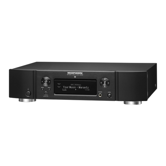
NETWORK AUDIO PLAYER
NA6006
• For purposes of improvement, specifications and design are subject to change without notice.
• Please use this service manual when referring to the operating instructions without fail.
• Some illustrations used in this service manual are slightly different from the actual product.
Service Manual
Click here!
On-line service parts list
http://dmedia.dmglobal.com/Document/DocumentDetails/24925
ONLINE PARTS LIST
(P5)
WEB owner's manual
NA:
http://manuals.marantz.com/NA6006/NA/EN/index.php
EU:
http://manuals.marantz.com/NA6006/EU/EN/index.php
AP: http://manuals.marantz.com/NA6006/AP/ZH/index.php
JP:
http://manuals.marantz.com/NA6006/JP/JA/index.php
Upload is planned for the time of a future press release.
BEFORE SERVICING THIS UNIT
ELECTRICAL
MECHANICAL
REPAIR INFORMATION
UPDATING
Confidential
Ver. 1
Advertisement
Table of Contents

Related Manuals for Marantz NA6006


Summary of Contents for Marantz NA6006
- Page 1 Click here! NA6006 On-line service parts list http://dmedia.dmglobal.com/Document/DocumentDetails/24925 ONLINE PARTS LIST (P5) WEB owner’s manual http://manuals.marantz.com/NA6006/NA/EN/index.php http://manuals.marantz.com/NA6006/EU/EN/index.php AP: http://manuals.marantz.com/NA6006/AP/ZH/index.php http://manuals.marantz.com/NA6006/JP/JA/index.php Upload is planned for the time of a future press release. BEFORE SERVICING THIS UNIT ELECTRICAL MECHANICAL REPAIR INFORMATION UPDATING • For purposes of improvement, specifications and design are subject to change without notice.
- Page 2 BEFORE SERVICING THIS UNIT SAFETY PRECAUTIONS NOTE FOR SCHEMATIC DIAGRAM HANDLING THE SEMICONDUCTOR AND OPTICS ONLINE PARTS LIST Accessing the Parts List Searching Part Numbers or Ref. Numbers NOTE FOR PARTS LIST SERIAL NUMBER Serial Number Organization SKU Code of this Unit POST-SERVICE PRECAUTIONS Initializing this Unit...
-
Page 3: Safety Precautions
SAFETY PRECAUTIONS The following items should be checked for continued protection of the customer and the service technician. Leakage current check Before returning the set to the customer, be sure to carry out either (1) a leakage current check or (2) a line to chassis resistance check. If the leakage current exceeds 0.5 milliamps, or if the resistance from chas- sis to either side of the power cord is less than 460 kohms, the set is defective. -
Page 4: Note For Schematic Diagram
NOTE FOR SCHEMATIC DIAGRAM WARNING: Parts indicated by the z mark have critical characteristics. Use ONLY replacement parts recommended by the manufacturer. CAUTION: Before returning the set to the customer, be sure to carry out either (1) a leakage current check or (2) a line to chassis resistance check. -
Page 5: Note For Parts List
ONLINE PARTS LIST Accessing the Parts List Searching Part Numbers or Ref. Numbers (1) Access from the Service Manual You can search a Parts List for part numbers or Ref. numbers. ・ Click the URL link on the cover of the service manual. (1) Enter the part number or Ref. - Page 6 The 14-digit serial number that contains the code of the manufacturing plant and the manufacturing date. 14 digits Factory Manufactured Cumulative Year, month code code serial number The last Month 2digit of year (01 ~ 12) SKU Code of this Unit Product SKU SKU Code NA6006/N1B NA6006/FN NA6006/K1B NA6006/N1SG NA6006/U1B...
-
Page 7: Initializing This Unit
POST-SERVICE PRECAUTIONS Initializing this Unit Make sure to initialize this unit after replacing the microcomputer or any peripheral equipment, or the PCB. 1. Press the power operation button to turn off the power, and remove the AC plug from the socket. 2. -
Page 8: Schematic Diagrams
ELECTRICAL SCHEMATIC DIAGRAMS SCH01 CPU SCH02 DIR SCH03 PLD SCH04 NETWORK SCH05 AUDIO SCH06 HP SCH07 FRONT SCH08 POWER SCH09 SMPS PRINTED CIRCUIT BOARDS FRONT, HEADPHONE, POWER SW, WI-FI ANT L GUIDE, WI-FI ANT R GUIDE, FFC GUIDE, POWER AUDIO, MAIN SMPS BLOCK DIAGRAM POWER DIAGRAM... - Page 9 SCHEMATIC DIAGRAMS SCH01 CPU P3V3_D P5V_D_USB P3V3_UCOM L3002 C3017 P3V3_UCOM CB05YTYH221-2012 4.7UF-K-1608 HP_GAIN_M HP_GAIN_H C3020 C3025 100N-K 100N-K D3000 LBAS16HT1G-2012 TO 0A CN3003 CN3003 GND_D 12P WAFER U3000 C_DSD_PHASE_MODE C3031 C3041 C3054 NJM2845DL1-18 4.7UF-K-1608 4.7UF-K-1608 4.7UF-K-1608 C_PLD_DAC1_MUTE P3V3_D P1V8_D P3V3_UCOM C_PCM_DSD_MODE +3.3V_CPU C3042...
- Page 10 SCH02 DIR P5V_D_SPDIF P3V3_D C3085 L3005 C3095 P3V3_D_AUDIO 4.7UF-K-1608 4.7UF-K-1608 P3V3_D P3V3_D_AUDIO CB05YTYH221-2012 P1V8_D C3087 C3090 100N-K 100N-K P5V_D_SPDIF GND_D P5V_D_AUDIO GND_D GND_D_AUDIO P5V_D_A N5V_D_A TO A2 I2C_SCL_DIR2 I2C_SDA_DIR2 I2C_SCL_DAC2 I2C_SDA_DAC2 DAC2_RESET C3164 100N-K DIR_DIN U3010 DIR_DOUT JST2165 U3011 DIR_CE TC7WHU04FU-TRB DIR_CLK R3232...
- Page 11 SCH03 PLD C3173 L3009 4.7UF-K-1608 P3V3_D_PLD P3V3_D P3V3_D_PLD CB05YTYH221-2012 C3170 100N-K GND_D GND_D GND_D P1V8_D C3198 P1V8_D P1V8_D 100N-K C3197 TO A1 OPEN R3307 I2C_SDA_CS2K R3318 OPEN TO A5 OPEN I2C_SDA_CS2K I2C_SCL_CS2K R3317 OPEN I2C_SCL_CS2K R3302 OPEN CS2K_PLD_MCK GND_D PLD_SRC_MCK P3V3_D_PLD SRC_PLD_PBCK/DBCK PLD_SRC_CM0...
- Page 12 SCH04 NETWORK NETWORK L3015 P3V3_UCOM CB05YTYH221-2012 LEGO5V P5V_NET LEGO5V P5V_D_USB C3216 C3218 R3332 100N-K 100N-K GND_D R3331 GND_D R3325 C3208 100N-K TO A0 Q3012 Q3014 RT1N441C FDC608PZ GND_D L3014 CB05YTYH221-2012 NET3.3V NET3.3V C3215 C3217 R3330 100N-K 100N-K R3329 100K GND_D R3324 C3207 100N-K...
- Page 13 SCH05 AUDIO CN2000 +5VA +5VA GND_A GND_A GND_A +3V3_DAC +3_3DAC +3V3_D1 +3_3D1 B2000 B2000_1 +1V3_DAC +1_3D1 +12V_A_FIXED GND_A +12V_A 2P WIRE B2000_2 +12V_A D2014 GND_DA D2022 1SS302A 1SS302A -12V_A -12V_A GND_A P_MUTE P_MUTE GND_A R2108 TO CN1000 CN2000 82(AX) C2079 1000PF(FNS) C2080 1000PF(FNS) U2006 11P WAFER...
- Page 14 SCH06 HP CN2001_ TO _CN2001 TO H/P B'D R2276 0-1608 R2277 0-1608 R2278 0-1608 CN2001 C2065 100N-K 5 6 7 8 9 10 10P WAFER R2246 R2244 R2245 GND2001 +12V_HP -12V_HP +12V_A R2238 100(1) +3_3D1 +12V_A +12V_HP_ R2239 100(1) -12V_HP_ Q2055 RT1P141C Q2110...
- Page 15 SCH07 FRONT FRONT OLED UNIT CP120 TO CP1004 MAIN POWER BLOCK CP119 TO CN3002 FROM MAIN PART CP120 7P WIRE C342 100N-K CP119 1.0-11S-27PW RMC100 C343 R302S8-5T 100N-K R528 +3.3V_CPU C344 100N-K GND_D REMOTE__ REMOTE_ D136 LBAS16HT1G L140 CB05YTYH221 Vout Vout Vadj Control...
- Page 16 SCH08 POWER CP1004 F1005 T1AL/250V CP1004 D1044 LBAS16HT1G 20010WS-07 PROTECT D1023 D1029 D1021 D1032 +3.3V_CPU +3.3V_CPU 1SR154-3216 1SR154-3216 1SR154-3216 1SR154-3216 +3.3V_D +3.3V_D +18V_OLED D1020 D1022 D1028 D1031 +18V_OLED +18V_OLED +18V_OLED 1SR154-3216 1SR154-3216 1SR154-3216 1SR154-3216 GND_D GND_D GND_D TO CP120 GND_D GND_D GND_A GND_D...
- Page 17 SCH09 SMPS T811 T811 CN441 CN441 EE1916(MT19165V) EE1916(MT19165V) 20010WS-11 20010WS-11 RLY_PWRA C805 C805 R811 R811 C811 C811 D801 D801 D802 D802 47uF 47uF 330K 330K 103K 103K RELAY 1N4007 1N4007 C803 C803 C804 C804 1N4007 1N4007 400V 400V 630V 630V SD102M SD102M SD102M...
-
Page 18: Printed Circuit Boards
FRONT, HEADPHONE, POWER SW, WI-FI ANT L GUIDE, WI-FI ANT R GUIDE, FFC GUIDE, POWER Lead-free Solder When soldering, use the Lead-free Solder (Sn-Ag-Cu). FRONT (A SIDE) FRONT (B SIDE) J205 S110 NA6006 FRONT(MP) R432 L141 J201 C342 7020-08284-000-0S C323... - Page 19 R3081 R3192 R3193 C3089 NET_PLD_MCK. Q2029 R3086 C3157 C3056 PLD_DIR1_MCK C2029 C3070 U3013 5M570ZF256C5N C2031 U2004 R3085 R3241 ADC_PLD_PBCK. NA6006 AUDIO PCB(MP) KIA7907PI R3090 Q2009 R2095 DIR2_PLD_DATA. R3235 ADC_PLD_LRCK. D2024 R3094 C3159 R3261 R3239 ADC_PLD_DATA. Q2056 10/50(KR3) DIR2_PLD_LRCK. C2052 7020-08282-040-0V...
- Page 20 SMPS SMPS (A SIDE) SMPS (B SIDE)
-
Page 21: Block Diagram
BLOCK DIAGRAM NA6006 AUDIO DIAGRAM DIR2_I2S 5M570ZF256C5N (PLD) SPDIF OUT1 DIR_I2S DIR_I2S SPDIF OPT IN I/V CONVERTER HDAM AMP I/V CONVERTER ES9016K2M (MAIN DAC) PCM/DSD DATA/BCK/LRCK ANALOG L/R I2S-1 I/V CONVERTER HDAM AMP I/V CONVERTER I2S-0 TC74LCX157FU NJU72343 80MHz (SWITCH) -
Page 22: Power Diagram
POWER DIAGRAM NA6006 VCC DIAGRAM MAIN TRANS DISPLAY (DC19.7V) (DC0.2A) +3V3_CPU +3V3_CPU P3V3_UCOM DIGITAL +3V3_CPU NET3.3V (DC7.66V) (DC0.6A) +3.3V_D +3.3V_D P3V3_D_AUDIO +3.3V_D P3V3_D_PLD +3.3V_D P1V8_D P5V_NET LEGO5V NETWORK (DC5.72V) (DC0.9A) P5V_D_USB P5V_D_SPDIF (DC6.09V) (DC1.0A) P5V_D_USB P5V_D_AUDIO P5V_D_A P5V_D_OPA D_AUDIO (DC6.34V) (DC0.2A) -
Page 23: Wiring Diagram
WIRING DIAGRAM NA6006 WIRING DIAGRAM MAIN PCB LEGO MODULE AUDIO PCB SMPS PCB POWER PCB MAIN TRANS H/P PCB FRONT PCB POWER S/W PCB... - Page 24 SEMICONDUCTORS Only major semiconductors are shown, general semiconductors etc. are omitted to list. The semiconductor which described a detailed drawing in a schematic diagram are omitted to list. 1. IC's R5F5631FDDFB (DIGITAL : U3001) Pin Name Port Name MODE SNTB Function Net- Nomal...
- Page 25 P50/TXD2 DAC_CLK_SEL O O/L DAC Input MCK Select (80MHz(H) or Power Supply Pin 45MHz/49MHz(L)) PA4/TXD5/IRQ5-DS RC_OUT O/L NA6006 only, DNP800 is Open. Ground Pin Ground Pin DAC1_MUTE O/L DAC1 (Fixed Out, Variable Out, H/P Out) PA3/RXD5/IRQ6-DS DIR_DIN O/L DIR (PCM9211) Control Pin...
- Page 26 NAME DGV or PW DW or N Address inputs 0 through 2. Connect directly to V or ground. Pullup 112 P64 RESERVED NA6006 Open A[0..2] 6, 7, 9 6, 7, 9 1, 2, 3 resistors are not needed. — Ground...
- Page 27 *For adjustable version only. AK4458VN 40 +105 C (Exposed pad is connected to ground) Figure 1. Typical Application Circuit 40 +85 C (Exposed pad is open) Figure 1. Typical Application Circuit 48-pin QFN (0.5mm pitch) AKD4458 Evaluation Board for AK4458 NCP380 (MAIN : U3017) AK4458VN (MAIN : U3006) Pin Configurations...
- Page 28 [AK4458] FUNCTIONAL BLOCK DIAGRAM No. Pin Name I/O Function PD State 4. Block Diagram and Functions CAD0_I2C Chip Address 0 Pin in I2C Bus serial control mode Chip Select Pin in 3-wire serial control mode LDOE TVDD VDD18 DVSS AVDD AVSS Hi-Z Audio Data Format Select in Parallel control mode.
- Page 29 PCM9211 PCM9211 (MAIN : U3007) www.ti.com SBAS495 – JUNE 2010 PIN CONFIGURATIONS DESCRIPTION NAME PT PACKAGE LQFP-48 TOLERANT (TOP VIEW) MS/ADR1 Software control I/F, SPI chip select / I2C slave address setting1(2) MODE Control mode setting, (see the Serial Control Mode section, ERROR/INT0 VDDRX Control Mode Pin Setting)
- Page 30 PCM9211 PCM9211 BLOCK DIAGRAM LC89091JA (MAIN : U3009) www.ti.com SBAS495 – JUNE 2010 BLOCK DIAGRAM FILT AUXIN 0 AUTO RXIN7 RXIN 0 RXIN0 SCKO DOUT RXIN 1 RXIN1 MAIN OUTPUT RXIN 2 RXIN2 AUXIN0 LRCK SCKO/ BCK/LRCK PORT RXIN 3 RXIN3 AUXIN1 DOUT...
- Page 31 ES9016K2M (AUDIO : U2002) NJU72343_J (AUDIO : U2007) DGND DVDD N.C. DGND ES9016K2M N.C. DVCC 28-QFN ADDR VCCA AVCCDAC XI (MCLK) N.C. No. Symbol Function No. Symbol Function AREF Analog reference potential DATA IC control data input Address selection CLOCK IC control clock input PIN DESCRIPTIONS InA2...
-
Page 32: Oled Display
2. OLED DISPLAY MXS4035A MXS4035A IO Interfaces... - Page 33 VOLUME ▲ VOLUME ▼ QUEUE <= BACK <= OPTION <= Extended Code SETUP <= NA6006 must receive following codes. ▲ (UP) <= These codes are not included in the RC005NA ▼ (DOWN) <= RC-5/RC-5 Ext. (LEFT) <= Name System Command...
- Page 34 MECHANICAL DISASSEMBLY Flowchart 1. FRONT PANEL ASSY 2. MAIN PCB 3. SMPS PCB 4. POWER PCB 5. AUDIO PCB EXPLODED VIEW PACKAGING VIEW...
- Page 35 DISASSEMBLY Flowchart • Remove each part following the flow below. • Reassemble the removed parts in the reverse order. • Read "SAFETY PRECAUTIONS" before reassembling the removed parts. • If wire bundles are removed or moved during adjustment or part replacement, reshape the wires after completing the work. Failure to shape the wires correctly may cause problems such as noise. • See "EXPLODED VIEW" TOP COVER FRONT PANEL ASSY MAIN PCB SMPS PCB POWER PCB AUDO PCB DISASSEMBLY DISASSEMBLY DISASSEMBLY DISASSEMBLY DISASSEMBLY 1. FRONT PANEL ASSY 2. MAIN PCB 3. SMPS PCB 4. POWER PCB 5. AUDIO PCB and "EXPLODED VIEW" and "EXPLODED VIEW" and "EXPLODED VIEW" and "EXPLODED VIEW" and "EXPLODED VIEW" FRONT PCB MAIN PCB SMPS PCB POWER PCB AUDIO PCB...
-
Page 36: Front Panel Assy
Explanatory Photos for DISASSEMBLY 1. FRONT PANEL ASSY • For the shooting direction of each photos used in this manual, see the photo below. Proceeding : TOP COVER → FRONT PANEL ASSY • A, B, C and D in the photo below indicate the shooting directions of photos. • The photographs with no shooting direction indicated were taken from the top of the unit. (1) Remove the screws. • Photos of NA6006N1SG are used in this manual. The viewpoint of each photograph (Shooting direction : X) [View from the top] ↓Shooting direction: B↓ View from the bottom (2) Remove the connector wire and FFC. Remove the screws. - Page 37 2. MAIN PCB 3. SMPS PCB Proceeding : TOP COVER → SMPS PCB Proceeding : TOP COVER → MAIN PCB (1) Remove the screws. (1) Remove the screws. (2) Remove the screws. Remove the connector wire and FFC. (2) Remove the screws. Remove the connector wire and FFC. Antenna connector CN441 MAIN PCB CN802 SMPS PCB CN801 4. POWER PCB Proceeding : TOP COVER →...
- Page 38 5. AUDIO PCB Proceeding : TOP COVER → AUDIO PCB (1) Remove the screws. (2) Remove the screws. Remove the connector wire and FFC. GND Terminal CN2001 CN2000 AUDIO PCB CN2002...
-
Page 39: Exploded View
EXPLODED VIEW http://dmedia.dmglobal.com/Document/DocumentDetails/24925 Parts List : S2x2 S11x1 S11X7 S8x4 S3x1 S10x3 S10x1 S1x9 S6x1 S9x2 S6x2 S3x1 S6x4 S3x4 S4x4 P7-1 S5x2 P7-2 S10x3 S3x2 S3x1 S3x5 S3x2 S3x1 S3x4 P1-4 P1-1 S2x1 S3x1 P1-2 P1-3 S2x2 S3x1 S2x5 S3x2 S3x1 S2x1... - Page 40 PACKAGING VIEW http://dmedia.dmglobal.com/Document/DocumentDetails/24925 Parts List : UK plug (UK Only) NA6006 Manual packing style CARD PASS Bag,Poly(Zipper) NOTES ON RADIO Caution on Using Batteries(N only) Safety sheet Warranty CANADA(U only) Warranty USA(U only) Sheet,AWA(F only) Sheet,SPOTIFY(N&U only) User card(F only)
-
Page 41: Repair Information
REPAIR INFORMATION TROUBLE SHOOTING 1. POWER 2. OLED 3. No Remote Control Reception 4. Audio PCB Abnormalities and no Audio Output (Line Out, Variable Out, H/P Out) 5. No Audio Output during USB File Playback (USB input), File Playback on a Server or Internet Radio and Bluetooth Playback 6. - Page 42 TROUBLE SHOOTING 1. POWER 1.1. The unit does not power on Check that the LED is lit (when connected to the Check the Protection history. Can the "Protection History" be checked? AC inlet). [DC PROTECTION1] Does the POWER indicator blink in red immedi- ("1-3.
- Page 43 1.3. Power Supply Voltage Abnormalities POWER PCB Check the output voltage. POWER PCB to MAIN PCB Is there an abnormality in any of the power supply ICs? Replace any faulty parts. [CN3003 : 1pin] = +3.3 ± 0.5V, +3.3V_CPU If the input voltage of all the power supply ICs is 0V, proceed to Or replace the POWER PCB.
- Page 44 2. OLED 2.1. OLED is not lit Checking the Digital communication waveform Check that the connection is correct and after starting the power supply. The MCU is malfunctioning or latched. Check the cable and its connection. reconnect FFC. FRONT PCB [CP119 : 13-24pin] Check each part listed after "1.4.
- Page 45 3. No Remote Control Reception Check that you are using a [RC005NA] remote control and replace the batteries. Check the Square wave signal. Can a square wave be found? FRONT PCB[Q518] Collector。 Change the setting of the [REMOTE CONTROL] Is the [REMOTE CONTROL] switch on the back Point the remote control at the unit and check .
- Page 46 4. Audio PCB Abnormalities and no Audio Output (Line Out, Variable Out, H/P Out) This section details items to check if the digital audio signal is being correctly input to the Audio PCB DAC IC [U2002]. Check the Clock. Check the Clock. Output terminal of crystal oscillator [X2000] AUDIO PCB の...
- Page 47 Check the audio signal. Check the output signal. There may be an abnormality in the combined differential at a Set "Variable Out" and "Phones" to ON in "Audio" in the menu AUDIO PCB point after the I/V conversion circuit. settings. Are signals output from all of the I/V converter circuit outputs (4 Refer to the circuit diagram and check for open parts or a short Line Out, Variable Out, H / P Out output terminal.
- Page 48 5. No Audio Output during USB File Playback (USB input), File Playback on a Server or Internet Radio and Bluetooth Playback Before testing circuit operation, check if the file to be played back is in a supported format and network settings are correct. Check output of digital audio waveform.
- Page 49 6. No Audio Output during OPT Playback Check the following areas to identify the area where the S/PDIF Check the S/PDIF input signal. signal is cut off. MAIN PCB Malfunctions in the OPT INPUT terminal DIR[U3007], [R3151] OPT IN Power supply voltage of input buffer IC[U3011], input/output Check output of digital audio waveform during playback of OPT input signal.
- Page 50 7. Audio is not output from OPT OUT Check the following areas to identify the area where the S/PDIF Check the S/PDIF output signal. signal is cut off. MAIN PCB Malfunctions in the OPT INPUT terminal DIR[U3007], [R3232] OPT OUT Power supply voltage of input buffer IC[U3011], input/output Check input of digital audio waveform.
- Page 51 MEASURING METHOD AND WAVEFORMS 1. MAIN PCB test point Check playback from the applicable input source. (It is recommended to use extension wires between the probe and test points.) MAIN PCB : test point q PCM/DSD_BCK w PCM_WCK/DSDL e PCMDATA/DSDR r DIR1_PLD_PBCK t DIR1_PLD_LRCK y DIR1_PLD_DATA...
- Page 52 WAVEFORMS 1-3 DAC input PCM PBCK_LRCK_DATA 4-6 Digital input playback PCM PBCK_LRCK_DATA r DIR1_PLD_PBCK q PCM t DIR1_PLD LRCK w PCM_WCK y DIR1_PLD_DATA e PCMDATA 7-9 Network playback PCM PBCK_LRCK_DATA 10-12 DIT input PCM_BCK_LRCK_DATA Q0 PLD_DIT_PBCK u NET_PLD_I2S0_BCK Q1 PLD_DIT_LRCK i NET_PLD_I2S0_LRCK Q2 PLD_DIT_DATA oNET_PLD_I2S0_DATA...
-
Page 53: Special Mode Setting Button
SPECIAL MODE Special mode setting button b No. 1: Insert the AC plug while pressing button "A", and wait for more than 3 seconds. b No. 2 - 4: Insert the AC plug while pressing buttons "A" and "B" together, and wait for more than 3 seconds. b No. - Page 54 1. Selecting the Mode1 for Service-related 1.1. Actions Selecting Each Mode. 1.2. Starting up Insert the AC plug while pressing button "POWER", and wait for more than 3 seconds. Release button "POWER" when the power indicator turns green. Executes an update for the entire device via DPMS. Select the desired mode using the "CURSOR f / d "...
-
Page 55: Version Display Mode
o HEOS Restore 1-1. Version Display Mode 1-1.1. Actions Version information is displayed when the device is started in this mode. 1-1.2. Starting up Q0 Ether Mac Address Insert the AC plug while pressing button "POWER", and wait for more than 3 seconds. Release button "POWER"... -
Page 56: Protection History Display Mode
・ Display when protection has been activated 1-2. IR Control Test This function is used to check IR control operations. 1-2.1. Starting up Insert the AC plug while pressing button "POWER", and wait for more than 3 seconds. Cause : Power supply short circuit detected in the power supply board Release button "POWER"... - Page 57 1-5. Initialize Initializes all MCU and network module backup data. NOTE: If initialization is executed in LEGO Off mode, cancel LEGO off mode then reset the LEGO Net- work. 1-5.1. Starting up Insert the AC plug while pressing button "POWER", and wait for more than 3 seconds. Release button "POWER"...
- Page 58 2. Factory Initialization Mode 4. Firmware Factory Restore Initialize backup data of the MCU. Used when replacing the Network module. "3. Update method when the MAIN PCB or network module is replaced (Using a USB flash drive 2.1. Starting up U3001, U3013, NETWORK MODULE)"...
- Page 59 (3) When saving of the log package fails, "USB Failed" appears in the display for 5 seconds, regardless of 6. Selecting the Mode2 for Service-related whether the upload to the server was successful. Selecting Each Mode. 6.1. Starting up While the power is on, hold down buttons "POWER" and "ENTER" for at least 3 seconds. (1) "LEGO Log Capture Mode"...
- Page 60 UPDATING PROCEDURE AFTER REPLACING THE PCB. PROCEDURE AFTER REPLACING THE U-COM, ETC. FIRMWARE UPDATE PROCEDURE 1. Items necessary for update 2. Update preparation with a USB flash drive (U3001, U3013, NETWORK MODULE) 3. Update method when the MAIN PCB or network module is replaced (Using a USB flash drive U3001, U3013, NETWORK MODULE) 4.
- Page 61 PROCEDURE AFTER REPLACING THE PCB. PROCEDURE AFTER REPLACING THE U-COM, ETC. The procedure after replacing the printed circuit boards is as follows. The procedure after replacing the u-COM (microprocessor) is as follows. (1) Change the resistor for setting the region. Implement the update method when the MAIN PCB or network module is replaced.
-
Page 62: Firmware Update Procedure
Update download file when the firmware is updated (Two files, "HW component" and "LEGO component") Download from SDI Model Name Model Area For HW component For LEGO component NA6006 U North America (U) Product ID : 100200120100 NA6006 N Europe (N) Product ID : 100200120200 DPMS_NA6006ALL_LEGO_xxx.zip... - Page 63 2. Update preparation with a USB flash drive (U3001, U3013, NETWORK MODULE) You can update the firmware by downloading the latest version with USB flash drive. 2.1. Connecting to the USB flash drive (1) Preparation • Windows PC • USB flash drive format : Prepare a USB flash drive formatted in FAT16 or FAT32. b We recommend a USB flash drive that has an LED installed.
-
Page 64: Start The Update
3. Update method when the MAIN PCB or network module is replaced (Using a USB flash drive U3001, U3013, NETWORK MODULE) 3.1. File structure on USB flash drive (5) USB Update starts automatically. The Standby LED lights red. MAIN PCB or network module is replaced onto the USB flash drive in the following structure. Display during USB update After unzipping the files, store them in the root of the same USB flash drive. - Page 65 4. Update Method for Service Region Settings (U3001, U3013, NETWORK MODULE) Copy the Service Region Settings from the USB flash drive to this unit. (5) Copy the files created on the USB flash drive. 4.1. Creating a Service Region Settings file (1) Click [Start button] - [Accessories] - [notepad] on the PC to launch the notepad.
- Page 66 5. Normal Firmware Update Method from USB Flash Drive (U3001, U3013, NETWORK MODULE) 5.1. File structure on USB flash drive (1) Press the power button to turn on the power. (2) Wait for this unit to start up. Copy the normal update files onto the USB flash drive in the following structure. (3) Set the input source to Internet Radio.
-
Page 67: Network Connection
6. Normal Firmware Update Method from OTA (U3001, U3013, NETWORK MODULE) 6.2. Check and update the firmware Download the latest firmware from our website and update the firmware. Check if there is a firmware update available. It is also possible to check approximately how long the ---Cautions on Firmware Update--- update will take. - Page 68 7. About the error codes (U3001, U3013, NETWORK MODULE) See the table below for details on error codes and solutions when updating the firmware. Device ID table Error codes are displayed in 4 digits, : DeviceID, : ErrorCode). YYXX Device ID ( YY ) Device Name Display General...
- Page 69 Copyright © 2018 D&M Holdings Inc. All Rights Reserved.
Need help?
Do you have a question about the NA6006 and is the answer not in the manual?
Questions and answers