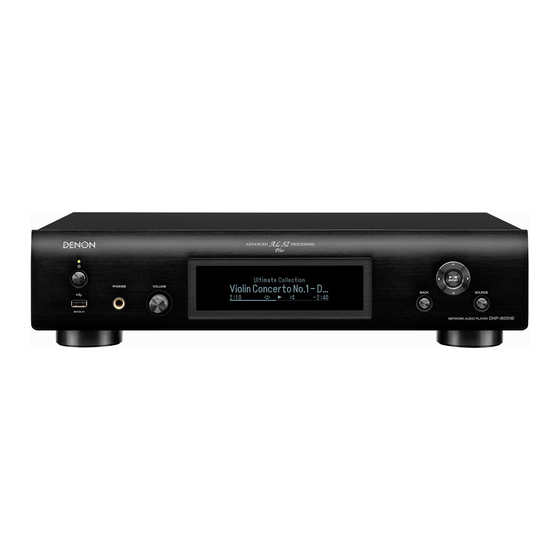
Denon DNP-800NE Service Manual
Network audio player
Hide thumbs
Also See for DNP-800NE:
- Owner's manual (126 pages) ,
- Quick start manual (12 pages) ,
- Owner's manual (115 pages)
Table of Contents
Advertisement
Quick Links
NETWORK AUDIO PLAYER
DNP-800NE
• For purposes of improvement, specifications and design are subject to change without notice.
• Please use this service manual when referring to the operating instructions without fail.
• Some illustrations used in this service manual are slightly different from the actual product.
Service Manual
Click here!
On-line service parts list
http://dmedia.dmglobal.com/Document/DocumentDetails/24926
ONLINE PARTS LIST
(P5)
WEB owner's manual
NA:
http://manuals.denon.com/DNP800NE/NA/EN/index.php
EU:
http://manuals.denon.com/DNP800NE/EU/DE/index.php
JP:
http://manuals.denon.com/DNP800NE/JP/JA/index.php
Upload is planned for the time of a future press release.
BEFORE SERVICING THIS UNIT
ELECTRICAL
MECHANICAL
REPAIR INFORMATION
UPDATING
Please refer to the MODIFICATION NOTICE.
Confidential
Ver. 2
Advertisement
Table of Contents

Related Manuals for Denon DNP-800NE


Summary of Contents for Denon DNP-800NE
- Page 1 Service Manual Ver. 2 NETWORK AUDIO PLAYER DNP-800NE Click here! On-line service parts list http://dmedia.dmglobal.com/Document/DocumentDetails/24926 ONLINE PARTS LIST (P5) WEB owner’s manual http://manuals.denon.com/DNP800NE/NA/EN/index.php http://manuals.denon.com/DNP800NE/EU/DE/index.php http://manuals.denon.com/DNP800NE/JP/JA/index.php Upload is planned for the time of a future press release. BEFORE SERVICING THIS UNIT...
- Page 2 BEFORE SERVICING THIS UNIT SAFETY PRECAUTIONS NOTE FOR SCHEMATIC DIAGRAM HANDLING THE SEMICONDUCTOR AND OPTICS ONLINE PARTS LIST Accessing the Parts List Searching Part Numbers or Ref. Numbers NOTE FOR PARTS LIST SERIAL NUMBER Serial Number Organization SKU Code of this Unit POST-SERVICE PRECAUTIONS Initializing this Unit...
-
Page 3: Safety Precautions
SAFETY PRECAUTIONS The following items should be checked for continued protection of the customer and the service technician. Leakage current check Before returning the set to the customer, be sure to carry out either (1) a leakage current check or (2) a line to chassis resistance check. If the leakage current exceeds 0.5 milliamps, or if the resistance from chas- sis to either side of the power cord is less than 460 kohms, the set is defective. -
Page 4: Note For Schematic Diagram
NOTE FOR SCHEMATIC DIAGRAM WARNING: Parts indicated by the z mark have critical characteristics. Use ONLY replacement parts recommended by the manufacturer. CAUTION: Before returning the set to the customer, be sure to carry out either (1) a leakage current check or (2) a line to chassis resistance check. -
Page 5: Note For Parts List
ONLINE PARTS LIST Accessing the Parts List Searching Part Numbers or Ref. Numbers (1) Access from the Service Manual You can search a Parts List for part numbers or Ref. numbers. ・ Click the URL link on the cover of the service manual. (1) Enter the part number or Ref. - Page 6 SERIAL NUMBER Serial Number Organization The 14-digit serial number that contains the code of the manufacturing plant and the manufacturing date. 14 digits Factory Manufactured Cumulative Year, month code code serial number The last Month 2digit of year (01 ~ 12) SKU Code of this Unit Product SKU SKU Code...
-
Page 7: Initializing This Unit
POST-SERVICE PRECAUTIONS Initializing this Unit Make sure to initialize this unit after replacing the microcomputer or any peripheral equipment, or the PCB. 1. Press the power operation button to turn off the power, and remove the AC plug from the socket. 2. -
Page 8: Schematic Diagrams
ELECTRICAL SCHEMATIC DIAGRAMS SCH01 DIR_PLD SCH02 FPGA SCH03 CPU SCH04 AUDIO SCH05 LEGO SCH06 POWER SCH07 FRONT SCH08 HEADPHONE SCH09 SMPS PRINTED CIRCUIT BOARDS FRONT, HEADPHONE, USB, GUIDE A/B MAIN, SMPS BLOCK DIAGRAM POWER DIAGRAM WIRING DIAGRAM SEMICONDUCTORS 1. IC's 2. - Page 9 SCHEMATIC DIAGRAMS SCH01 DIR_PLD DNP-800NE DIR_PLD TO 0A TO 1A TO 2A FROM FROM CPU BLOCK FROM CPU BLOCK LEGO BLOCK R500 1K-1608 Q500 RT1N141C R501 4K7-1608 C500 100N-K-1608 FROM NET PHY *FILTER COMPONENTS R502 33-1608 R503 0-1608 VALUE TYPE...
- Page 10 SCH02 FPGA DNP-800NE FPGA 33_VCCIO EMPHASIS AL32_TEST4 /INT_EXT FPGA_RES2 FPGA_RES3 FPGA_RES4 FPGA_VER_CONT 33_VCCIO TEST1 DGND AL32_TEST5 MCK_IN DGND 33_VCCIO ASDO_DATA1 AL32_TEST3 33_VCCIO DGND 33_VCCIO DGND 33_VCCIO PCM_DATA/DSD_DATA_R_IN FLASH_NCE_NCSO PCM_BCK/DSD_DBCK_IN 12_VCC DGND DGND 12_VCC PCM_LRCK/DSD_DATA_L_IN R581 0-1608 PLD_DAC1_DATA/DSDR. PCM_DATA/DSD_DATA_R_IN From R582 0-1608 PLD_DAC1_LRCK/DSDL.
- Page 11 SCH03 CPU CP500 TO FRONT B'D DNP-800NE CPU TO CP100 CP500 04-6232-127-008-800+ NET_FACT_RST E_CTS_MIEO E_RTS_MOEI TO 3B E_RXD_MIEO TO LEGO E_TXD_MOEI BLOCK C_PLD_CS. AIOS4_WAKEUP C_PLD_MDI. AIOS4_STBY_STATUS C_PLD_MDO. I2C_SDA TO 4B C_PLD_CLK. I2C_SCL R635 2K2-1608 DGND I2C_SDA R636 2K2-1608 I2C_SCL DIR_DIN C_USBB_MCK_SEL.
- Page 12 SCH04 AUDIO DNP-800NE AUDIO BKT500 BKT501 FG501 FG502 FG500 M3 BRAKET M3 BRAKET FG503 GND PLATE GND PLATE GND PLATE DGND GND PLATE AGND DGND DGND DGND DGND DGND DGND AGND -12V_A R778 47-AX B BLOCK VR_L_IN C680 2N2(EB)-100V R780...
- Page 13 SCH05 LEGO DNP-800NE LEGO FROM CPU BLOCK TO B3 R895 OPEN R896 33-1608 NET_I2S0_DOUT. IN/OUT OUT/IN L503 NFL21SP506XC3 FROM NET3.3V NET3.3V R897 OPEN R898 33-1608 NET5V POWER BLOCK NET_I2S0_BCLKOUT. IN/OUT DGND OUT/IN TO 8C L504 NFL21SP506XC3 R899 OPEN R900 33-1608 NET_I2S0_LRCKOUT.
- Page 14 SCH06 POWER DNP-800NE POWER NET5V D522 LBAS16HT1G TO LEGO BLOCK IC513 BD503 TLV70233-3.3V Q522 CB05YTYH221-2012 TO C8 FDC608PZ NET3.3V BD505 CB05YTYH221-2012 R1077 10K-1608 FROM FROM CPU BLOCK CPU BLOCK NET3V3_POWER TO C6 R1076 R1078 10K-1608 TO C5 0-1608 C835 NET5V_POWER...
- Page 15 SCH07 FRONT DNP-800NE FRONT CP100 FROM MAIN B'D TO CP500 CP100 RMC100 6232-027-102-800 R120 +3.3V_CPU C100 47/16(6.3*5) GND_D REMOTE_ C102 100N-K R121 USB_SW B'D Q120 +16V_OLED RT1P141C REMOTE. C103 R164 10N-K D107 LBAS16HT1G C124 100P-J C104 L101 100N-K CB05YTYH221 Vout...
- Page 16 SCH08 HEADPHONE DNP-800NE HEADPHONE R177 R178 100(1) 100(1) C158 C149 -7V5 R130 Q102 2SA1312 D103 LBAS16HT1G AGND J100 R131 R132 12-AX 12-AX C142 220/25(RFO) R133 JUMPER R134 47-AX R135 47-AX HP_L L102 CB05YTYH221 R138 R145 R136 R137 12-AX 12-AX R139...
- Page 17 SCH09 SMPS T821 T821 CN221 CN221 ER2828(12P) ER2828(12P) D221 D221 L223 L223 20010WS-11 20010WS-11 HS1G HS1G 4.7uH 4.7uH +12V_A +12V_A C805 C805 D801 D801 D802 D802 68uF 68uF R821 R821 C821 C821 R246 R246 + C221 + C221 + C223 + C223 C224 C224...
-
Page 18: Printed Circuit Boards
PRINTED CIRCUIT BOARDS FRONT, HEADPHONE, USB, GUIDE A/B Lead-free Solder When soldering, use the Lead-free Solder (Sn-Ag-Cu). FRONT (A SIDE) FRONT (B SIDE) JP131 (MP) FRONT FRONT (MP) Q115 Q111 7020-08292-000-0S 7020-08292-000-0S JP132 JP154 JP112 1. LED_GREEN CP101 S104 2. LED_RED JP129 3.GND_D JP111... - Page 19 MAIN, SMPS MAIN (A SIDE) MAIN (B SIDE) OPT OUT (GRAY) WHITE WHITE BURRING BURRING BKT500 BKT501 JACK500 JACK501 C621 C623 N501 C650 C638 C728 C637 L502 C651 C655 C620 C624 CP501 C619 C625 C652 C622 C729 C636 TC7WHU04 C539 JACK502 R580 IC500...
-
Page 20: Block Diagram
BLOCK DIAGRAM DNP-800NE AUDIO DIAGRAM 5M570ZF256C5N (PLD) SPDIF OUT1 EP4CE15F17C8N (FPGA) AL32 PROCESSING PCM/DSD DATA/BCK/LRCK PCM/DSD MCK/DATA/BCK/LRCK AUDIO DAC (PCM1795) MCLK I2S-0 I / V AMP I / V AMP RJ-45 RX+/- TX+/- I2S-0 (PCM OUT <= 24bit/192kHz ) LEGO I2S-1 (PCM OUT >... -
Page 21: Power Diagram
POWER DIAGRAM DNP-800NE POWER DIAGRAM SMPS BLOCK +12V_A (OPAMP) IC520 +12V_A KIA7807API +7V_A (NJU72343) Q549 IC509 NJM7805 +5V_A (PCM1795) AGND IC510 +3V3_A (PCM1795) BA033T IC519 -12V_A KIA7907PI -7V_A (NJU72343) Q547 -12V_A (OPAMP) AGND IC100 +16V_OLED +18V_OLED NJM2387ADL3 DGND IC521 +3V3_CPU... -
Page 22: Wiring Diagram
WIRING DIAGRAM DNP-800NE WIRING DIAGRAM VARIABLE OUT FIXED OUT SMPS PCB MAIN PCB OPT OUT RESET RJ-45 RC-5 PCM9211 LEGO NJU72343 PCM1795 UCOM FPGA POWER S/W POWER_RED FRONT PCB H/P PCB POWER_S/W NJM2114M USB PCB (H/P AMP) OLED KEY1-KEY8 MXS-4046A... - Page 23 SEMICONDUCTORS Only major semiconductors are shown, general semiconductors etc. are omitted to list. The semiconductor which described a detailed drawing in a schematic diagram are omitted to list. 1. IC's R5F5631FDDFB (DIGITAL : U503) Port Name I/O STBY MODE Function NORMAL NETWORK 14 VCL...
- Page 24 Port Name I/O STBY MODE Function Port Name I/O STBY MODE Function NORMAL NETWORK NORMAL NETWORK 42 RESERVED P15/RXD1/IRQ5 USBB(XMOS) Control Pin, IRQ5 71 RESERVED OPEN 43 RESERVED P14/IRQ4 USBB(XMOS) Control Pin, IRQ4 72 I O E X P _ I 2 C _ I/O I/O I/O Expander I2C SDA 44 RESERVED...
- Page 25 Port Name I/O STBY MODE Function Port Name I/O STBY MODE Function NORMAL NETWORK NORMAL NETWORK 108 A I O S 4 _ E t h e r n e t ( L E G O ) c o n t r o l p i n f o r 139 KEY1 P41/IRQ9-DS/AN001 Key Control Signal Input Pin (When...
- Page 26 *For adjustable version only. Figure 1. Typical Application Circ Figure 1. Typical Application Circuit PCF8574APWR (MAIN : IC503,U504) NCP380 (MAIN : U509) ILIM* PAD1 ILIM* ILIM* PAD1 FLAG FLAG FLAG Terminal Function TSOP−5 UDFN6 TSOP−6 FLAG FLAG Pin Functions (Top view) TYPE DESCRIPTION NAME...
- Page 27 PCM9211 PCM9211 (MAIN:U502) www.ti.com SBAS495 – JUNE 2010 PIN CONFIGURATIONS DESCRIPTION PT PACKAGE NAME LQFP-48 TOLERANT (TOP VIEW) MS/ADR1 Software control I/F, SPI chip select / I2C slave address setting1(2) MODE Control mode setting, (see the Serial Control Mode section, ERROR/INT0 VDDRX Control Mode Pin Setting)
- Page 28 PCM9211 www.ti.com SBAS495 – JUNE 2010 PCM9211 BLOCK DIAGRAM PCM1795 (MAIN(Audio) : IC508) BLOCK DIAGRAM FILT AUXIN 0 AUTO RXIN7 RXIN 0 RXIN0 SCKO DOUT RXIN 1 RXIN1 MAIN OUTPUT RXIN 2 RXIN2 AUXIN0 LRCK SCKO/ BCK/LRCK PORT RXIN 3 RXIN3 AUXIN1 DOUT...
- Page 29 preventing damaging current backflow through the device when it is powered down. SN74LVC244A GQN OR ZQN PACKAGE OCTAL BUFFER/DRIVER (TOP VIEW) WITH 3-STATE OUTPUTS NJU72343_J (MAIN(Audio) : IC504) SN74LVC244APWR(MAIN:U500、U504) www.ti.com SCAS414X – NOVEMBER 1992 – REVISED MARCH 2005 FEATURES DB, DGV, DW, N, NS, OR PW PACKAGE •...
-
Page 30: Oled Display
2. OLED DISPLAY MXS4035A MXS4035A IO Interfaces... - Page 31 VOLUME ▼ Player (2H) Network Player (4H) Variable VOLUME DOWN (065H) 72H 00000100 00101010 01100000 01001110 Extended Code DNP-800NE must receive following codes. These codes are not included in the RC-1224 KEY No. Key Name Genre 1(D Genre 2(D DATA Code (D...
- Page 32 MECHANICAL DISASSEMBLY Flowchart 1. FRONT PANEL ASSY 2. MAIN PCB 3. SMPS PCB EXPLODED VIEW PACKAGING VIEW...
- Page 33 DISASSEMBLY Flowchart • Remove each part following the flow below. • Reassemble the removed parts in the reverse order. • Read "SAFETY PRECAUTIONS" before reassembling the removed parts. • If wire bundles are removed or moved during adjustment or part replacement, reshape the wires after completing the work. Failure to shape the wires correctly may cause problems such as noise. • See "EXPLODED VIEW" TOP COVER FRONT PANEL ASSY MAIN PCB SMPS PCB DISASSEMBLY DISASSEMBLY DISASSEMBLY 2. MAIN PCB 1. FRONT PANEL ASSY 3. SMPS PCB and "EXPLODED VIEW" and "EXPLODED VIEW" and "EXPLODED VIEW" FRONT PCB MAIN PCB SMPS PCB Ref. No. of EXPLODED VIEW : P 3 Ref. No. of EXPLODED VIEW : P 8 Ref. No. of EXPLODED VIEW : P 5 LEGO PCB USB PCB Ref. No. of EXPLODED VIEW : P 7 Ref. No. of EXPLODED VIEW : P 1 H/P PCB Ref. No. of EXPLODED VIEW : P 2...
-
Page 34: Front Panel Assy
1. FRONT PANEL ASSY • For the shooting direction of each photos used in this manual, see the photo below. • A, B, C and D in the photo below indicate the shooting directions of photos. Proceeding : TOP COVER → FRONT PANEL ASSY • The photographs with no shooting direction indicated were taken from the top of the unit. (1) Remove the screws. Remove the Volume knob. Remove the Washer. • Photos of DNP-800NE BKE2 are used in this manual. The viewpoint of each photograph (Shooting direction : X) [View from the top] ↓Shooting direction: B↓ Washer View from the bottom Remove the connector wire, FFC and screws. CP500 Loosen ↑Shooting direction: A↑... - Page 35 2. MAIN PCB 3. SMPS PCB Proceeding : TOP COVER → MAIN PCB Proceeding : TOP COVER → SMPS PCB (1) Remove the screws. See "EXPLODED VIEW" for instructions on removing the SMPS PCB. Remove the connector wire, FFC and screws. CP500 STYLE PIN CN500 CP503 CN221 Antenna connector (3) LEGO PCB Proceeding : TOP COVER LEGO PCB →...
-
Page 36: Exploded View
EXPLODED VIEW http://dmedia.dmglobal.com/Document/DocumentDetails/24926 Parts List : (Top cover inside) S7X2 S6X5 21 X4 S7X2 S8X4 S11X1 S4X4 S6X7 S5X4 S8X5 S9X2 S1X2 S1X4 S8X1 S8X1 S5X4 26X2 S2X1 S3X3 S1x4 S1X1 S1X9 15X2 16 X4 S10X4 17 X4 WARNING: z 印の部分は安全を維持するために重要な部品です。 従って交換時は必ず指定の部品を使用してください。... - Page 37 PACKAGING VIEW http://dmedia.dmglobal.com/Document/DocumentDetails/24926 Parts List : 22) Manual Assy 22-7)Poly Bag 22-1)SPOTIFY Insertion sheet SHEET 22-2)Safety instruction 22-3)Caution on Using Batteries(E2 only) 22-4)Warrnty card(E3 only) 22-5)Instruction Manual 22-6)Quick Manual SHEET Antenna *2 22-8)Note on Radio Sheet 10 X2 S E T F R O S E T S E T...
-
Page 38: Repair Information
REPAIR INFORMATION TROUBLE SHOOTING 1. POWER 2. OLED 3. No Remote Control Reception 4. Audio is not output due to a problem in the analog circuit (Line Out, Variable Out, H/P Out) 5. Audio is not output during USB file playback, server file playback, internet radio or Bluetooth playback due to a problem in the digital circuit 6. - Page 39 TROUBLE SHOOTING 1. POWER 1.1. The unit does not power on Check that the LED is lit (when connected to the Check the Protection history. Can the "Protection History" be checked? AC inlet). [DC PROTECTION1] Does the POWER indicator blink in red immedi- ("1-3.
- Page 40 1.3. Power Supply Voltage Abnormalities Check the voltage level (when the POWER switch is turned on) Replace any faulty parts. [CN221: 11pin] Or replace the SMPS PCB. Check the output voltage. SMPS PCB to MAIN PCB "Hi" : 3.3V, "Lo": 0V? [CN221 : 1pin] = +12V ±...
- Page 41 2. OLED 2.1. OLED is not lit Checking the Digital communication waveform. Check that the connection is correct and recon- (after starting the power supply)。 The SYSTEM uCOM is malfunctioning or latched. Check the cable and its connection. nect FFC. FRONT PCB [CP100 : 3-14pin] Check each part listed after "1.4.
- Page 42 3. No Remote Control Reception Check that you are using a [RC-1224] remote control and replace the batteries. Can a square wave be found? MCU[U503 : 26pin] is faulty. Point the remote control at the unit and check . Replace the MCU[U503]. MAIN PCB : [CP500 : 11pin] Or replace the MAIN PCB.
- Page 43 4. Audio is not output due to a problem in the analog circuit (Line Out, Variable Out, H/P Out) This section details items to check if the digital audio signal is being correctly input to the MAIN PCB DAC IC [IC508]. Check the Clock.
- Page 44 Check the audio signal. Check the output signal. There may be an abnormality in the combined differential at a Set "Variable Out" and "Phones" to ON in "Audio" in the menu MAIN PCB point after the I/V conversion circuit. settings. Are signals output from all of the I/V converter circuit outputs (4 Refer to the circuit diagram and check for open parts or a short Line Out, Variable Out, H / P Out output terminal.
- Page 45 5. Audio is not output during USB file playback, server file playback, internet radio or Bluetooth playback due to a problem in the digital circuit Before testing circuit operation, check if the file to be played back is in a supported format and network settings are correct. There is a malfunction in the communication between the following areas or in LEGO Module.
- Page 46 6. Audio is not output from OPT OUT Check the following areas to identify the area where the S/PDIF Check the S/PDIF signal. signal is cut off. MAIN PCB Malfunctions in the OPT INPUT terminal, DIR[U502] : [R580]OPT OUT power supply voltage [5V] of Output buffer IC[IC500], input/output Check input of digital audio waveform during playback of OPT OUT.
- Page 47 MEASURING METHOD AND WAVEFORMS 1. MAIN PCB test point Check playback from the applicable input source. (It is recommended to use extension wires between the probe and test points.) OPT OUT (GRAY) WHITE BURRING WHITE BURRING MAIN PCB : test point BKT500 JACK500 JACK501...
- Page 48 WAVEFORMS 1-3 DAC input PCM BCK_LRCK_DATA 4-6 Network playback PCM BCK_LRCK_DATA q PCM r NET_PLD_I2S0_BCK w PCM_WCK t NET_PLD_I2S0_LRCK e PCMDATA y NET_PLD_I2S0_DATA 7-10 DAC input PCM_BCK_LRCK_DATA 11-13 DIT input PCM_BCK_LRCK_DATA Q1 PLD_DTI_PBCK u PCM_BCK i WCK_DSDR Q2 PLD_DTI_LRCK o PCM_DATA_L Q3 PLD_DTI_DATA Q0 PCM_DATA_R...
-
Page 49: Special Mode Setting Button
SPECIAL MODE Special mode setting button b No. 1: Insert the AC plug while pressing button "A", and wait for more than 3 seconds. b No. 2 - 4: Insert the AC plug while pressing buttons "A" and "B" together, and wait for more than 3 seconds. b No. - Page 50 1. Selecting the Mode1 for Service-related 1.1. Actions Selecting Each Mode. 1.2. Starting up Insert the AC plug while pressing button "POWER", and wait for more than 3 seconds. Release button "POWER" when the power indicator turns green. Executes an update for the entire device via DPMS. Select the desired mode using the "CURSOR f / d "...
-
Page 51: Version Display Mode
o HEOS Locate 1-1. Version Display Mode 1-1.1. Actions Version information is displayed when the device is started in this mode. 1-1.2. Starting up Q0 HEOS Restore Insert the AC plug while pressing button "POWER", and wait for more than 3 seconds. Release button "POWER"... -
Page 52: Protection History Display Mode
• Display when protection has been activated 1-2. IR Control Test This function is used to check IR control operations. 1-2.1. Starting up Insert the AC plug while pressing button "POWER", and wait for more than 3 seconds. Cause : Power supply short circuit detected in the power supply board Release button "POWER"... - Page 53 1-5. Initialize Initializes all MCU and network module backup data. NOTE: If initialization is executed in LEGO Off mode, cancel LEGO off mode then reset the LEGO Net- work. 1-5.1. Starting up Insert the AC plug while pressing button "POWER", and wait for more than 3 seconds. Release button "POWER"...
- Page 54 2. Factory Initialization Mode 4. Firmware Factory Restore Used when replacing the Network module. Initialize backup data of the MCU. "3. Update method when the MAIN PCB or network module is replaced (Using a USB flash drive U503, U502, U501, NETWORK MODULE)"...
- Page 55 (3) When saving of the log package fails, "USB Failed" appears in the display for 5 seconds, regardless of 6. Selecting the Mode2 for Service-related whether the upload to the server was successful. Selecting Each Mode. 6.1. Starting up While the power is on, hold down buttons "POWER" and "ENTER" for at least 3 seconds. (1) "LEGO Log Capture Mode"...
- Page 56 UPDATING PROCEDURE AFTER REPLACING THE PCB. PROCEDURE AFTER REPLACING THE U-COM, ETC. FIRMWARE UPDATE PROCEDURE 1. Items necessary for update 2. Update preparation with a USB flash drive (U503, U502, U501, NETWORK MODULE) 3. Update method when the MAIN PCB or network module is replaced (Using a USB flash drive U503, U502, U501, NETWORK MODULE) 4.
- Page 57 PROCEDURE AFTER REPLACING THE PCB. PROCEDURE AFTER REPLACING THE U-COM, ETC. The procedure after replacing the printed circuit boards is as follows. The procedure after replacing the u-COM (microprocessor) is as follows. (1) Change the resistor for setting the region. Implement the update method when the MAIN PCB or network module is replaced.
-
Page 58: Firmware Update Procedure
Update download file when the firmware is updated (Two files, "HW component" and "LEGO component") Download from SDI Model Name Model Area For HW component For LEGO component DNP-800NE E3 North America (E3) Product ID : 000200190100 DNP-800NE E2 Europe (E2) Product ID : 000200190200 DPMS_DNP800NEALL_LEGO_xxx.zip... - Page 59 2. Update preparation with a USB flash drive (U503, U502, U501, NETWORK MODULE) You can update the firmware by downloading the latest version with USB flash drive. 2.1. Connecting to the USB flash drive (1) Preparation • Windows PC • USB flash drive format : Prepare a USB flash drive formatted in FAT16 or FAT32. b We recommend a USB flash drive that has an LED installed.
-
Page 60: Start The Update
3. Update method when the MAIN PCB or network module is replaced (Using a USB flash drive U503, U502, U501, NETWORK MODULE) 3.1. File structure on USB flash drive (5) USB Update starts automatically. The Standby LED lights red. MAIN PCB or network module is replaced onto the USB flash drive in the following structure. Display during USB update After unzipping the files, store them in the root of the same USB flash drive. - Page 61 NOTE : Enter the file name in double quotation marks. (The file extension is not required.) (English is selected) (Japanese is selected) Service Region File name (4) Insert the USB flash drive into the USB port. North America "denon-config-locale-set-1" Europe "denon-config-locale-set-2" Japan "denon-config-locale-set-3" Download firmware Australia "denon-config-locale-set-4"...
- Page 62 5. Normal Firmware Update Method from USB Flash Drive (U503, U502, U501, NETWORK MODULE) 5.1. File structure on USB flash drive (1) Press the power button to turn on the power. (2) Wait for this unit to start up. Copy the normal update files onto the USB flash drive in the following structure. (3) Set the input source to Internet Radio.
-
Page 63: Network Connection
6. Normal Firmware Update Method from OTA (U503, U502, U501, NETWORK MODULE) 6.2. Check and update the firmware Download the latest firmware from our website and update the firmware. Check if there is a firmware update available. It is also possible to check approximately how long the ---Cautions on Firmware Update--- update will take. - Page 64 7. About the error codes (U503, U502, U501, NETWORK MODULE) See the table below for details on error codes and solutions when updating the firmware. Device ID table Error codes are displayed in 4 digits, : DeviceID, : ErrorCode). YYXX Device ID ( YY ) Device Name Display...
- Page 65 Copyright © 2018 D&M Holdings Inc. All Rights Reserved.
Need help?
Do you have a question about the DNP-800NE and is the answer not in the manual?
Questions and answers