Sony XVM-R75 Service Manual
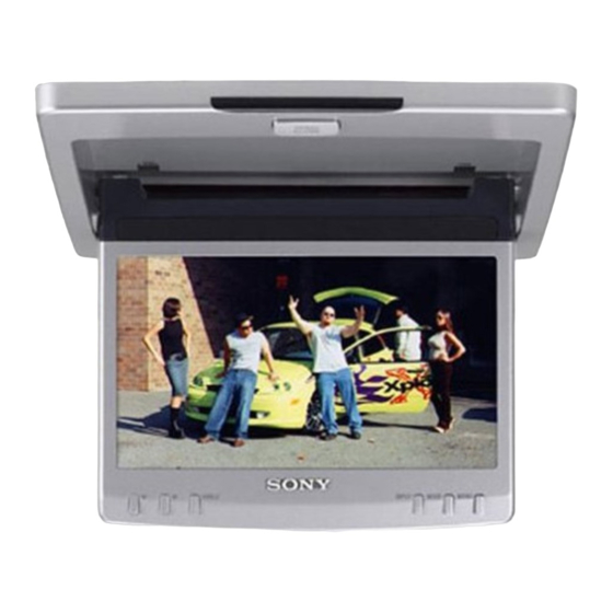
Overhead monitor
Hide thumbs
Also See for XVM-R75:
- Operating instructions manual (64 pages) ,
- Operating instructions manual (104 pages) ,
- Training manual (62 pages)
Table of Contents
Advertisement
Quick Links
SERVICE MANUAL
Ver 1.1 2002. 08
•
This set consists of the following units.
MONITOR
XVM-R75
CONNECTION BOX
XA-117
REMOTE COMMANDER
RM-X123
Monitor
System
Liquid crystal color display
Display
Motorized flipdown panel
Drive system
TFT-LCD active matrix
system
Picture size
7 inches wide screen (16:9)
154 × 87 mm, 176 mm
× 3
(6
in., 7 in.)
1/8
1/2
(w/h, d)
Picture segment
336,960 (w 1440 × h 234) dots
Power requirements
12 V DC car battery
(negative ground)
Current drain
Approx. 1.5 A
Dimensions
US, Canadian model:
202 × 45 × 243 mm
(8 × 1
× 9
in.)
13/16
5/8
(w/h/d)
EXCEPT US, Canadian model:
230 × 50 × 270 mm
(w/h/d)
Operating temperature
5 °C – 45 °C
(41 °F – 113 °F)
Mass
US, Canadian model:
Approx. 1.2 Kg (2 lb 10 oz)
EXCEPT US, Canadian model:
Approx. 1.3 Kg
Sony Corporation
9-874-115-02
2002H0400-1
e Vehicle Company
© 2002. 08
Published by Sony Engineering Corporation
XVM-R75
SPECIFICATIONS
Connection box XA-117
A/V Output
Output Impedance: less than 220 Ω
Output Level:
Video:
A/V Input × 3
Input Impedance:
Input Level:
Video:
DC output
Dimensions
Mass
US Model
Canadian Model
AEP Model
UK Model
E Model
less than 100 pF
0 dBs ±0.3 dB
(0.775 V rms)
(Vol Max)
75 Ω 1Vp-p
more than 10 K Ω
less than 1000 pF
0 dBs ± 0.3 dB
(0.775 V rms)
75 Ω 1 Vp-p
7.5 V (max 2 A)
101 × 42 × 73 mm
(4 × 1
× 2
in.)
11/16
7/8
(w/h/d)
Approx. 150 g (5 oz)
– Continued on next page –
OVERHEAD MONITOR
1
Advertisement
Chapters
Table of Contents

Related Manuals for Sony XVM-R75


Summary of Contents for Sony XVM-R75
- Page 1 (41 °F – 113 °F) Mass US, Canadian model: Approx. 1.2 Kg (2 lb 10 oz) EXCEPT US, Canadian model: Approx. 1.3 Kg OVERHEAD MONITOR Sony Corporation 9-874-115-02 2002H0400-1 e Vehicle Company © 2002. 08 Published by Sony Engineering Corporation...
-
Page 2: Table Of Contents
REPLACE THESE COMPONENTS WITH SONY PARTS WHOSE NE REMPLACER CES COMPOSANTS QUE PAR DES PIÈCES PART NUMBERS APPEAR AS SHOWN IN THIS MANUAL OR SONY DONT LES NUMÉROS SONT DONNÉS DANS CE MANUEL IN SUPPLEMENTS PUBLISHED BY SONY. OU DANS LES SUPPLÉMENTS PUBLIÉS PAR SONY. -
Page 3: Location Of Controls
XVM-R75 SECTION 1 GENERAL This section is extracted from instruction manual. Location of Controls Monitor 1 Receptor for the card remote 5 MODE button 10 commander Press to change the screen mode. 2 OPEN/CLOSE button 9 6 INPUT button 11 Press to open and close the monitor. - Page 4 XVM-R75 Card remote commander RM-X123 9 ATT button 14 qs POWER button 9 Press to quickly attenuate the qd MENU button 12, 13 volume. Press to adjust the various display 0 MODE button 10 settings. Press to change the screen mode.
-
Page 5: Connection Diagram
XVM-R75 Connection diagram Refer to the connection diagram for the proper connections. You can make connections shown in A area. Please ask a qualified technician for the other connections. Master unit (optional) To Speakers/Amplifier/Subwoofer (optional) To AUX IN 0.1 m... - Page 6 XVM-R75 Power supply cord GND (1 m) cramper (Black) (supplied) Note To a metal surface After connecting, bundle up the of the car chassis GND (1 m) connecting cords by attaching (Black) the supplied cramper. Back-up (5 m) (Yellow) Audio L/R/Video Input...
-
Page 7: Disassembly
XVM-R75 SECTION 2 DISASSEMBLY Note : This set can be disassemble according to the following sequence. 2-1. LCD BLOCK ASSY 2-2. CONNECTORS (Page 7) (Page 8) 2-3. MAIN BOARD (Page 8) 2-4. MOTOR (M1), 2-5. DISPLAY BOARD MICRO SW BOARD... -
Page 8: Connectors
XVM-R75 2-2. CONNECTORS 4 connector 6 connector 8 connector (B10) (B9) 3 connector (B1) 5 connector (B8) 7 connector (B2) 9 connector (B12) (B5) 0 connector 2 connector (B13) (B11) 1 connector (B7) 2-3. MAIN BOARD 2 P 2.6x6 1 P 2.6x6... -
Page 9: Motor (M1), Micro Sw Board
XVM-R75 2-4. MOTOR (M1), MICRO SW BOARD 2 K 2x3 3 metal cover 1 K 2x3 5 motor (M1) 4 P 2.6x3.5 6 P 2x2.5 7 MICRO SW board 2-5. DISPLAY BOARD 4 K 2x5 5 bottom cover 9 P 2x5... -
Page 10: Diagrams
XVM-R75 SECTION 3 DIAGRAMS • Waveforms (MAIN Board) • Waveforms (DISPLAY Board) 2V/DIV 20µsec/DIV 0.5V/DIV 20µsec/DIV 2V/DIV 1µsec/DIV 4.0Vp-p 1.0Vp-p 5.6Vp-p 2.25µsec (B_OUT) U600 (VIN2) 0.2V/DIV 20µsec/DIV 1V/DIV 20µsec/DIV 10V/DIV 5µsec/DIV 0.7Vp-p 2.0Vp-p 20Vp-p 19.5µsec (VOUT) (SYN_S) U600 5V/DIV 20µsec/DIV 1V/DIV 0.2µsec/DIV... -
Page 11: Circuit Boards Location
• B : B– Line. • H : adjustment for repair. MAIN board • B13 of XVM-R75 is connected to Connection Box with a monitor cable. Power voltage is dc 14.4 V from ACC cord of the Connec- tion Box and fed with regulated dc power supply. - Page 12 XVM-R75 3-2. PRINTED WIRING BOARD — MAIN SECTION (1/2) — • Refer to page 11 for Circuit Boards Location and Common Note on Printed Wiring Boards. MAIN BOARD (COMPONENT SIDE) • Semiconductor Location Ref. No. Location F-10 E-12 H-10 G-10...
- Page 13 XVM-R75 3-3. PRINTED WIRING BOARDS — MAIN SECTION (2/2) — • Refer to page 11 for Circuit Boards Location and Common Note on Printed Wiring Boards. E-PHONE BOARD MAIN BOARD (CONDUCTOR SIDE) (COMPONENT SIDE) CONTROL OUTPUT (IR) AUDIO L R105...
-
Page 14: Schematic Diagram -Main Section (1/2)
XVM-R75 Ver 1.1 3-4. SCHEMATIC DIAGRAM — MAIN SECTION (1/2) — • Refer to page 10 for Waveforms and page 11 for Common Note on Schematic Diagram. R128 R112 R126 IC B/D R129 C5 R6 R111 R127 R63 R62 R132... - Page 15 XVM-R75 Ver 1.1 3-5. SCHEMATIC DIAGRAM — MAIN SECTION (2/2) — • Refer to page 10 for Waveforms and page 11 for Common Note on Schematic Diagram. (Page 14) R104 R546 R525 R530 R508 R561 R509 C511 R572 C510 U505...
-
Page 16: Printed Wiring Board -Display Section (1/2)
XVM-R75 3-6. PRINTED WIRING BOARD — DISPLAY SECTION (1/2) — • Refer to page 11 for Circuit Boards Location and Common Note on Printed Wiring Boards. DISPLAY BOARD (COMPONENT SIDE) DOWN MENU DIMMER MODE INPUT 9-885-025-... -
Page 17: Printed Wiring Board -Display Section (2/2)
XVM-R75 3-7. PRINTED WIRING BOARD — DISPLAY SECTION (2/2) — • Refer to page 11 for Circuit Boards Location and Common Note on Printed Wiring Boards. (Page 13) T0 MAIN BOARD LCD1 DISPLAY BOARD (CONDUCTOR SIDE) LIQUID CRYSTAL DISPLAY PANEL •... -
Page 18: Schematic Diagram -Display Section (1/3)
XVM-R75 Ver 1.1 3-8. SCHEMATIC DIAGRAM — DISPLAY SECTION (1/3) — • Refer to page 10 for Waveforms and page 11 for Common Note on Schematic Diagram. (Page 19) C152 (Page 19) R204 R205 C151 C154 R206 (Page 20) R193... -
Page 19: Schematic Diagram -Display Section (2/3)
XVM-R75 Ver 1.1 3-9. SCHEMATIC DIAGRAM — DISPLAY SECTION (2/3) — • Refer to page 10 for Waveforms and page 11 for Common Note on Schematic Diagram. R447 D410 R446 R445 R652 IC B/D Q603 C419 R448 R503 R501 R502... -
Page 20: Schematic Diagram -Display Section (3/3)
XVM-R75 Ver 1.1 3-10. SCHEMATIC DIAGRAM — DISPLAY SECTION (3/3) — • Refer to page 10 for Waveforms and page 11 for Common Note on Schematic Diagram. L701 R722 R726 R733 L703 R720 C722 R723 R716 U704 C723 ZD701 VFRER... -
Page 21: Exploded Views
XVM-R75 SECTION 4 EXPLODED VIEWS NOTE: • The mechanical parts with no reference • Color Indication of Appearance Parts The components identified by mark 0 or dotted line with mark number in the exploded views are not supplied. Example : 0 are critical for safety. -
Page 22: Cover Section-2
XVM-R75 4-2. COVER SECTION-2 not supplied (OPEN SW board) not supplied not supplied not supplied (POWER SW (E-PHONE board) board) Ref. No. Part No. Description Remark Ref. No. Part No. Description Remark 9-885-025-13 MAIN BOARD, COMPLETE 9-885-025-51 BUTTON (POWER) 9-885-025-36 PLATE, SHIELD... -
Page 23: Lcd Section
9-885-025-60 WIRE, EARTH (L=50mm) 9-885-025-53 BUTTON (R) 9-885-025-44 SHEET 9-885-025-52 BUTTON (L) LCD1 9-885-025-20 DISPLAY PANEL, LIQUID CRYSTAL (TFT) 4-969-961-11 EMBLEM, SONY (7in. WIDE) 9-885-025-55 COVER (IR LED) 9-885-026-24 MOTOR (OPEN/CLOSE) 9-885-025-48 COVER (MONITOR), TOP 7-685-103-29 SCREW, TAPPING +P 2X5... -
Page 24: Electrical Parts List
XVM-R75 SECTION 5 DISPLAY ELECTRICAL PARTS LIST NOTE: • Due to standardization, replacements in • Items marked “*” are not stocked since The components identified by mark 0 or dotted line with mark the parts list may be different from the they are seldom required for routine service. - Page 25 XVM-R75 DISPLAY Ref. No. Part No. Description Remark Ref. No. Part No. Description Remark C611 1-162-969-11 CERAMIC CHIP 0.0068uF 10% C727 1-162-928-11 CERAMIC CHIP 120PF C612 9-885-026-94 CERAMIC CHIP 3.3uF C728 1-107-826-11 CERAMIC CHIP 0.1uF C613 1-162-970-21 CERAMIC CHIP 0.01uF...
- Page 26 XVM-R75 DISPLAY Ref. No. Part No. Description Remark Ref. No. Part No. Description Remark G_DC1 1-216-864-11 METAL CHIP 1/10W Q301 8-729-421-15 TRANSISTOR 2SD1119-Q G_DC2 1-216-864-11 METAL CHIP 1/10W Q501 8-729-901-00 TRANSISTOR DTC124EKA G_DC3 1-216-864-11 METAL CHIP 1/10W Q502 8-729-901-00 TRANSISTOR DTC124EKA...
- Page 27 XVM-R75 DISPLAY Ref. No. Part No. Description Remark Ref. No. Part No. Description Remark R118 1-216-816-11 METAL CHIP 1/10W R502 1-216-821-11 METAL CHIP 1/10W R119 1-216-817-11 METAL CHIP 1/10W R503 1-216-833-11 METAL CHIP 1/10W R120 1-216-821-11 METAL CHIP 1/10W R504...
- Page 28 XVM-R75 DISPLAY Ref. No. Part No. Description Remark Ref. No. Part No. Description Remark R647 1-216-821-11 METAL CHIP 1/10W R746 1-216-809-11 METAL CHIP 1/10W R648 1-216-821-11 METAL CHIP 1/10W R751 1-216-837-11 METAL CHIP 1/10W R649 1-216-821-11 METAL CHIP 1/10W R752...
- Page 29 XVM-R75 DISPLAY E-PHONE MAIN Ref. No. Part No. Description Remark Ref. No. Part No. Description Remark W710 1-216-864-11 METAL CHIP 1/10W 1-135-960-11 CERAMIC CHIP 10uF W713 1-218-271-11 METAL CHIP 1/10W 1-162-927-11 CERAMIC CHIP 100PF W714 1-216-821-11 METAL CHIP 1/10W 1-162-927-11 CERAMIC CHIP...
- Page 30 XVM-R75 MAIN Ref. No. Part No. Description Remark Ref. No. Part No. Description Remark 1-117-681-11 ELECT 100uF 1-216-845-11 METAL CHIP 100K 1/10W 1-107-826-11 CERAMIC CHIP 0.1uF 1-218-285-11 METAL CHIP 1/10W 1-135-960-11 CERAMIC CHIP 10uF 1-216-832-11 METAL CHIP 8.2K 1/10W 1-117-681-11 ELECT...
- Page 31 XVM-R75 MAIN MICRO SW OPEN SW POWER SW Ref. No. Part No. Description Remark Ref. No. Part No. Description Remark 1-216-841-11 METAL CHIP 1/10W 8-759-914-05 IC BA4558F-T1 1-216-841-11 METAL CHIP 1/10W 8-759-345-28 IC ST24C02FM6TR 1-216-841-11 METAL CHIP 1/10W 8-759-710-62 IC NJM2246M...
- Page 32 XVM-R75 POWER SW Ref. No. Part No. Description Remark < IC > IR10 8-748-030-06 INFRARED SBX8030-F < TRANSISTOR > 9-885-026-54 TRANSISTOR BC848B < RESISTOR > 1-216-864-11 METAL CHIP 1/10W 1-216-809-11 METAL CHIP 1/10W 1-216-829-11 METAL CHIP 4.7K 1/10W 1-216-837-11 METAL CHIP 1/10W <...
- Page 33 XVM-R75 US Model Canadian Model SERVICE MANUAL AEP Model UK Model E Model Ver 1.1 2002. 08 SUPPLEMENT-1 File this supplement with the service manual. Subject : Addition of Electrical Adjustments. Addition of Block Diagrams. Addition of IC Block Diagrams.
-
Page 34: Equipment Used
XVM-R75 When measuring, the ground should be connected to the ground (pin 15 of connector B1) in the display board unless otherwise specified. 1-1. EQUIPMENT USED The following measuring equipment are used for these electrical adjustments: • Oscilloscope • NTSC pattern generator •... -
Page 35: Brightness Temporary Level Adjustment
XVM-R75 1-6. BRIGHTNESS TEMPORARY LEVEL 1-14. RGB GAIN (2) ADJUSTMENT ADJUSTMENT 1. Display 5-step gray scale on the monitor screen. 2. Connect oscilloscope to pin wa of IC U600. 1. Display gray scale on the monitor screen. 3. Adjust the semi-fixed resistor VRGB so that the level of the signal 2. -
Page 36: Vcom Bias Adjustment
XVM-R75 1-17. VCOM BIAS ADJUSTMENT 1-18. BLANK LEVEL ADJUSTMENT 1. Display gray scale on the monitor screen. 1. Display gray scale on the monitor screen. Set the screen to the 2. Connect oscilloscope to the Q15 No. 2. Normal mode. -
Page 37: Block Diagram -Main Section
XVM-R75 2-1. BLOCK DIAGRAM — MAIN SECTION — LINE IN SELECT LINE AMP VIV2 AUDIO L VOUT VIN1 VOUT1 AUDIO L (WHITE) VIN1 (WHITE) AUDIO AUDIO R R-CH AUDIO R VIDEO R-CH (RED) (RED) INPUT-I LOGIC AL IN (DVD) VIDEO... -
Page 38: Block Diagram -B/L (Display) Section
XVM-R75 2-2. BLOCK DIAGRAM — B/L (DISPLAY) SECTION — SWITCHNG +11V REG SWITCHNG BATT Q1,3 Q38,39 BACK LIGHT SWITCHNG SYSTEM CONTROL U505 (2/4) FT ON SW Q40,41 TFT ON RD3/PSP3 BACK LIGHT CONTROL FLIP FLOP DIMMER RC2/CCP1 KEY0 KEY MATRIX... -
Page 39: Block Diagram -Rgb (Display) Section
XVM-R75 2-3. BLOCK DIAGRAM — RGB (DISPLAY) SECTION — CHARACTER GENERATOR RGB DECODER U503 U600 B13 (2/2) SYNC SWITCH MEMORY CONT U601 Q501 SCLK XSCK R IN GAMMA AUDIO Q502 VIDEO COMMAND ADDRESS VRAM G IN OSDCS INPUT-2,3 INPUT CONT... -
Page 40: Block Diagram -Lcd (Display) Section
XVM-R75 2-4. BLOCK DIAGRAM — LCD (DISPLAY) SECTION — DISPLAY CONTROL U505 (4/4) U705 ZOOM ZOOM RC5/SDO SIDE1 RE1/AN6 SIDE1 PC7/RX/DT EQUIVALENT PHASE SYNC SYNC VFRER PULSE DELETE COMPARATOR U704 SEPA VCOM SYNC (DISPLAY) (Page 7) COM FRP CSYNC DETECT... -
Page 41: Ic Block Diagrams
XVM-R75 2-5. IC BLOCK DIAGRAMS U1 PT2257-S (MAIN Board) (1/2) U8 BA6247FP-Y (MAIN Board) (2/2) VIN2 VOUT2 CLOCK VR 2 VOL AMP 2 VREF LOGIC CONTROL OUT2 VOL AMP 1 REF AMP OUT3 VR 1 OUT1 VIN1 VOUT1 DATA VCC2... - Page 42 XVM-R75 U505 PIC16C77-04/L (MAIN Board) (2/2) 28 27 26 25 24 23 22 21 20 19 18 DATA BUS PORT A PROGRAM COUNTER EPROM PROGRAM MEMORY 8 LEVEL STACK FILE 2K x 14 (13-BIT) REGISTERS 128 x 8 PROGRAM RAM ADDRESS...
- Page 43 XVM-R75 U600 IR3Y29B4 (DISPLAY Board) (2/3) 24 23 22 18 17 B DC DET SYNC GAMMA 2 GAMMA 0 RGB AMPLITUDE ADJUST CHROMA OUT ACC FILTER KILLER FILTER BRIGHT SUB BRIGHT B SUB BRIGHT R INT/EXT SW R-Y G-Y B-Y...
- Page 44 XVM-R75 U502 M66242FP (DISPLAY Board) (2/3) 8-BIT CONTROL PWM CIRCUIT CIRCUIT 12-BIT PWM1 REGISTER PWM CIRCUIT LOWER BYTE PWM2 REGISTER 4-BIT-RATE MULTIPLIER PWM3 PWM4 XOUT OSCILLATION UPPER BYTE INPUT DIVIDER CIRCUIT REGISTER REGISTER SCLK TO OTHER CHANNELS U503 MB90097 (DISPLAY Board) (2/3)
- Page 45 XVM-R75 U1, 601 74HC4053D (DISPLAY Board) (2/3) 16 VCC LOGIC DECODER LEVEL CONVERSION LOGIC DECODER LEVEL CONVERSION LOGIC DECODER LEVEL CONVERSION U3 TL1451ACPWR (DISPLAY Board) (3/3) REFERENCE VOLTAGE ERROR AMP VREF – +25V – VREF SHORT OUTPUT1 COMP CIRCUIT PROTECTION...
- Page 46 XVM-R75 U4 TC4W53F (DISPLAY Board) (3/3) OUT IN COMMON OUT IN U705 TC203G04AF-0011 (DISPLAY Board) (3/3) RESET RESET SYNCOUT SYNCHRO MODE CIRCUIT VPOS2 SEPARATE CIRCUIT SETTING VDMODE HDDIN CIRCUIT VPOS3 INTEXT MODE SETTING VDIN UONS EQUIVALENT PULSE DELETE CIRCUIT VDOUT...
- Page 47 XVM-R75 MEMO...
- Page 48 XVM-R75 REVISION HISTORY Clicking the version allows you to jump to the revised page. Also, clicking the version at the upper on the revised page allows you to jump to the next revised page. Ver. Date Description of Revision 2002. 06 Addition of Electrical Adjustments, Block Diagrams and IC Block 2002.
Need help?
Do you have a question about the XVM-R75 and is the answer not in the manual?
Questions and answers