Sony XVM-B62 Service Manual
Mobile monitor
Hide thumbs
Also See for XVM-B62:
- Operating instructions manual (28 pages) ,
- Operating instructions manual (15 pages) ,
- Operating instructions manual (40 pages)
Table of Contents
Advertisement
Quick Links
SERVICE MANUAL
Ver. 1.0 2006.02
Sony Corporation
9-887-112-01
eVehicle Division
2006B04-1
Published by Sony Techno Create Corporation
© 2006.02
SPECIFICATIONS
Monitor
System
Liquid crystal color display
Drive system
TFT-LCD active matrix system
Picture size
6.2 inches wide screen (16:9)
137.5 × 77.2 mm
(5
× 3
in.) (w × h)
1/2
1/8
Picture segment
336,960 (w 1440 × h 234) dots
Power requirements
12 V DC car battery (negative ground)
Current drain Approx. 550 mA
Dimensions
164.2 × 106.6 × 29 mm
× 4
× 1
(6
1/2
1/4
1/16
Operating temperature
0 °C – 45 °C (32 °F – 113 °F)
Mass
Approx. 450 g (1 lb)
Supplied accessories
Power supply cord (1)
Video in cable (3 m) (1)
Tap (1)
Collar (1)
Operating Instructions (1)
Monitor stand (1)
(with suppled screws (5))
(E model)
Design and specifications are subject to change
without notice.
XVM-B62
Canadian Model
in.) (w/h/d)
MOBILE MONITOR
US Model
E Model
Advertisement
Table of Contents

Related Manuals for Sony XVM-B62


Summary of Contents for Sony XVM-B62
-
Page 1: Service Manual
Tap (1) Collar (1) Operating Instructions (1) Monitor stand (1) (with suppled screws (5)) (E model) Design and specifications are subject to change without notice. MOBILE MONITOR Sony Corporation 9-887-112-01 eVehicle Division 2006B04-1 Published by Sony Techno Create Corporation © 2006.02... -
Page 2: Table Of Contents
LES COMPOSANTS IDENTIFIÉS PAR UNE MARQUE 0 SUR LES DIAGRAMMES SCHÉMATIQUES ET LA LISTE DES PIÈCES SONT CRITIQUES POUR LA SÉCURITÉ DE FONCTIONNEMENT. NE REMPLACER CES COMPOSANTS QUE PAR DES PIÈCES SONY DONT LES NUMÉROS SONT DONNÉS DANS CE MANUEL OU DANS LES SUPPLÉMENTS PUBLIÉS PAR SONY. - Page 3 XVM-B62 SECTION 1 SERVICE NOTES NOTE FOR REPLACEMENT OF THE EEP ROM (IC403) The EEP ROM (IC403) contains all data by which the LCD screen is defined. When the EEP ROM is replaced, the normal LCD screen will not appear.
-
Page 4: General
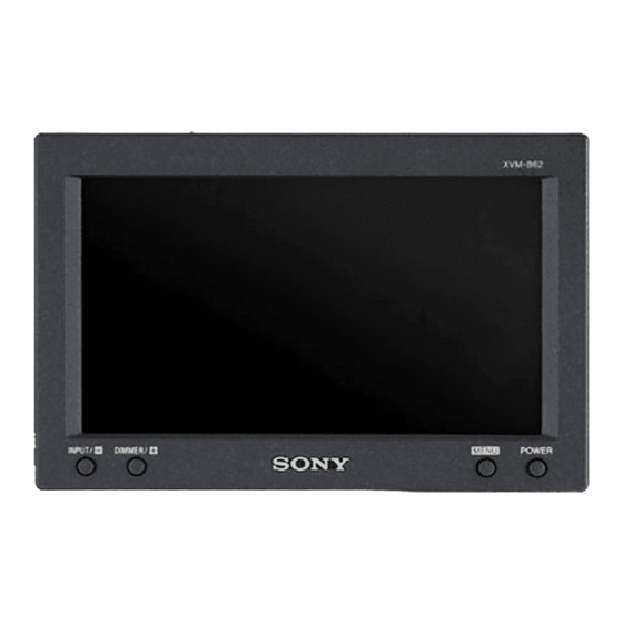
XVM-B62 SECTION 2 GENERAL This section is extracted from instruction manual. Location of controls Monitor 1 INPUT/ button Press to select the desired input source, VIDEO 1 or VIDEO 2. 2 DIMMER/ button Press to select the dimmer On/Off. 3 MENU button... -
Page 5: Connections
Monitor is optional. prevent them moving while your car • To attach the monitor using the supplied is in motion. collar, consult the store you purchased this unit or your nearest Sony dealer. -
Page 6: Connection Diagram
XVM-B62 Connection diagram Refer to the connection diagram for the proper connections. Mobile monitor XVM-B62 (6.2-inch wide color LCD Monitor) Video in cable (3 m) To the parking brake switch cord (see page 10) (To a metal surface of the car... -
Page 7: Disassembly
XVM-B62 SECTION 3 DISASSEMBLY Note: Follow the disassembly procedure in the numerical order given. 3-1. CASE (FRONT) SECTION 2 two screws (+B 2 × 5) 1 two screws 3 claw (+B 2 × 5) 4 claw 6 case (rear) section... -
Page 8: Test Mode
XVM-B62 SECTION 4 TEST MODE Setting Method: 1. Turn off power. 2. While holding the TEST switch (S408) down for more than 5 seconds, turn on power. Then, release the TEST switch (S408). 3. TEST MODE MENU is indicated. Terminating Method: Select the MENU No. -
Page 9: Electrical Adjustments
XVM-B62 SECTION 5 ELECTRICAL ADJUSTMENTS 5-1. EQUIPMENT USED 5-3. SETUP FOR ADJUSTMENT The following measuring equipment are used for these electrical The 10-step gray scale signal from the NTSC pattern generator is adjustments: used as an adjustment signal for V COM voltage/position adjustment •... -
Page 10: Dc-Dc Converter Adjustment
XVM-B62 5-4. DC-DC CONVERTER ADJUSTMENT 5-5. PLL ADJUSTMENT 5-4-1. Frequency Adjustment 5-5-1. Frequency Adjustment Adjustment Method: Adjustment Method: 1) Connect frequency counter between TP702 (+) and TP704 (–). 1) Connect digital voltmeter between TP807 (+) and TP808 (–). 2) Adjust RV702 so that the reading on the counter stands at the 2) Adjust RV802 so that the reading on the counter stands at the specified value. -
Page 11: Ntsc Subcarrier Check
XVM-B62 5-8. NTSC SUBCARRIER CHECK 5-11. VIDEO ADJUSTMENT 1. Subcarrier Check Conditions: TEST MODE (See 8 page) Checking Method: 10-step gray scale signal input 1) Press the [POWER] button and enter the NTSC mode using the NTSC mode [INPUT/+] and [DIMMER/--] buttons. -
Page 12: Rch Sub Bright Adjustment
XVM-B62 5-11-4. Rch Sub Bright Adjustment 5-11-7. B Sub Contrast Adjustment Adjustment Method: Adjustment Method: 1) Select R-Sub BRT from the FOR FACTORY MODE. 1) Select B-Sub CONT from the FOR FACTORY MODE. 2) Connect oscilloscope between TP722 (+) and TP723 (–). -
Page 13: Vco Free Run Adjustment
XVM-B62 5-11-10. VCO Free Run Adjustment 5-12. FLICKER AND WHITE BALANCE Adjustment Method: ADJUSTMENT 1) Select VCO Free Run from the FOR FACTOR MODE. Conditions: TEST MODE 2) Connect frequency counter between TP508 (+) and TP502 (–). NTSC all white 30% and all white 50% signal inputs... - Page 14 XVM-B62 Adjustment Location: – MAIN BOARD – (SIDE A) TP708 TP709 TP704 TP710 IC701 TP705 TP723 TP606 TP707 TP808 TP807 TP702 TP706 TP654 IC652 TP722 TP725 TP721 TP720 TP413 TP564 TP412 TP503 TP411 TP414 TP502 TP605 TP415 TP410 TP565 IC903...
-
Page 15: Diagrams
XVM-B62 SECTION 6 DIAGRAMS 6-1. BLOCK DIAGRAM — VIDEO SECTION — V SYNC SELECT IC503 H PULSE DELAY SHAPE Q506,507 Q514 VD PULSE C SYNC SHAPE BUFFER Q505,512,513 IC804 RGB DECODER, VIDEO PROCESSOR IC501 (Page 16) HSYNCLOCK VD IN HDOUT... -
Page 16: Block Diagram -Display Section
XVM-B62 6-2. BLOCK DIAGRAM — DISPLAY SECTION — (Page 15) GREEN DOT CLOCK IC802 BLUE D803 RV802 CPH1 OCPH1 STHL OSTH1 IVIY STHH (Page 15) ICSY OOEH STHR IOHSY OSTH2 LCD1 LIQUID CRYSTAL OCPV DISPLAY INNP DISPLAY STV1 PANEL CONTROL... - Page 17 XVM-B62 • Waveforms (MAIN Board) THIS NOTE IS COMMON FOR PRINTED WIRING BOARDS AND SCHEMATIC DIAGRAMS. (In addition to this, the necessary note is IC401 r; (X2) IC501 wk (VCOMOUT) IC501 yd (VXO-NTSC) IC801 r; (OSTV2) printed in each block.) for schematic diagram: •...
-
Page 18: Printed Wiring Board -Main Section
XVM-B62 6-3. PRINTED WIRING BOARD — MAIN SECTION — : Uses unleaded solder. L801 TP704 R844 TP708 D707 D706 TP709 R708 R865 Q801 TP705 L703 L803 TP710 C812 IC701 R850 TP723 R715 TP808 TP606 C714 Q656 C808 TP707 R843 R867... - Page 19 XVM-B62 LCD1 LIQUID CRYSTAL DISPLAY PANEL C718 L709 L707 D705 C713 L702 C725 Q702 D801 L706 C724 L708 D704 C710 L710 R856 C726 C717 R719 C727 L711 R823 BACK D703 R406 T701 C716 L705 D403 LIGHT C730 R824 Q415 Q416...
-
Page 20: Schematic Diagram -Main Section (1/2)
XVM-B62 6-4. SCHEMATIC DIAGRAM — MAIN SECTION (1/2) — • Refer to page 17 for Waveforms and page 23 for IC Block Diagrams and page 25 for IC Pin Description. C561 C562 R551 R518 R519 R552 R517 TP561 R557 TP562... -
Page 21: Schematic Diagram -Main Section (2/2)
XVM-B62 6-5. SCHEMATIC DIAGRAM — MAIN SECTION (2/2) — • Refer to page 17 for Waveforms and page 24 for IC Block Diagram and page 27 for IC Pin Description. IC B/D L804 Q801 TP807 R828 R874 R876 C808 C815... -
Page 22: Printed Wiring Board -Connector Section
XVM-B62 6-6. PRINTED WIRING BOARD — CONNECTOR SECTION — 6-7. SCHEMATIC DIAGRAM — CONNECTOR SECTION — : Uses unleaded solder. CN1001 CN1002 TP1001 TP1003 CN1002 TP1002 TP1004 (Page 20) TP1005 TP1006 1-869-355- (11) MAIN BOARD CN404 (Page 19) CN1001 (11) -
Page 23: Ic Block Diagrams
XVM-B62 • IC Block Diagrams IC501 AN2546FH-AV (MAIN Board (1/2)) LOGIC LOGIC LOGIC PONRST LOGIC IICBUS SYNCSEPA 32 HDOUT COMDC 31 VDOUT PHASE SECAM BLACKADJ VSYNC 30 PWM HHKILL COMP DROP CLAMP 29 VCC3 VCOM 28 VCOMOUT CTRAPOUT VERT. COUNT... - Page 24 XVM-B62 IC751 µPD6467GR-546-E1 (MAIN Board (1/2)) 20 HSYNC SCLK 19 VSYNC DATA INPUT INSTRUCTION DECODER CONTROL SIGNALS SHIFT REGISTER DATA WRITE-IN CHARACTER SIZE H-ADDRESS DISPLAY ADDRESS VIDEO RAM REGISTER REGISTER CONTROL COUNTER REGISTER DATA BACK SELECT INTERRUPT V-SIZE H-POSITION H-ADDRESS...
- Page 25 XVM-B62 • IC Pin Description IC401 µPD780022AGK-C56-9ET-A (SYSTEM CONTROL) (MAIN BOARD (1/2)) Pin No. Pin Name Pin Description TEST Test mode setting input PW-ON Power ON control signal output — Not used (Open) — Not used (Open) — Not used (Open) —...
- Page 26 XVM-B62 Pin No. Pin Name Pin Description — Not used (Open) P-ONSW — Not used (Pull down) — Not used (Open) — Not used (Open) — Not used (Open) — Not used (Open) — Not used (Open) TFT_ON LCD blacklight ON/OFF signal output...
- Page 27 XVM-B62 IC801 PVI1004D (DISPLAY CONTROLLER) (MAIN BOARD (2/2)) Pin No. Pin Name Pin Description IVSYNC — Not used (Open) IVIY Vertical sync signal input IFRST Reset signal input ICSY Horizontal sync signal input ICOMPS Composite/separate sync mode select input (Fixed at “L”) ICLKC —...
- Page 28 XVM-B62 Pin No. Pin Name Pin Description OCPH2 — Not used (Open) OCPH3 — Not used (Open) OSTH1 LCD driver start pulse output OSTH2 LCD driver start pulse output OQ4H — Not used (Open) LVDD — Power supply (+3.3V) OOEH...
-
Page 29: Exploded Views
XVM-B62 SECTION 7 EXPLODED VIEWS NOTE: • The mechanical parts with no reference • Color Indication of Appearance Parts The components identified by mark 0 or dotted line with mark. number in the exploded views are not supplied. Example : 0 are critical for safety. -
Page 30: Front Section
XVM-B62 7-2. FRONT SECTION not supplied not supplied not supplied LCD1 not supplied Ref. No. Part No. Description Remark Ref. No. Part No. Description Remark 2-662-642-01 BUTTON (POWER) 3-318-203-01 SCREW (B 1.7X6), TAPPING X-2109-199-1 CASE (FRONT) (SV) ASSY LCD1 1-802-054-11 DISPLAY PANEL, LIQUID CRYSTAL... -
Page 31: Electrical Parts List
XVM-B62 SECTION 8 CONNECTOR MAIN ELECTRICAL PARTS LIST NOTE: • Due to standardization, replacements in • Items marked “*” are not stocked since The components identified by mark 0 or dotted line with mark. the parts list may be different from the they are seldom required for routine service. - Page 32 XVM-B62 MAIN Ref. No. Part No. Description Remark Ref. No. Part No. Description Remark C603 1-162-970-11 CERAMIC CHIP 0.01uF C815 1-107-826-11 CERAMIC CHIP 0.1uF C604 1-162-970-11 CERAMIC CHIP 0.01uF C816 1-164-739-11 CERAMIC CHIP 560PF C605 1-107-826-11 CERAMIC CHIP 0.1uF C817 1-107-826-11 CERAMIC CHIP 0.1uF...
- Page 33 XVM-B62 MAIN Ref. No. Part No. Description Remark Ref. No. Part No. Description Remark < FILTER > Q502 8-729-905-35 TRANSISTOR 2SC4081-R Q503 8-729-905-35 TRANSISTOR 2SC4081-R FL801 1-239-896-12 FILTER, EMI (SMD) Q505 8-729-905-35 TRANSISTOR 2SC4081-R Q506 8-729-905-35 TRANSISTOR 2SC4081-R < IC >...
- Page 34 XVM-B62 MAIN Ref. No. Part No. Description Remark Ref. No. Part No. Description Remark R439 1-216-864-11 SHORT CHIP R537 1-216-829-11 METAL CHIP 4.7K 1/10W R441 1-216-809-11 METAL CHIP 1/10W R538 1-216-833-11 METAL CHIP 1/10W R442 1-216-809-11 METAL CHIP 1/10W R539...
- Page 35 XVM-B62 MAIN Ref. No. Part No. Description Remark Ref. No. Part No. Description Remark R708 1-216-839-11 METAL CHIP 1/10W R901 1-216-843-11 METAL CHIP 1/10W R709 1-218-885-11 METAL CHIP 0.5% 1/10W R902 1-218-892-11 METAL CHIP 0.5% 1/10W R710 1-218-885-11 METAL CHIP 0.5%...
-
Page 36: Revision History
XVM-B62 REVISION HISTORY Clicking the version allows you to jump to the revised page. Also, clicking the version at the upper on the revised page allows you to jump to the next revised page. Ver. Date Description of Revision 2006.02...
Need help?
Do you have a question about the XVM-B62 and is the answer not in the manual?
Questions and answers