Table of Contents
Advertisement
Mar. 2011
Table of Contents
Cautionary Notes ..............................................................2
Specifications .....................................................................2
Location of Controls .........................................................4
Location of Controls Parts List........................................5
Exploded View (1).............................................................6
Exploded View (1) Parts List ...........................................6
Exploded View (2).............................................................8
Exploded View (2) Parts List ...........................................9
Disassembly Procedure ....................................................9
Wiring Diagram/Block Diagram..................................10
Parts List ...........................................................................12
Verifying the Version......................................................14
Copyright © 2011 Roland Corporation
All rights reserved. No part of this publication may be reproduced in any form without the written permission
of Roland Corporation.
Data Backup and Restore Operations ..........................14
Performing a Factory Reset............................................14
Formatting the microSD Card .......................................14
Updating the System ......................................................14
Test Mode .........................................................................15
Circuit Board (Jack, DC Jack Board) .............................20
Circuit Diagram (Jack Board: Digital) ..........................22
Circuit Diagram (Jack Board: Analog) .........................24
Circuit Board (Panel, XLR Board) .................................28
Circuit Diagram (Panel, XLR Board) ............................30
17058737E0
SERVICE NOTES
Issued by RJA
RC-30
CC-KWS
Advertisement
Table of Contents

Related Manuals for Boss RC-30


Summary of Contents for Boss RC-30
-
Page 1: Table Of Contents
Mar. 2011 RC-30 SERVICE NOTES Issued by RJA Table of Contents Cautionary Notes ..............2 Data Backup and Restore Operations ......14 Specifications ..............2 Performing a Factory Reset..........14 Location of Controls ............4 Formatting the microSD Card ........14 Location of Controls Parts List........5 Updating the System ............14... -
Page 2: Cautionary Notes
Mar. 2011 RC-30 Cautionary Notes Specifications Before beginning the procedure, please read RC-30: Loop Station through this document. The matters described may differ according to the model. Nominal Input Level MIC IN: -40 dBu (variable) INST IN: -20 dBu Back Up User Data! - Page 3 Mar. 2011 RC-30 Indicators Options (sold separately) POWER indicator AC Adaptor (PSA series) REC, PLAY (DUB) indicator Foot Switch (FS-5U, FS-6) PEAK indicator TRACK 1 STATUS indicator TRACK 2 STATUS indicator BEND DOWN indicator * 0 dBu = 0.775 Vrms STEP PHASER indicator * Printed matters will not be supplied after the end of the production.
-
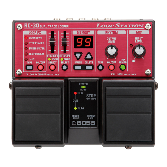
Page 4: Location Of Controls
Mar. 2011 RC-30 Location of Controls fig.panel.eps... -
Page 5: Location Of Controls Parts List
Mar. 2011 RC-30 Location of Controls Parts List Part Code Part Name Description Q’ty 5100018735 CASE 5100018736 PANEL 5100018740 7SEG COVER 5100021083 SA39-11SURKWA-3.3 5100018737 LED PANEL 15029281 LED (RED) GL-3PR8 03349989 LED (GREEN) L-34GDSL-FPB F2477102R0 S-KNOB 5100018742 POT DUST COVER... -
Page 6: Exploded View (1)
Mar. 2011 RC-30 Exploded View (1) fig.bunkaizu-bottom.eps Exploded View (1) Parts List Part Code Part Name Description Q’ty 5100008053 BOTTOM COVER (75D422E0R0) 5100008052 BOTTOM FOOT (G2357118R0) 5100008056 BATTERY COVER (G2017621R0) 5100008058 TWIN BATTERY CASE V6 (G2017620R0) 5100008059 BATTERY TERMINAL (+) - Page 7 Mar. 2011 RC-30...
-
Page 8: Exploded View (2)
Mar. 2011 RC-30 Exploded View (2) fig.bunkaizu-e.eps Attach the wiring so that it is on the outer side. LEFT SIDE RIGHT SIDE... -
Page 9: Exploded View (2) Parts List
Mar. 2011 RC-30 Exploded View (2) Parts List Parts Part Code Part Name Description Q’ty 5100018735 CASE 5100018736 PANEL 5100018737 LED PANEL 5100018738 REAR PANEL 5100018739 ESCUTCHEON 5100018740 7SEG COVER 5100018741 RUBBER SW 5100018742 POT DUST COVER 03344934 R-KNOB (G2477122/75D522N0R0) -
Page 10: Wiring Diagram/Block Diagram
Mar. 2011 RC-30 Wiring Diagram/Block Diagram fig.BLOCK.eps@L Part Code Part Name Description Q’ty 5100019608 WIRING W2 (MAIN) 5100019608 WIRING W2 (MAIN) 5100018920 WIRING W1 (MIC) 5100010465 WIRING 3P L=53X6X6MM P=2.0... - Page 11 Mar. 2011 RC-30 fig.BLOCK.eps@R...
-
Page 12: Parts List
Mar. 2011 RC-30 Parts List fig.-part1-e.eps Due to one or more of the following reasons, Safety Precautions: parts with parts code ******** cannot be supplied as service parts. The parts marked have safety-related characteristics. Use only listed parts for replacement. - Page 13 Mar. 2011 RC-30 SCREWS 5100008243 SCREW 2.6X5 (H5019430R0) BINDING HEAD TAPTITE P FEZC 40012489 SCREW 2.6X10 BINDING TAPTITE P FE BZC 5100008242 SCREW 3X6 (H5019110R0) PAN TAPPING B1 ZC 5100008245 SCREW 3X8 (H5019115R0) PAN TAPPING B1 BZC 5100008241 BTN M4D3 BOLT BZC...
-
Page 14: Verifying The Version
Terminate the USB connection correctly, according to the proper operation procedure for the computer. Making Written Notes Detach the USB cable from the RC-30. The data shown below cannot be backed up or restored. If any values differ The message U.P appears on the 7-segment LED display. -
Page 15: Test Mode
Mar. 2011 RC-30 Test Mode Quitting the Test Mode Disconnect the plug from the OUTPUT L/MONO jack. Items Required Selecting or Skipping Test Items • Noise meters x 2 • Oscilloscope x 1 Selecting and executing a specific test item is not possible. Skipping test items •... - Page 16 Mar. 2011 RC-30 3. LED & SW Check 5. CTL PEDAL Test Verify that all LEDs and the 7-segment LED display are dark. Verify that F1 is shown on the 7-segment LED display. Press each button in the sequence shown in the table below, and verify Depress the FS-5U connected to the FOOT SW jack (tip end).
- Page 17 Mar. 2011 RC-30 Disconnect the plug from the OUTPUT R jack and verify that the Make the following settings on the DI-1. waveform on channel 1 changes. ATT: 0 dB, Ø: NOR, GND: NOR fig.audio-3.eps Make the following settings on the oscilloscope.
- Page 18 Mar. 2011 RC-30 14. Disconnect the plugs from the INST IN L and R jacks. 13. Battery Detection Circuit Test 15. Input the following signal to AUX IN. Connect the stabilized power supply (5.8 V) to the DC jack. 200-Hz rectangular wave at 250 mVp-p (L and R) * Alternatively, connect a battery set at 5.8 V to the battery snap.
- Page 19 Mar. 2011 RC-30...
-
Page 20: Circuit Board (Jack, Dc Jack Board)
Mar. 2011 RC-30 Circuit Board (Jack, DC Jack Board) fig.b-JACK-1.eps... - Page 21 Mar. 2011 RC-30 fig.b-JACK-2.eps...
-
Page 22: Circuit Diagram (Jack Board: Digital)
Mar. 2011 RC-30 Circuit Diagram (Jack Board: Digital) fig.d-JACK-Digital.eps@L D+3.1 MA(0:1 D+3.1 XSF-WP TO JTAG BOARD XSD-PWR MA(15) AA15 MA(14) XREST RA18 D+1.2 MA(11) D+3.1 AA14 MA(10) AA19 14FMN-BMTTN-A-TF (LF)(SN) MA(9) DGND MA(8) UnPop AA18 MA(7) MA(6) TRI-STATE 0.1uF MA(5) - Page 23 Mar. 2011 RC-30 fig.d-JACK-Digital.eps@R MD(0:15) TP37 TC7WU04FU(TE12L.F) R104 TC7WU04FU(TE12L.F) D+3.1 TC7WU04FU(TE12L.F) DGND R103 D+3.1 D+1.2 E3SB16.9344F12D33 15pF 15pF 0.1uF TC7WU04FU(TE12L.F) 0.1uF DGND DGND D+1.2 DGND UnPop XBYPASS UnPop RA19 XPHANTOM-SW 22pF XPEDAL-R-SW 2.7k 22pF 0.1uF XPEDAL-L-SW 22pF 22pF DGND SD CARD...
-
Page 24: Circuit Diagram (Jack Board: Analog)
Mar. 2011 RC-30 Circuit Diagram (Jack Board: Analog) fig.d-JACK-Analog.eps@L TP149 TP52 TP63 TP64 R170 C170 AVCC D ( 0.5% ) 10uF 16V 1SS362FV(TPL3) MIC-OUT TP39 TP40 INST IN L(MONO) C107 47pF AGND TP50 1800pF D ( 0.5% ) TP41 2SK880-GR(TE85R.F) - Page 25 Mar. 2011 RC-30 fig.d-JACK-Analog.eps@R AVCC TP95 TP82 TP88 TP97 UnPop TP96 C127 10uF 16V D ( 0.5% ) UnPop R23 UnPop R101 C141 10uF 16V C186 XBYPASS UnPop D ( 0.5% ) DTC114TUAT106 UnPop AGND A+3.3 UnPop TP98 DGND TP69...
-
Page 26: Circuit Diagram (Jack Board: Power, Dc Jack Board)26
Mar. 2011 RC-30 Circuit Diagram (Jack Board: Power, DC Jack Board) fig.d-JACK-Power.eps@L TP104 TP111 R190 MINISMDC075F-2 53014-0210 BATT+ 53014-0210 BATT- TP103 TP106 TP105 TP122 SS14 MCH6306-TL-E WIRING RIBBON 3P/AWG26/P2.0 KM02009BB D3 6 UnPop TP113 D2 5 C146 D1 2 R212... - Page 27 Mar. 2011 RC-30 fig.d-JACK-Power.eps@R TP123 AVCC PVCC 100uF 220uF AGND PVCC 68uH CDRH4D28NP-680NC-R C100 0.1uF C101 47uF TP126 TP127 DGND DGND TP132 TP130 +48V TP128 TP125 R120 R141 UnPop C117 R142 TP124 MONIN 4.7uF FSET VOUT2 _SHDN VOUT1 DTC114TUAT106 R121...
-
Page 28: Circuit Board (Panel, Xlr Board)
Mar. 2011 RC-30 Circuit Board (Panel, XLR Board) fig.b-PANEL-1.eps... - Page 29 Mar. 2011 RC-30 fig.b-PANEL-2.eps...
-
Page 30: Circuit Diagram (Panel, Xlr Board)
Mar. 2011 RC-30 Circuit Diagram (Panel, XLR Board) fig.d-PANEL-XLR.eps@L XLR BOARD JY-5033A*030 SV69010F-0202-6V-NP-001 SV69010F-0202-6V-NP-001 SV69010F-0202-6V-NP-001 SV69010F-0202-6V-NP-001 B2011H02-5P A2001WR2-5P Right Angle TP86 TP89 TP90 TP87 TP88 Board In Wiring Straight Angle TRACK1 RHYTHM TYPE DELETE LOOP FX ON/OFF WRITE LOOP FX SEL... - Page 31 Mar. 2011 RC-30 fig.d-PANEL-XLR.eps@R +48V TP95 0.01uF MIC INPUT LEVEL VOL TP96 TP106 TP137 TP107 100k AVCC 100k 10uF 2SA1587-GR(TE85L.F) TP104 TP103 PHANTOM-ON TP164 DTC114EUAT106(PB FREE) 4.7k RD901F-40-125F-A50K-00DQ8 D ( 0.5% ) 50kA AVCC 47pF 0.018uF D ( 0.5% )
Need help?
Do you have a question about the RC-30 and is the answer not in the manual?
Questions and answers